background image

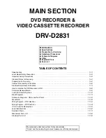
SERVICE MANUAL

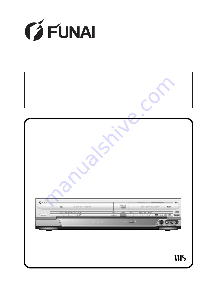
DVD RECORDER & 

VIDEO CASSETTE RECORDER

DRV-D2831

Main Section

I

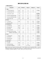
 Specifications

I

 Preparation for Servicing

I

 Adjustment Procedures

I

 Schematic Diagrams

I

 CBA’s

I

 Exploded views

I

 Parts List

When servicing the deck 
mechanism, refer to MK14 Deck 
Mechanism Section.

Deck Mechanism Part No.: 
N25E0FL

PA L

Summary of Contents for DRV-A2635

Page 1: ...V D2831 Main Section I Specifications I Preparation for Servicing I Adjustment Procedures I Schematic Diagrams I CBA s I Exploded views I Parts List When servicing the deck mechanism refer to MK14 Dec...

Page 2: ...unction Indicator Symbols 1 10 1 Block Diagrams 1 11 1 Schematic Diagrams CBA s and Test Points 1 12 1 Waveforms 1 13 1 Wiring Diagram VCR Section 1 14 1 Wiring Diagram DVD Section 1 14 2 IC Pin Funct...

Page 3: ...de W O Burst 1 4 Video Color S N AM R P dB 37 41 SP Mode 1 5 Video Color S N PM R P dB 30 36 SP Mode 1 6 Resolution PB Line 230 245 SP Mode 2 Servo 2 1 Jitter Low sec 0 07 0 12 SP Mode 2 2 Wow Flutter...

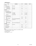
Page 4: ...load Vp p 1 0 C Chrominance 75 load Vp p 0 3 2 AUDIO 2 1 Output Level Vrms 2 0 2 2 Frequency Response DVD VIDEO LPCM fs 96 kHz Hz 20 44 k fs 48 kHz Hz 20 20 k Audio CD fs 44 1 kHz Hz 20 20 k 2 3 Signa...

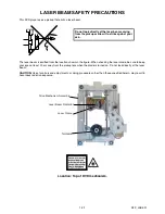
Page 5: ...m away from the pickup lens when the diode is turned on Do not look directly at the laser beam CAUTION Use of controls and adjustments or doing procedures other than those specified herein may result...

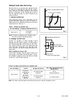
Page 6: ...especially 1 Wires covered with PVC tubing 2 Double insulated wires 3 High voltage leads D Use specified insulating materials for hazardous live parts Note especially 1 Insulation tape 2 PVC tubing 3...

Page 7: ...age Current Test Confirm the specified or lower leakage current between B earth ground power cord plug prongs and externally exposed accessible parts RF termi nals antenna terminals video and audio in...

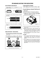
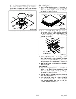
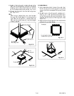
Page 8: ...achine then apply hot air to the Flat Pack IC about 5 to 6 seconds Fig S 1 1 2 Remove the flat pack IC with tweezers while apply ing the hot air 3 Bottom of the flat pack IC is fixed with glue to the...

Page 9: ...removing entire flat pack IC first apply soldering iron to center of the flat pack IC and heat up Then remove glue will be melted Fig S 1 6 4 Release the flat pack IC from the CBA using twee zers Fig...

Page 10: ...Installation 1 Using desoldering braid remove the solder from the foil of each pin of the flat pack IC on the CBA so you can install a replacement flat pack IC more easily 2 The I mark on the flat pac...

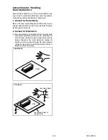
Page 11: ...ed to remove any static electricity that may be charged on the body 2 Ground for Workbench 1 Be sure to place a conductive sheet or copper plate with proper grounding 1M on the workbench or other surf...

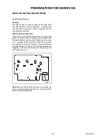
Page 12: ...nto the Deck Mechanism Assembly and press the PLAY button The tape will be loaded into the Deck Mechanism Assembly Make sure the power is on connect TP501 S INH to GND This will stop the function of T...

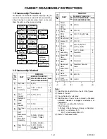
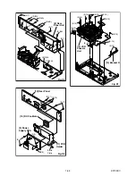
Page 13: ...ion Sheet D2 5 Jack Bracket D3 2 S 4 6 Front Jack CBA D3 Jack Earth Plate 7 DVD Mechanism DVD Main CBA Assembly D4 2 S 5A 2 S 5B CN501 CN601 8 Rear Panel Unit D5 2 S 6A 2 S 6B 3 S 7 S 8A S 8B CN1503 C...

Page 14: ...installing the Deck Assembly be sure to place the pin of LD SW on Main CBA as shown in Fig D8 Then install the Deck Assembly while aligning the hole of Cam Gear with the pin of LD SW the shaft of Cam...

Page 15: ...8B CN1503 CN1504 S 8A 8 Rear Panel Unit Fig D6 S 11 S 11 S 9 S 9 S 9 S 10 12 Rear Panel 9 Power Supply CBA 11 PCB Holder 10 DC Fan Motor Earth Plate Fig D7 S 13 S 13 S 13 S 14 S 15 S 16 S 14 S 14 S 1...

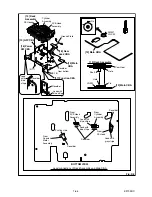
Page 16: ...OM VIEW Lead connections of Deck Assembly and Main CBA Desolder From Capstan Motor Assembly Printing side Desolder From Cylinder Assembly From ACE Head Assembly Lead with blue stripe Lead with blue st...

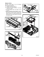
Page 17: ...as shown below When rotating the gear be careful not to damage the gear 1 Remove the Top Cover 2 Rotate the gear in the direction of the arrow manually as shown below Fig D9 20 Deck Pedestal 21 Front...

Page 18: ...Assembly Then remove the DVD Mechanism Unit 2 Remove two screws and remove the Insulating Plate 3 Release two Locking Tabs and lift up one side of the Clamper Assembly 4 Release the other side of two...

Page 19: ...trace with 10 1 probe V Range 0 001 50V Div F Range DC AC 20MHz 2 Alignment Tape FL6A Head Switching Position Adjustment Purpose To determine the Head Switching position during playback Symptom of Mis...

Page 20: ...ing When the initializing is completed the DVD recorder exits the Version display mode and turns off the power automatically To move into the Normal mode from the Version display mode press RETURN but...

Page 21: ...n XX is displayed on the VFD The appearance shown in 1 of Fig d is described as follows Fig a Version Up Mode Screen Firmware Version differs depending on the models and this indication is one example...

Page 22: ...At this time no button is available 6 Press STANDBY ON button to turn the power off Then press it again Fig f Completed Program Mode Screen Firmware Version differs depending on the models and this i...

Page 23: ...E When reel or capstan mechanism is not functioning correctly A R is displayed on a TV screen Refer to Fig 1 When tape loading mechanism is not func tioning correctly A T is displayed on a TV screen R...

Page 24: ...e 14 Cannot write the data after recovering SMALL VMGI 15 Cannot write the data after DVD R Reverse Track 16 An error occurs in Finalize Close 17 An error occurs in Rec Stop Close 18 An error occurs i...

Page 25: ...ot a space to a record field of control information 10 You cannot record on the disc as Power Calibration Area is full Insert a new disc 35 PCA Full in REC start 4 This disc is already finalized Relea...

Page 26: ...BA 1 1 OPEN CLOSE SW 2 2 DUBBING SW CN510 CN681 FUNCTION CBA 86 19 83 DRV DATA DVD LED VCR LED 1G 7G a i 68 DRV CLK 70 DRV STB DRV DIN DRV CLK DRV STB 69 7 3 2 20 28 42 36 8 9 IIC BUS SCL D V SYNC D R...

Page 27: ...S BCK DATA LRCK SYSCLK E20 H18 K18 H19 G19 W17 T20 N19 M19 V4 W4 V3 U20 H20 G20 F20 P19 VIDEO Y I P VIDEO C VIDEO Cb Pb VIDEO Cr Pr VIDEO Y CVBS VIDEO C IC202 FLASH MEMORY D A D A D A D A AUDIO I F VI...

Page 28: ...1 HEAD VIDEO L 2 HEAD VIDEO R 2 HEAD VIDEO L 2 VIDEO COM VIDEO R 2 4 5 6 IC301 VIDEO SIGNAL PROCESS HEAD AMP IC501 OSD VCR VIDEO VCR VIDEO DUB VCR DVD DUBBING DVD VIDEO DUB PB EE VIDEO REC VIDEO SIGN...

Page 29: ...FFER LPF DVD MAIN CBA CN601 21 21 VIDEO Y CVBS 23 23 VIDEO C CN1502 CN1505 2 2 FRONT Y IN 1 1 FRONT C IN 4 4 FRONT VIDEO IN CN1201 Q1520 BUFFER Q1521 Q1541 BUFFER VIDEO SW1 VIDEO Y CVBS VIDEO C IC1518...

Page 30: ...W F 9 W F 5 W F 4 JK1502 JK2001 IC1515 VIDEO DRIVER 5 4dB AMP 2dB AMP LPF DRIVER 6 8dB AMP 6dB DRIVER 4dB AMP 2dB AMP LPF DRIVER 3 1 7 1 1 VIDEO Y I VIDEO Y I P VIDEO C VIDEO Cb Pb VIDEO Cr Pr VIDEO...

Page 31: ...TROL MUTE 11 6 PB ON SP LP ON P TUNER IN2 IN1 R ALC DET ALC IC301 AUDIO SIGNAL PROCESS 15 13 17 4 AUDIO PB REC CN504 3 A COM 1 AE H 2 AE H FE H AUDIO HEAD AUDIO ERASE HEAD ACE HEAD ASSEMBLY FE HEAD 2...

Page 32: ...3 13 4 5 11 1 12 14 MUTE ON DRIVE Q1540 MUTE ON 9 10 7 6 8 15 14 16 4 3 5 IC902 AUDIO A D CONVERTER AUDIO A D CONVERTER 10 11 12 1 2 15 SPDIF CN501 CN1501 CN601 CN1502 BCK DATA LRCK MD MC SCK 2 MS L C...

Page 33: ...DIO R DVD VCR DUBBING VCR AUDIO R DVD AUDIO L VCR AUDIO L LIM 80 N A PB Hi Fi H SW AUDIO MUTE 2 A MODE TO AUDIO BLOCK DIAGRAM TO AUDIO INPUT OUTPUT SELECT BLOCK DIAGRAM TO AUDIO INPUT OUTPUT SELECT BL...

Page 34: ...V 4 AL 2 4V 6 AL 4V 9 F1 8 2 4 6 9 8 F2 TO PIN 75 OF IC501 TO PIN 32 OF IC501 TO PIN 84 OF IC501 REG CONT TO PIN 42 OF IC501 IC1505 3 3V REG IC1504 2 5V REG JUNCTION CBA CN051A 1 3 5 10 1 3 5 8 8 10 1...

Page 35: ...stitute replacement parts that do not have the same safety characteristics as specified in the parts list may create shock fire or other hazards Notes 1 Do not use the part number shown on these drawi...

Page 36: ...acement parts which are listed with their part numbers in the parts list section of the service manual 4 Voltage indications for PLAY and REC modes on the schematics are as shown below 5 How to read c...

Page 37: ...1 12 3 E9709SCM1 Main 1 9 Schematic Diagram VCR Section...

Page 38: ...g c d e f g h h i a b a b a b a b a b FL601 MATRIX CHART REPEAT PM REC VCD VCR DVD R XP SP LP EP SLP P SCAN SEP W CD T C 5G 4G 3G 2G 1G 7G 6G a d g h h g c b e f REPEAT PM REC VCD VCR DVD R XP SP LP...

Page 39: ...1 12 5 E9709SCM3 Main 3 9 Schematic Diagram VCR Section...

Page 40: ...1 12 6 E9709SCM4 Main 4 9 Schematic Diagram VCR Section...

Page 41: ...1 12 7 E9709SCM5 Main 5 9 Schematic Diagram VCR Section...

Page 42: ...1 12 8 E9709SCM6 Main 6 9 Front Jack Schematic Diagram VCR Section...

Page 43: ...1 12 9 E9709SCM7 Main 7 9 Schematic Diagram VCR Section...

Page 44: ...1 12 10 E9709SCM8 Main 8 9 Schematic Diagram VCR Section...

Page 45: ...1 12 11 E9709SCM9 Main 9 9 Schematic Diagram VCR Section...

Page 46: ...check to see that all components in the power supply circuit are not defective before you connect the AC plug to the AC power supply Otherwise it may cause some components in the power supply circuit...

Page 47: ...1 12 13 E9709SCRJ Rear Jack Schematic Diagram VCR Section...

Page 48: ...1 12 14 E9709SCAFV AFV Schematic Diagram VCR Section...

Page 49: ...1 12 15 E9709SCD1 DVD Main 1 6 Schematic Diagram DVD Section...

Page 50: ...1 12 16 E9709SCD2 DVD Main 2 6 Schematic Diagram DVD Section...

Page 51: ...1 12 17 E9709SCD3 DVD Main 3 6 Schematic Diagram DVD Section...

Page 52: ...n 4 6 Schematic Diagram DVD Section NOTE 1 The order of pins shown in this diagram is different from that of actual IC601 2 IC601 is divided into six and shown as IC601 1 6 IC601 6 6 in this DVD Main...

Page 53: ...n 5 6 Schematic Diagram DVD Section NOTE 1 The order of pins shown in this diagram is different from that of actual IC601 2 IC601 is divided into six and shown as IC601 1 6 IC601 6 6 in this DVD Main...

Page 54: ...n 6 6 Schematic Diagram DVD Section NOTE 1 The order of pins shown in this diagram is different from that of actual IC601 2 IC601 is divided into six and shown as IC601 1 6 IC601 6 6 in this DVD Main...

Page 55: ...n CBA Top View Sensor CBA Top View BHF300F01011B BHF300F01011A TO SENSOR CBA END SENSOR SW P VR501 TP301 WF2 C PB CTL TP503 TP504 RF SW JK1 V OUT J236 WF3 S INH TP501 TO SENSOR CBA START SENSOR WF1 BE...

Page 56: ...1 12 22 PIN 9 OF CN1502 WF8 PIN 17 OF CN1502 WF6 PIN 7 OF CN1502 WF4 PIN 3 OF IC1502 WF5 PIN 5 OF CN1502 WF7 WF10 PIN 1 OF CN1501 WF9 PIN 6 OF IC1515 Main CBA Bottom View BE9700F01015A...

Page 57: ...1 12 23 Front Jack CBA Top View Front Jack CBA Bottom View Function CBA Top View Function CBA Bottom View Power SW CBA Top View Power SW CBA Bottom View BE9700F01015D BE9700F01015C BE9700F01015B...

Page 58: ...red CAUTION Fixed voltage or Auto voltage selectable power supply circuit is used in this unit If Main Fuse F1001 is blown check to see that all components in the power supply circuit are not defectiv...

Page 59: ...ired CAUTION Fixed voltage or Auto voltage selectable power supply circuit is used in this unit If Main Fuse F1001 is blown check to see that all components in the power supply circuit are not defecti...

Page 60: ...1 12 26 Rear Jack CBA Top View Rear Jack CBA Bottom View BH9700F01022C AFV CBA Top View AFV CBA Bottom View BE6800F01091 Junction CBA Top View Junction CBA Bottom View BE9700F01022B...

Page 61: ...SPDIF 1V 0 1 s WF10 Pin 1 of CN1501 WF6 Pin 7 of CN1502 VIDEO Y 0 2V 20 s WF7 Pin 9 of CN1502 VIDEO C 0 2V 20 s WF9 Pin 6 of IC1515 VIDEO CVBS 0 5V 20 s WF2 WF3 UPPER WF1 WF1 LOWER J236 TP504 UPPER L...

Page 62: ...O R 1 AL 16V 12V P ON 5V DECK C F R C FG C CONT GND LM FWD REV D CONT D PFG GND AL 12V 2 P ON 15V FE H GND FE H AE H AE H FE H A COM AUDIO PB REC CTL CTL F1 19 GND 17 AL 4V 16 GND 15 AL 2 4V 14 GND 13...

Page 63: ...13 VCC1 FOCUS ACTUATOR TRACKING ACTUATOR TILT ACTUATOR DVD CD LASER DIODE DRIVE PDIC FPDIC CD LD DVD LD TRAY OPEN SLED SENSOR SPINDLE MOTOR 1 2 3 AUDIO L OUT 17 GND 18 DVD AUDIO MUTE 19 AUDIO 5V 20 V...

Page 64: ...3 Video Input Select Signal 25 OUT REG CONT2 Power Regulator Control Signal 26 NU Not Used 27 OUT RGB THROUGH SCART 2 RGB Through Control Signal 28 OUT AUDIO MUTE 2 Audio Mute Control Signal 29 OUT DV...

Page 65: ...rol Signal 77 OUT D CONT Drum Motor Control Signal 78 OUT C F R Capstan Motor FWD REV Control Signal FWD L REV H 79 IN S REEL Supply Reel Rotation Signal 80 IN T REEL Take Up Reel Rotation Signal 81 O...

Page 66: ...Input 9 IN DRV STB Serial Interface Strobe 10 NU Not Used 11 NU Not Used 12 VSS GND 13 VDD Power Supply 14 NU Not Used 15 NU Not Used 16 NU Not Used 17 NU Not Used 18 NU Not Used 19 NU Not Used 20 OU...

Page 67: ...MID 32A22F PT204 6B 12 E C B1 E B2 C1 C2 FMG4A T148 RN1511 TE85R RN1511 TE85R F FA1F4M T1B KRC103S RTK KRC103S RTK P KTC3875S GR Y RTK P KTA1504 GR Y RTK KTA1504S GR Y RTK P KTC3879Y RTK KTC3879 Y RT...

Page 68: ...33 2B17 2L045 2L045 2B19 2B14 A2 2L033 2L033 2L033 C 2L111 2L110 2B9 2B9 2L022 2L021 2L054 2L052 JW001 2L017 2L017 2L017 2L017 2L017 2B1 2L014 2L061 2L015 E E D 2L015 2B11 A34 2B13 A34 C A1X A10 A14 J...

Page 69: ...1 17 2 E9709PEX Packing X1 A14 S1 S2 S2 S12 X6 S2 S2 S3 X9 X2 X3 X4 X20A X22F X22E X22G X22B X22A X22D X22C X20B X20C X20D X20E X20F X20G...

Page 70: ...3X8 BIND HEAD GBJP3080 2L044 P TIGHT SCREW 3X8 BIND or GBMP3080 SCREW P TIGHT M3X8 BIND HEAD GBJP3080 2L045 P TIGHT SCREW 3X8 BIND or GBMP3080 SCREW P TIGHT M3X8 BIND HEAD GBJP3080 2L052 SCREW P TIGHT...

Page 71: ...1JK30B223 CHIP CERAMIC CAP 1608 B K 0 022 F 25V CHD1EK30B223 C322 CHIP CERAMIC CAP 1608 F Z 0 1 F 50V or CHD1JZ30F104 CHIP CERAMIC CAP 1608 F Z 0 1 F 25V or CHD1EZ30F104 CHIP CERAMIC CAP FZ Z 0 1 F 50...

Page 72: ...CAP 1608 F Z 0 1 F 50V or CHD1JZ30F104 CHIP CERAMIC CAP 1608 F Z 0 1 F 25V or CHD1EZ30F104 Ref No Description Part No CHIP CERAMIC CAP FZ Z 0 1 F 50V CHD1JZ3FZ104 C502 CHIP CERAMIC CAP 1608 B K 0 022...

Page 73: ...1 F 50V or CHD1JZ30F104 CHIP CERAMIC CAP 1608 F Z 0 1 F 25V or CHD1EZ30F104 Ref No Description Part No CHIP CERAMIC CAP FZ Z 0 1 F 50V CHD1JZ3FZ104 C1540 CHIP CERAMIC CAP 1608 F Z 0 1 F 50V or CHD1JZ3...

Page 74: ...AMIC CAP B K 2200pF 50V CHD1JK30B222 C1640 CHIP CERAMIC CAP B K 2200pF 50V CHD1JK30B222 C1643 ELECTROLYTIC CAP 47 F 6 3V M or CE0KMASDL470 ELECTROLYTIC CAP 47 F 6 3V M CE0KMASTL470 C1648 CHIP CERAMIC...

Page 75: ...65 or NDTA00DZ11BS ZENER DIODE MTZJT 7711A QDTA00MTZJ11 D1542 ZENER DIODE DZ 11BSAT265 or NDTA00DZ11BS ZENER DIODE MTZJT 7711A QDTA00MTZJ11 Ref No Description Part No ICS IC301 IC Y C A LA71750EM MPB...

Page 76: ...3199P TRANSISTOR 2SC1815 Y TE2 F T or QQSY2SC1815F TRANSISTOR 2SC1815 GR TE2 F T or QQS12SC1815F TRANSISTOR 2SC2785 J or QQSJ02SC2785 TRANSISTOR 2SC2785 H or QQSH02SC2785 Ref No Description Part No TR...

Page 77: ...Y or NQSY0KTC3199 TRANSISTOR KTC3199 or NQS40KTC3199 TRANSISTOR 2SC1815 Y TPE2 or QQSY02SC1815 TRANSISTOR 2SC1815 GR TPE2 QQS102SC1815 Q1539 TRANSISTOR KTC3199 Y AT P or NQSYKTC3199P Ref No Descriptio...

Page 78: ...R5Z0562 R543 CARBON RES 1 4W J 1k RCX4JATZ0102 R544 CARBON RES 1 6W J 10k or RCX6JATZ0103 Ref No Description Part No CARBON RES 1 4W J 10k RCX4JATZ0103 R545 CARBON RES 1 6W J 10k or RCX6JATZ0103 CARBO...

Page 79: ...P RES 1 10W J 2 2k RRXAJR5Z0222 R1566 CHIP RES 1 10W J 6 8k RRXAJR5Z0682 Ref No Description Part No R1567 CHIP RES 1 10W J 6 8k RRXAJR5Z0682 R1568 CARBON RES 1 6W J 3 3k or RCX6JATZ0332 CARBON RES 1 4...

Page 80: ...0333 SWITCHES SW506 LEAF SWITCH MXS01830MVP0 SSC0101MCE03 Ref No Description Part No SW507 ROTARY MODE SWITCH SSS 53MD SSR0106KB003 SW521 TACT SWITCH KSM0614B or SST0101HH013 TACT SWITCH SKQSAF001A or...

Page 81: ...T204 6B 12 or NPWZT2046B12 PHOTO TRANSISTOR MID 32A22F NPWZ1D32A22F Ref No Description Part No PSV CBA Consists of the following 1VSA11670 POWER SUPPLY CBA PSV A JUNCTION CBA PSV B REAR JACK CBA PSV C...

Page 82: ...B0810T 470K LLBD00PU6007 L1001 BEAD CORE ASSEMBLY E9700ED 1VSA11692 Ref No Description Part No L1002 BEAD CORE ASSEMBLY E9700ED 1VSA11692 L1003 LINE FILTER 56MH TLF14CB5630R2 or LLBG00ZTU022 LINE FILT...

Page 83: ...65 or NDTA00DZ11BS Ref No Description Part No ZENER DIODE MTZJT 7711A QDTA00MTZJ11 D2004 ZENER DIODE DZ 11BSAT265 or NDTA00DZ11BS ZENER DIODE MTZJT 7711A QDTA00MTZJ11 D2005 ZENER DIODE DZ 11BSAT265 or...

Page 84: ...E1CMASSL100 C16 ELECTROLYTIC CAP 10 F 16V M H7 CE1CMASSL100 C17 CHIP CERAMIC CAP 1608 F Z 0 1 F 50V or CHD1JZ30F104 CHIP CERAMIC CAP 1608 F Z 0 1 F 25V or CHD1EZ30F104 CHIP CERAMIC CAP FZ Z 0 1 F 50V...

Page 85: ...DRV D2831 E9709ED 2005 10 27...

Reviews: