background image

Exar

 Corporation 48720 Kato Road, Fremont CA, 94538 

 (510) 668-7000 

 FAX (510) 668-7017 

 www.exar.com 

xr

PRELIMINARY

XRT86VL38

OCTAL T1/E1/J1 FRAMER/LIU COMBO

MARCH 2005

REV. P1.0.6 

GENERAL DESCRIPTION

The XRT86VL38 is an eight-channel 1.544 Mbit/s or 
2.048 Mbit/s DS1/E1/J1 framer and LIU integrated 

solution featuring R

3

 technology (Relayless, 

Reconfigurable, Redundancy).  The physical 
interface is optimized with internal impedance, and 
with the patented pad structure, the XRT86VL38 
provides protection from power failures and hot 
swapping.

The XRT86VL38 contains an integrated DS1/E1/J1 
framer and LIU which provide DS1/E1/J1 framing and 
error accumulation in accordance with ANSI/ITU_T 
specifications. Each framer has its own framing 
synchronizer and transmit-receive slip buffers.  The 
slip buffers can be independently enabled or disabled 
as required and can be configured to frame to the 
common DS1/E1/J1 signal formats.

Each Framer block contains its own Transmit and 
Receive T1/E1/J1 Framing function. There are 3 
Transmit HDLC controllers per channel which 
encapsulate contents of the Transmit HDLC buffers 
into LAPD Message frames. There are 3 Receive 
HDLC controllers per channel which extract the 

payload content of Receive LAPD Message frames 
from the incoming T1/E1/J1 data stream and write the 
contents into the Receive HDLC buffers. Each framer 
also contains a Transmit and Overhead Data Input 
port, which permits Data Link Terminal Equipment 
direct access to the outbound T1/E1/J1 frames. 
Likewise, a Receive Overhead output data port 
permits Data Link Terminal Equipment direct access 
to the Data Link bits of the inbound T1/E1/J1 frames.

The XRT86VL38 fully meets all of the latest T1/E1/J1 
specifications:   ANSI T1/E1.107-1988, ANSI T1/
E1.403-1995, ANSI T1/E1.231-1993, ANSI T1/
E1.408-1990, AT&T TR 62411 (12-90) TR54016, and 
ITU G-703, G.704, G706 and G.733, AT&T Pub. 
43801, and ETS 300 011, 300 233, JT G.703, JT 
G.704, JT G706, I.431. Extensive test and diagnostic 
functions include Loop-backs, Boundary scan, 
Pseudo Random bit sequence (PRBS) test pattern 
generation, Performance Monitor,


Bit Error Rate 

(BER) meter, forced error insertion, and LAPD 
unchannelized data payload processing according to 
ITU-T standard Q.921.

Applications and Features (next page)
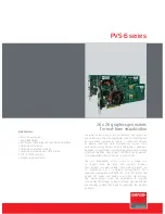
F

IGURE

 1.  XRT86VL38 8-

CHANNEL

 DS1 (T1/E1/J1) F

RAMER

/LIU C

OMBO

Performance

Monitor

PRBS

Generator &

Analyser

HDLC/LAPD

Controllers

LIU &

Loopback

Control

DMA

Interface

Signaling &

Alarms

JTAG

WR
ALE_AS
RD
RDY_DTACK

µ

P

Select

A[14:0]

D[7:0]

Microprocessor

Interface

4

3

Tx Serial

Clock

Rx Serial

Clock

8kHz sync

OSC

Back Plane

1.544-16.384 Mbit/s

Local PCM

Highway

ST-

BUS

2-Frame

Slip Buffer

Elastic Store

Tx Serial

Data In

Tx LIU

Interface

2-Frame

Slip Buffer

Elastic Store

Rx LIU

Interface

Rx Framer

Rx Serial
Data Out

RTIP

RRING

TTIP

TRING

External Data

Link Controller

Tx Overhead In

Rx Overhead Out

XRT86VL38

1 of 8-channels

Tx Framer

LLB

LB

System (Terminal) Side

Line Side

1:1 Turns Ratio

1:2 Turns Ratio

Memory

Intel/Motorola µP

Configuration, Control &

Status Monitor

RxLOS

TxON

INT

Summary of Contents for XRT86VL38

Page 1: ...permits Data Link Terminal Equipment direct access to the outbound T1 E1 J1 frames Likewise a Receive Overhead output data port permits Data Link Terminal Equipment direct access to the Data Link bits of the inbound T1 E1 J1 frames The XRT86VL38 fully meets all of the latest T1 E1 J1 specifications ANSI T1 E1 107 1988 ANSI T1 E1 403 1995 ANSI T1 E1 231 1993 ANSI T1 E1 408 1990 AT T TR 62411 12 90 ...

Page 2: ...44 2 048 4 096 and 8 192 Mbits Also supports 4 channel multiplexed 12 352 16 384 HMVIP H 100 Mbit s on the back plane bus Programmable output clocks for Fractional T1 E1 J1 Supports Channel Associated Signaling CAS Supports Common Channel Signalling CCS Supports ISDN Primary Rate Interface ISDN PRI signaling Extracts and inserts robbed bit signaling RBS 3 Integrated HDLC controllers per channel fo...

Page 3: ...F LOF LOS errors and COFA conditions Loopbacks Local LLB and Line remote LB Facilitates Inverse Multiplexing for ATM Performance monitor with one second polling Boundary scan IEEE 1149 1 JTAG test port Accepts external 8kHz Sync reference 1 8V Inner Core Voltage 3 3V I O operation with 5V tolerant inputs 420 pin TBGA package or 484 pin STBGA package with 40 C to 85 C operation ORDERING INFORMATION...

Page 4: ... O O O O O O O O O O O O E O O O O O O O O O O F O O O O O O O O O O G O O O O O O O O O O H O O O O O O O O O O J O O O O O O O O O O K O O O O O O O O O O L O O O O O O O O O O M O O O O O O O O O O N O O O O O O O O O O P O O O O O O O O O O R O O O O O O O O O O T O O O O O O O O O O U O O O O O O O O O O V O O O O O O O O O O W O O O O O O O O O O Y O O O O O O O O O O AA O O O O O O O O O O ...

Page 5: ... O O O O O O O O G O O O O O O O O O O O O O O O O O O O O O O H O O O O O O O O O O O O O O O O O O O O O O J O O O O O O O O O O O O O O O O O O O O O O K O O O O O O O O O O O O O O O O O O O O O O L O O O O O O O O O O O O O O O O O O O O O O M O O O O O O O O O O O O O O O O O O O O O O N O O O O O O O O O O O O O O O O O O O O O O P O O O O O O O O O O O O O O O O O O O O O O R O O O O O O O...

Page 6: ...NTERFACE WITH 1 1 AND 1 1 REDUNDANCY 309 4 3 POWER FAILURE PROTECTION 310 4 4 OVERVOLTAGE AND OVERCURRENT PROTECTION 310 4 5 NON INTRUSIVE MONITORING 310 4 6 T1 E1 SERIAL PCM INTERFACE 311 4 7 T1 E1 FRACTIONAL INTERFACE 312 4 8 T1 E1 TIME SLOT SUBSTITUTION AND CONTROL 313 4 9 ROBBED BIT SIGNALING CAS SIGNALING 314 4 10 OVERHEAD INTERFACE 315 4 11 FRAMER BYPASS MODE 317 4 12 HIGH SPEED NON MULTIPLE...

Page 7: ...E OVERHEAD OUTPUT INTERFACE MODULE AS DESTINATION OF THE SIGNALING FRAMING FS BITS IN N OR SLC 96 FRAMING FORMAT MODE 338 6 2 4 CONFIGURE THE DS1 RECEIVE OVERHEAD OUTPUT INTERFACE MODULE AS DESTINATION OF THE REMOTE SIGNALING R BITS IN T1DM FRAMING FORMAT MODE 339 6 3 E1 OVERHEAD INTERFACE BLOCK 340 6 4 E1 TRANSMIT OVERHEAD INPUT INTERFACE BLOCK 340 6 4 1 DESCRIPTION OF THE E1 TRANSMIT OVERHEAD IN...

Page 8: ...1 2 RED ALARM 388 11 3 YELLOW ALARM 389 11 4 BIPOLAR VIOLATION 391 11 5 E1 BRIEF DISCUSSION OF ALARMS AND ERROR CONDITIONS 393 11 5 1 HOW TO CONFIGURE THE FRAMER TO TRANSMIT AIS 399 11 5 2 HOW TO CONFIGURE THE FRAMER TO GENERATE RED ALARM 400 11 5 3 HOW TO CONFIGURE THE FRAMER TO TRANSMIT YELLOW ALARM 400 11 5 4 TRANSMIT YELLOW ALARM 401 11 5 5 TRANSMIT CAS MULTI FRAME YELLOW ALARM 401 11 6 T1 BRI...

Page 9: ...1 FRAMER LIU COMBO IV 13 3 THE DS1 FRAMING STRUCTURE 416 13 4 T1 SUPER FRAME FORMAT SF 417 13 5 T1 EXTENDED SUPERFRAME FORMAT ESF 418 13 6 T1 NON SIGNALING FRAME FORMAT 420 13 7 T1 DATA MULTIPLEXED FRAMING FORMAT T1DM 420 13 8 SLC 96 FORMAT SLC 96 421 ...

Page 10: ...ass Mode 317 Figure 28 T1 High Speed Non Multiplexed Interface 318 Figure 29 E1 High Speed Non Multiplexed Interface 318 Figure 30 Transmit High Speed Bit Multiplexed Block Diagram 319 Figure 31 Receive High Speed Bit Multiplexed Block Diagram 319 Figure 32 Simplified Block Diagram of Local Analog Loopback 320 Figure 33 Simplified Block Diagram of Remote Loopback 320 Figure 34 Simplified Block Dia...

Page 11: ...ode 366 Figure 81 Timing Diagram of the TxSIG Input 368 Figure 82 Timing Diagram of the RxSIG Output 368 Figure 83 Interfacing the Transmit Path to local terminal equipment 369 Figure 85 Waveforms for connecting the Transmit Payload Data Input Interface Block to local Terminal Equipment 370 Figure 84 Interfacing the Receive Path to local terminal equipment 370 Figure 86 Waveforms for connecting th...

Page 12: ... by the Repeater upon detection of Yellow Alarm originated by the CPE 404 Figure 109 Generation of Yellow Alarm by the CPE upon detection of AIS originated by the Repeater 405 Figure 110 Single E1 Frame Diagram 411 Figure 111 Frame Byte Format of the CAS Multi Frame Structure 414 Figure 112 E1 Frame Format 415 Figure 113 T1 Frame Format 416 Figure 114 T1 Superframe PCM Format 417 Figure 115 T1 Ext...

Page 13: ...t Register T1 Mode 106 Table 25 Framing Control Register E1 Mode 107 Table 26 Framing Control Register T1 Mode 110 Table 27 Receive Signaling Data Link Select Register E1 Mode 111 Table 28 Receive Signaling Data Link Select Register RSDLSR T1 Mode 114 Table 29 Signaling Change Register 0 T1 E1 Mode 116 Table 30 Signaling Change Register 1 T1 E1 Mode 117 Table 31 Signaling Change Register 2 T1 E1 M...

Page 14: ...nt Register 169 Table 86 Data Link Control Register 170 Table 87 Transmit Data Link Byte Count Register 172 Table 88 Receive Data Link Byte Count Register 173 Table 89 Device ID Register 173 Table 90 Revision ID Register 174 Table 91 Transmit Channel Control Register 0 to 31 E1 Mode 174 Table 92 Transmit Channel Control Register 0 to 31 T1 Mode 177 Table 93 Transmit User Code Register 0 to 31 181 ...

Page 15: ...D2 257 Table 149 Data Link Status Register 3 257 Table 150 Data Link Interrupt Enable Register 3 259 Table 151 SS7 Status Register for LAPD3 261 Table 152 SS7 Enable Register for LAPD3 261 Table 153 Customer Installation Alarm Status Register 262 Table 154 Customer Installation Alarm Status Register 264 Table 155 Microprocessor Register 555 571 587 603 619 635 651 667 Bit Description 265 Table 156...

Page 16: ...le 185 Selecting the Internal Impedance 351 Table 186 Bit Format of Timeslot 0 octet within a FAS E1 Frame 411 Table 187 Bit Format of Timeslot 0 octet within a Non FAS E1 Frame 412 Table 188 Bit Format of all Timeslot 0 octets within a CRC Multi frame 413 Table 189 Superframe Format 417 Table 190 Extended Superframe Format 419 Table 191 Non Signaling Framing Format 420 Table 192 SLC 96 Fs Bit Con...

Page 17: ...NDPLL C4 NC C5 ANALOG C6 VSS C7 RXSER0 C8 VDD C9 RXCHN0_2 C10 RXCHN0_3 C11 RXOH0 TABLE 1 420 BALL LIST BY BALL NUMBER PIN PIN NAME C12 TXOH0 C13 VSS C14 TXCHN0_4 C15 VDD C16 TXSYNC1 C17 RXCHN1_4 C18 TXCHN1_0 C19 TXSERCLK1 C20 RXSERCLK2 C21 RXSER2 C22 RXCHN2_2 C23 RXCHN2_3 C24 TXMSYNC2 C25 VSS C26 TXCHN2_2 D1 RTIP0 D2 RVDD0 D3 VDDPLL18 D4 JTAG_RING D5 RxTSEL D6 T1MCLKOUT D7 TDI D8 RXCHN0_0 D9 RXSYN...

Page 18: ...3_4 K26 TXSER3 L1 RRING3 L2 RGND3 L3 TVDD3 L4 TRING3 L5 TGND3 L22 TXCHN3_0 L23 VSS L24 TXMSYNC3 L25 TXCHN3_1 L26 CS M1 RTIP4 TABLE 1 420 BALL LIST BY BALL NUMBER PIN PIN NAME M2 RVDD4 M3 TTIP4 M4 TRING4 M5 TGND4 M22 TXCHN3_2 M23 WR M24 TXCHN3_3 M25 DATA7 M26 TXCHN3_4 N1 RRING4 N2 RGND4 N3 TVDD4 N4 NC N5 TGND5 N22 ADDR14 N23 ADDR13 N24 DATA6 N25 DATA5 N26 VDD P1 RTIP5 P2 RVDD5 P3 TTIP5 P4 TRING5 P5...

Page 19: ...C2 TXOH7 AC3 TXCHN7_3 TABLE 1 420 BALL LIST BY BALL NUMBER PIN PIN NAME AC4 VDD AC5 TXCHN7_0 AC6 RXSYNC7 AC7 RXCHN7_1 AC8 TXMSYNC6 AC9 RXCASYNC6 AC10 TXOHCLK6 AC11 VDD AC12 RXLOS6 AC13 RXCHN6_0 AC14 TXCHN5_4 AC15 TXCHN5_0 AC16 VSS AC17 RXCHN5_3 AC18 RXSER5 AC19 RXSERCLK5 AC20 TXCHN4_2 AC21 TXMSYNC4 AC22 VSS AC23 RXCHN4_3 AC24 VDD18 AC25 RXSER4 AC26 RXLOS4 AD1 VDD18 AD2 TXCHN7_2 AD3 TXCHN7_1 AD4 RX...

Page 20: ...AF2 TXMSYNC7 AF3 RXCHN7_4 AF4 RXCHN7_2 AF5 RXCHCLK7 AF6 RXCASYNC7 AF7 RXOH7 AF8 TXCHN6_3 AF9 TXCHN6_1 AF10 TXOH6 AF11 RXCHN6_4 AF12 RXCHN6_2 AF13 VSS AF14 VDD18 AF15 TXSERCLK5 AF16 TXSYNC5 AF17 RXOHCLK5 AF18 RXCHN5_1 AF19 RXSYNC5 AF20 RXLOS5 AF21 RXCRCSYNC5 TABLE 1 420 BALL LIST BY BALL NUMBER PIN PIN NAME AF22 TXCHN4_1 AF23 TXOHCLK4 AF24 TXSYNC4 AF25 TXOH4 AF26 RXCHN4_2 TABLE 1 420 BALL LIST BY B...

Page 21: ...N2_1 C20 TXSYNC2 C21 TXCHN2_0 C22 TXCHN2_4 D1 GNDPLL18 D2 VDDPLL18 D3 GNDPLL18 D4 ANALOG D8 TDO TABLE 2 484 BALL LIST BY BALL NUMBER PIN PIN NAME D9 RXSERCLK0 D10 RXCHN0_2 D11 RXOH0 D12 TXCHN0_2 D13 RXCHN1_2 D14 RXOHCLK1 D15 TXCHN1_1 D16 RXLOS2 D17 RXSER2 D18 RXOH2 D19 RXCHN2_3 D20 TXSER2 D21 TXCHN2_3 D22 RXSYNC3 E1 RVDD0 E2 GNDPLL18 E3 VDDPLL18 E4 GNDPLL18 E5 JTAG_TIP E6 SENSE E9 TDI E10 RXCHCLK0...

Page 22: ... M22 DATA4 N1 TVDD5 N2 TTIP5 N3 RGND5 N4 RVDD5 N5 TGND4 N17 ADDR1 N18 DATA3 N19 ADDR9 TABLE 2 484 BALL LIST BY BALL NUMBER PIN PIN NAME N20 ADDR10 N21 PTYPE2 N22 INT P1 RGND6 P2 RRING5 P3 RTIP5 P4 TGND5 P5 TRING5 P18 ADDR0 P19 ADDR7 P20 ADDR8 P21 DATA2 P22 ALE R1 TGND6 R2 TRING6 R3 TVDD6 R4 TTIP6 R5 RVDD6 R18 iADDR R19 RDY R20 ADDR4 R21 ADDR5 R22 ADDR6 T1 TTIP7 T2 RTIP6 T3 RRING6 T4 RGND7 T5 RVDD7...

Page 23: ...EQ1 AA1 TXOH7 AA2 TXSYNC7 AA3 RXCHN7_3 AA4 TXSYNC6 AA5 TXCHN6_2 AA6 RXSYNC6 AA7 TXOHCLK6 AA8 RXCHCLK6 TABLE 2 484 BALL LIST BY BALL NUMBER PIN PIN NAME AA9 RXSER6 AA10 RXCHN6_0 AA11 TXOH5 AA12 TXSERCLK5 AA13 TXSER5 AA14 RXOHCLK5 AA15 RXSER5 AA16 TXCHN4_4 AA17 RXCRCSYNC5 AA18 GPIO1_0 AA19 TXCHCLK4 AA20 GPIO1_1 AA21 RXCHN4_1 AA22 RXCHN4_0 AB1 TXCHN7_2 AB2 RXSER7 AB3 TXMSYNC6 AB4 TXCHN6_3 AB5 TXCHN6_...

Page 24: ... VSS K10 VSS K11 VSS K12 VSS K13 VSS K14 VSS K15 VSS L8 VSS L9 VSS L10 VSS L11 VSS L12 VSS L13 VSS L14 VSS L15 VSS M8 VSS M9 VSS M10 VSS M11 VSS M12 VSS M13 VSS M14 VSS M15 VSS TABLE 2 484 BALL LIST BY BALL NUMBER PIN PIN NAME N8 VSS N9 VSS N10 VSS N11 VSS N12 VSS N13 VSS N14 VSS N15 VSS P8 VSS P9 VSS P10 VSS P11 VSS P12 VSS P13 VSS P14 VSS P15 VSS R8 VSS R9 VSS R10 VSS R11 VSS R12 VSS R13 VSS R14...

Page 25: ... register location 0xn109 and TxSIGSRC bits from TSCR location 0xn340 0xn357 Pleae read the Register Description for detailed explain ation of the functions of these registers The signal applied to this input pin can be latched to the Transmit Payload Data Input Interface on either the rising edge or the falling edge of TxSER CLKn pin E1 Mode In E1 mode any payload data applied to this pin will be...

Page 26: ... When TxSERCLKn is configured as Output These pins will be outpus if either the recovered line clock or the LIUCLK is configured as the timing source for the T1 E1 transmitter When the TxSERCLK is configured as output it will output a 1 544MHz clock rate when the XRT86VL38 is configured in T1 mode of operation The TxSER CLk will output a 2 048MHz when the XRT86VL38 is configured in E1 mode of oper...

Page 27: ...lse High for one period of TxSERCLK when the transmit payload data Input Interface is processing the first bit of an outbound DS1 E1 frame It is imperative that the TxSYNC input signal be synchronized with the TxSERCLK input signal When TxSYNC is configured as an Output The TxSYNCn pin will be configured as an output if either the Recovered line clock or the LIUCLK is chosen as the timing referenc...

Page 28: ... that the TxMSYNC input signal be synchronized with the TxSERCLK input signal DS1 E1 Standard Rate Mode TxMSYNC as an output This pin is configured as an output if either the recovered line clock or the MCLKIN input pin is used as the timing reference for the T1 E1 transmitter The transmit section of the T1 E1 framer will output TxMSYNC which pulses High for one period of TxSERCLK when the transmi...

Page 29: ...put Signal The exact function of this pin depends on whether or not the XRT86VL38 is configured to use the transmit fractional signaling interface to input frac tional data If transmit fractional signaling interface is not used If transmit fractional interface is not used this pin indicates the boundary of each time slot of an outbound DS1 E1 frame In T1 mode each of these output pins is 192kHz cl...

Page 30: ...a A B C D of each channel needs to be pro vided on bit 4 5 6 7 of each time slot on the TxSIG pin if 16 code signaling is used If 4 code signaling is selected signaling data A B of each chan nel must be provided on bit 4 5 of each time slot on the TxSIG pin If 2 code signaling is selected signaling data A of each channel must be pro vided on bit 4 of each time slot on the TxSIG pin E1 Mode In E1 m...

Page 31: ...apped clock output signal If local equip ment selects the TxSERCLK to sample fractional DS1 E1 payload data then TxCHCLK is an un gapped clock ouput signal NOTES 1 Transmit fractional Signaling interface can be enabled by programming to bit 4 TxFr1544 TxFr2048 bit from register 0xn120 to 1 2 These 8 pins are internally pulled Low for each channel TxCHN0_2 Tx32MHz0 TxCHN1_2 Tx32MHz1 TxCHN2_2 Tx32MH...

Page 32: ... pins of each channel in order to identify the time slot being processed This pin indicates Bit 3 of the time slot channel being processed If transmit fractional signaling interface is used Transmit 32 678MHz Clock Output If the transmit fractional signaling interface is enabled these pins are used to output an Overhead Synchronization Pulse which indicates the first bit of each multi frame NOTE T...

Page 33: ...ts within the out bound DS1 frames at the falling edge of TxSERCLK The TxOHn pins can be selected as the source for the Data link bits by programming the TxDL 1 0 bits from register 0xn10A to 10 NOTE This input pin will be disabled if the framer is using the Transmit HDLC Controller or the TxSER input as the source for the Data Link Bits E1 Mode This input pin will become active if the Transmit Se...

Page 34: ... happens on every frame If TxDLBW 1 0 is set to 01 TxOHCLKn will be a 2kHz clock signal which rising edge happens on every other odd frames starting from frame 1 i e Frames 1 5 9 etc If TxDLBW 1 0 is set to 10 TxOHCLKn will be a 2kHz clock signal which rising edge happens on every other odd frames starting from frame 3 i e Frames 3 7 11 etc The Data Link Equipment can provide data to TxOH on the r...

Page 35: ...iately signaling information can also be output to the RxOHn output pins By programming the OH_ENB bit bit 5 from register location 0xn3A0 0xn3BF to 1 RxOHn pins will out put siganling information E1 Mode This output pin will always outputs the contents of the National Bits Sa4 through Sa8 if these Sa bits have been configured to carry Data Link information or the RxOHn output pins can be selected...

Page 36: ...k signal which rising edge happens on every DS1 frame If RxDLBW 1 0 is set to 01 RxOHCLKn will be a 2kHz clock signal which rising edge happens on every other odd frames starting from frame 1 i e Frames 1 5 9 etc If RxDLBW 1 0 is set to 10 RxOHCLKn will be a 2kHz clock signal which rising edge happens on every other odd frames starting from frame 3 i e Frames 3 7 11 etc The framer will provide the...

Page 37: ...signal be synchronized with the RxSERCLK input signal When RxSYNC is configured as an Output The RxSYNCn pin will be configured as an output if the slip buffer is bypassed on the receive path and if slip buffer direction is set to be output i e Rgister location 0xn116 SB_SDIR bit set to 0 and SB_ENB 1 0 set to 00 or 11 When RxSYNCn is configured as an output the receive T1 E1 framer will output a ...

Page 38: ... AB17 Y8 W10 O Receive CAS Multiframe Sync Output Signal E1 Mode Only The RxCASYNCn pins are used to indicate the E1 CAS Multif frame boundary This E1 mode only signal will pulse High for one period of RxSER CLK the instant that the Receive payload data output Interface is out putting the first bit of an E1 CAS Multi frame RECEIVE SERIAL DATA OUTPUT SIGNAL NAME 420 PKG BALL 484 PKG BALL TYPE DESCR...

Page 39: ...users must then provide a 2 048MHz clock rate to this input pin When RxSERCLKn is configured as Output These pins will be configured as outpus if the slip buffer is bypassed on the receive path i e SB_ENB 1 0 00 or 11 from register 0xn116 When the RxSERCLK is configured as output it will output a 1 544MHz clock rate when the XRT86VL38 is configured in T1 mode of operation The RxSERCLK pin will out...

Page 40: ...4MHz In DS1 only 12 352MHz bit multiplexed high speed backplane mode RxSERCLK is an input clock signal at 12 352MHz In DS1 E1 16 384MHz bit multiplexed high speed backplane mode RxSERCLK is an input clock signal at 16 384MHz In DS1 E1 HMVIP 16 384MHz byte multiplexed high speed backplane mode RxSERCLK is an input clock signal at 16 384MHz In DS1 E1 H 100 16 384MHz byte multiplexed high speed backp...

Page 41: ...t set the RxDL bits from regis ter location 0xn10C to 01 signaling data will always be output to the RxSERn pins The signal applied to this output pin can be updated on either the ris ing edge or the falling edge of RxSERCLKn pin which is determined by the RxICLKINV bit from register location 0xn122 E1 Mode In E1 mode any incoming E1 line data that is received from the line will be decoded and out...

Page 42: ... In T1 mode signaling data A B C D of each channel will be output on bit 4 5 6 7 of each time slot on the RxSIG pin if 16 code signaling is used If 4 code signaling is selected signaling data A B of each channel will be output on bit 4 5 of each time slot on the RxSIG pin If 2 code signaling is selected signaling data A of each channel will be output on bit 4 of each time slot on the RxSIG pin E1 ...

Page 43: ...face The Ter minal Equipment can use RxCHCLK to sample these five output pins in order to identify the time slot being processed This pin indicates Bit 1 of the time slot channel being processed If receive fractional signaling interface is used Receive Serial Fractional Input If the fractional signaling interface is enabled these pins can be used to output fractional DS1 E1 payload data within an ...

Page 44: ...e Payload Data Output Inter face block NOTE Receive Fractional Signaling interface can be enabled by programming to bit 4 RxFr1544 RxFr2048 bit from register 0xn122 to 1 RxCHN0_3 Rx8KHZ0 RxCHN1_3 Rx8KHZ1 RxCHN2_3 Rx8KHZ2 RxCHN3_3 Rx8KHZ3 RxCHN4_3 Rx8KHZ4 RxCHN5_3 Rx8KHZ5 RxCHN6_3 Rx8KHZ6 RxCHN7_3 Rx8KHZ7 C10 B16 C23 J26 AC23 AC17 AD12 AE5 E11 A15 D19 H21 AB22 V14 AB8 AA3 O Receive Time Slot Octet ...

Page 45: ...Clock Output The exact function of this pin depends on whether or not the XRT86VL38 is configured to use the receive fractional signaling interface to output fractional data If receive fractional signaling interface is not used If receive fractional interface is not used this pin indicates the boundary of each time slot of an inbound DS1 E1 frame In T1 mode each of these output pins is a 192kHz cl...

Page 46: ...put for the XRT86VL38 device The user is expected to connect this signal and the RTIP input signal to a 1 1 transformer for proper operation The center tap of the receive transformer should have a bypass capacitor of 0 1µF to ground Chip Side to improve long haul application receive capabili ties Whenever the RTIP RRING input pins are receiving a positive polar ity pulse within the incoming DS1 or...

Page 47: ...t pin along with the corresponding TRING output pin function as the Transmit DS1 E1 output signal drivers for the XRT86VL38 device The user is expected to connect this signal and the corresponding TRING output signal to a 1 2 step up transformer for proper opera tion Whenever the Transmit Section of the XRT86VL38 device generates and transmits a positive polarity pulse onto the line this output pi...

Page 48: ...in permits the user to either enable or disable the Trans mit Output Driver within the Transmit DS1 E1 LIU Block If the TxON pin is pulled Low all 8 Channels are tri stated When this pin is pulled High turning on or off the transmitters will be determined by the appropriate channel registers address 0x0Fn2 bit 3 LOW Disables the Transmit Output Driver within the Transmit DS1 E1 LIU Block In this s...

Page 49: ... based on the MCLKIN input Therefore the duty cycle of this output is determined by the time period of the input clock reference 8KEXTOSC AA2 U5 I External Oscillator Select For normal operation this pin should not be used or pulled Low This pin is internally pulled Low with a 50kΩ resistor ANALOG C5 D4 O Factory Test Mode Pin NOTE For Internal Use Only LOP AB1 V2 I Loss of Power for E1 Only Input...

Page 50: ... GPIO1_ n pin to be an output pin by setting the corresponding GPIO1_nDIR Bit from Bit 7 4 within the General Purpose Input Output 1 Control Register address 0x4102 to 1 GPIO0_3 GPIO0_2 GPIO0_1 GPIO0_0 AD20 AB18 AD13 AD11 U16 V15 Y11 AB6 I O General Purpose Input Output Pins Each of these pins can be configured to function as either a general purpose input or output pin The exact function of these...

Page 51: ... is the serial test data input This input pin should be pulled Low for normal operation TDO B6 D8 O Test Data Out Boundary Scan Test data output The TDO signal is the serial test data output TRST B7 A6 I Test Reset Input The TRST signal Active Low asynchronously resets the TAP con troller to the Test Logic Reset state TEST B11 E12 I Factory Test Mode Pin NOTE The user should tie this pin to ground...

Page 52: ...r 1 Read These output pins are used to indicate that DMA transfers Read are requested by the T1 E1 Framer On the receive side i e To transmit data from HDLC buffers within the XRT86VL38 to external DMA Controller DMA transfers are only requested when the receive buffer contains a complete messsage or cell The DMA Read cycle starts by T1 E1 Framer asserting the DMA Request REQ1 low then the externa...

Page 53: ... case the user should tie this pin to GND When DMA interface is enabled the PCLK input pin is also used by the T1 E1 Framer to latch in or latch out receive or output data respectively iADDR W22 R18 I This Pin Must be Tied Low for Normal Operation This pin is internally pulled High with a 50kΩ resistor fADDR AA26 T18 I This Pin Must be Tied High for Normal Operation This pin is internally pulled L...

Page 54: ...nterface block will toggle this output pin to the logic low level ONLY when the Microprocessor Interface is ready to complete or terminate the cur rent READ or WRITE cycle Once the Microprocessor has deter mined that this input pin has toggled to the logic low level then it is now safe for it to move on and execute the next READ or WRITE cycle If during a READ or WRITE cycle the Microprocessor Int...

Page 55: ...oprocessor Interface of the XRT86VL38 device has been configured to operate in the Intel Asynchronous Mode then this active high input pin is used to latch the address present at the Microprocessor Interface Address Bus pins A 14 0 into the XRT86VL38 Microprocessor Interface block and to indicate the start of a READ or WRITE cycle Pulling this input pin high enables the input bus drivers for the A...

Page 56: ...6VL38 device will place the contents of the addressed register or buffer location on the Microprocessor Interface Bi directional data bus D 7 0 When this signal is negated then the Data Bus will be tri stated Motorola Asynchronous 68K Mode DS Data Strobe If the Microprocessor Interface is operating in the Motorola Asyn chronous Mode then this input pin will function as the DS Data Strobe input sig...

Page 57: ...on Input If the Microprocessor Interface is configured to operate in the Power PC 403 Mode then this input pin will function as the Read Write Operation Identification Input pin Anytime the Microprocessor Interface samples this input signal at a logic low while also sampling the CS input pin low upon the ris ing edge of PCLK then the Microprocessor Interface will upon the very same rising edge of ...

Page 58: ...Receive HDLC buffer and the external memory may begin After completion of the DMA cycle the external DMA Controller will negate this input pin after the DMA Controller within the Framer has negated the Req_1 output pin The external DMA Controller will do this in order to acknowledge the end of the DMA cycle NOTE This pin is internally pulled High with a 50kΩ resistor BLAST P23 M17 I Last Cycle of ...

Page 59: ...DD D2 F2 H2 K2 M2 P2 T2 V2 E1 H5 K6 L6 M7 N4 R5 T5 PWR Receiver Analog Power Supply for LIU Section E1 H5 K6 L6 M7 N4 R5 T5 TVDD F4 H3 J4 L3 N3 R3 T4 V3 F2 G1 J2 L3 M6 N1 R3 U1 PWR Transmitter Analog Power Supply for LIU Section POWER SUPPLY PINS 1 8V SIGNAL NAME 420 PKG BALL 484PKG BALL TYPE DESCRIPTION VDD18 AD1 AD7 AF14 AB20 AC24 T23 J24 D24 E18 E12 G11 G14 G16 J17 P17 T8 T10 T12 T14 T17 PWR Fr...

Page 60: ...NS SIGNAL NAME 420 PKG BALL 484PKG BALL TYPE DESCRIPTION VSS Y1 AA1 AE2 AD6 AD9 AF13 AC16 AB19 AC22 AB23 AA23 V22 P26 L23 H22 C25 B25 D20 B17 C13 D10 C06 F6 G6 G7 G8 G9 G13 H6 H7 H16 J7 J16 K7 K16 L7 M16 N6 N7 N16 P6 P7 P16 R6 R7 R16 T6 T16 U6 H8 H15 J8 J15 K8 K15 L8 L15 M8 M15 N8 N15 P8 P15 R8 R15 GND Framer Block Ground POWER SUPPLY PINS 1 8V SIGNAL NAME 420 PKG BALL 484PKG BALL TYPE DESCRIPTION...

Page 61: ...round for LIU Section RGND E2 G2 J2 L2 N2 R2 U2 W2 F4 H3 J4 K2 M4 N3 P1 T4 GND Receiver Analog Ground for LIU Section TGND H5 J5 K5 L5 M5 N5 R5 T5 G4 J6 K5 L5 N5 P4 R1 V1 GND Transmitter Analog Ground for LIU Section GNDPLL18 C3 E4 E3 B2 D3 E4 D1 E2 GND Analog Ground for PLL GROUND PINS SIGNAL NAME 420 PKG BALL 484PKG BALL TYPE DESCRIPTION ...

Page 62: ...ER LIU COMBO REV P1 0 6 51 NO CONNECT PINS SIGNAL NAME 420 PKG BALL 484PKG BALL TYPE DESCRIPTION NC B3 B18 B23 C4 D23 E5 E16 E19 E22 G5 N4 P5 U5 V4 V5 W3 W4 W5 AA3 AA4 AA5 AF1 A1 A3 A22 B2 C3 C4 C5 D5 D6 D7 E7 E8 F7 F8 G5 B4 F18 NC No Connection ...

Page 63: ...P configures the Framer LIU by writing data into specific addressable on chip Read Write registers The microprocessor interface provides the signals which are required for a general purpose microprocessor to read or write data into these registers The microprocessor interface also supports polled and interrupt driven environments A simplified block diagram of the microprocessor is shown in Figure ...

Page 64: ...Y DTACK RDY V24 R19 O Active Low Ready Output RDY If the Microprocessor Interface has been configured to operate in the Intel Asynchronous Mode then this output pin will function as the active low READY output During a READ or WRITE cycle the Microprocessor Interface block will toggle this output pin to the logic low level ONLY when it the Micro processor Interface is ready to complete or terminat...

Page 65: ...elected 5 Next the microprocessor should indicate that this current bus cycle is a Read Operation by toggling the RD DS Read Strobe input pin low This action also enables the bi directional data bus output drivers of the XRT86VL38 device At this point the bi directional data bus output drivers will proceed to drive the contents of the latched addressed register onto the bi directional data bus D 7...

Page 66: ...essor should then place the byte that it intends to write into the target register into the XRT86VL38 device on the bi directional data bus pins D 7 0 5 Afterwards the microprocessor should then indicate that this current bus cycle is a Write Operation by toggling the WR R W Write Strobe input pin low This action also enables the bi directional data bus input drivers of the XRT86VL38 device At thi...

Page 67: ...roprocessor Interface of the XRT86VL38 device will latch the contents of the bi directional data bus D 7 0 into the target address location within the chip Figure 4presents a timing diagram that illustrates the behavior of the Microprocessor Interface signals during an Intel Asynchronous Mode Write Operation Figure 5and Table 5present timing information of the XRT86VL38 when the device is configur...

Page 68: ...P INTERFACE TIMING DURING PROGRAMMED I O READ AND WRITE OPERATIONS TABLE 5 INTEL MICROPROCESSOR INTERFACE TIMING SPECIFICATIONS SYMBOL PARAMETER MIN MAX UNITS t0 Valid Address to CS Falling Edge 0 ns t1 CS Falling Edge to RD Assert 65 ns t2 RD Assert to RDY Assert 90 ns NA RD Pulse Width t2 90 ns t3 CS Falling Edge to WR Assert 65 ns t4 WR Assert to RDY Assert 90 ns NA WR Pulse Width t4 90 ns CS A...

Page 69: ...ronous Mode then this input pin will function as the DS Data Strobe input signal RDY DTACK RDY V24 R19 O Active Low Ready Output RDY If the Microprocessor Interface has been configured to operate in the Motorola Asynchronous Mode then this output pin will function as the active low DTACK output During a READ or WRITE cycle the Microprocessor Interface block will toggle this output pin to the logic...

Page 70: ...t pin high The XRT86VL38 device does this in order to inform the microprocessor that the data to be read from the data bus is NOT READY to be latched into the microprocessor In this case the microprocessor should continue to hold the Data Strobe RD DS signal low until it detects the RDY DTACK output pin toggling low 8 After some settling time the data on the bi directional data bus will stabilize ...

Page 71: ...bi directional data bus D 7 0 7 Next the microprocessor should initiate the bus cycle by toggling the RD DS Data Strobe input pin low When the XRT86VL38 device senses that the WR R W R W input pin is high and that the RD DS Data Strobe input pin has toggled low it will enable the input drivers of the bi directional data bus D 7 0 8 Immediately after the microprocessor toggles the RD DS Data Strobe...

Page 72: ... of Target Register WR R W Microprocessor places target Address value on A 14 0 Microprocessor Interface latches contents on A 14 0 upon rising edge of AS Address Decoding Circuitry asserts CS Microprocessor toggles R W low To Denote W RITE operation W rite Operation begins Here DTACK toggles low to indicate That valid data can be latched into target Address location of chip W rite Operation is Te...

Page 73: ...s active low input signal along with CS and WR R W also being asserted at a logic low level upon the rising edge of PCLK then the Microprocessor Interface will upon the very same rising edge of PCLK latch the contents on the Bi Directional Data Bus D 7 0 into the target on chip register or buffer location within the XRT86VL38 device RDY DTACK RDY V24 R19 O Active High READY Output RDY If the Micro...

Page 74: ...ime the Microprocessor Interface samples this input signal at a logic low while also sampling the CS input pin low upon the rising edge of PCLK then the Microprocessor Interface will upon the very same rising edge of PCLK latch the contents of the Address Bus A 14 0 into the Microprocessor Interface circuitry in preparation for this forthcoming READ operation At some point later in this READ opera...

Page 75: ...e XRT86VL38 device does this in order to inform the microprocessor that the data to be read from the data bus is NOT READY to be latched into the microprocessor In this case the microprocessor should continue to hold the DBEN input pin low until it samples the RDY DTACK RDY output pin being at a logic high 6 After some settling time the data on the bi directional data bus will stabilize and can be...

Page 76: ...ts the CS to Rising edge of PCLK Set up time requirements 4 The microprocessor should then place the byte or word that it intends to write into the target register on the bi directional data bus D 7 0 5 Next the microprocessor should initiate the bus cycle by toggling the RD DS WE Write Enable input pin low When the XRT86VL38 device samples the CS WR R W and the WE input pins being low upon a give...

Page 77: ...0 input pin The contents of the Microprocessor Interface bi directional data bus are latched into the XRT86VL38 each time the WR Write Strobe input pin is strobed Low The XRT86VL38 ends the DMA cycle by negating the DMA request input REQ0 while WR is still active The external DMA Controller acknowledges the end of DMA Transfer by driving the ACK0 input pin High FIGURE 10 POWER PC MODE INTERFACE SI...

Page 78: ... Block n300h n3FFh Channel n Time Slot Payload Control Framer Block n500h n5FFh Channel n Receive Signaling Array Framer Block n600h n6FFh Channel n LAPDn Buffer 0 Framer Block n700h n7FFh Channel n LAPDn Buffer 1 Framer Block n900h n9FFh Channel n Performance Monitor Framer Block nB00h nBFFh Channel n Interrupt Generation Enable Framer Block nC00h nDFFh Reserved 0F00h 0FFFh Line Interface Control...

Page 79: ...109 E1 Synchronization MUX Register 0xn109 T1 10 Transmit Signaling and Data Link Select Register TSDLSR 0xn10A E1 Transmit Signaling and Data Link Select Register 0xn10A T1 11 Framing Control Register FCR 0xn10B E1 Framing Control Register 0xn10B T1 12 Receive Signaling Data Link Select Register RS DLSR 0xn10C E1 Receive Signaling Data Link Select Register 0xn10C T1 13 Signaling Change Register 0...

Page 80: ...opback Code Control Register LCCR 0xn124 T1 E1 35 Transmit Loopback Code Register TLCR 0xn125 T1 E1 36 Receive Loopback Activation Code Register RLACR 0xn126 T1 E1 37 Receive Loopback Deactivation Code Register RLDCR 0xn127 T1 E1 38 Transmit Sa Select Register TSASR 0xn130 T1 E1 39 Transmit Sa Auto Control Register 1 TSACR1 0xn131 T1 E1 40 Transmit Sa Auto Control Register 2 TSACR2 0xn132 T1 E1 41...

Page 81: ...TUCR 0 23 T1 123 154 Transmit Signaling Control Register 0 31 TSCR 0 31 0xn340 to 0xn35F E1 Transmit Signaling Control Register 0 23 TSCR 0 23 T1 155 186 Receive Channel Control Register 0 31 RCCR 0 31 0xn360 to 0xn37F E1 Receive Channel Control Register 0 31 RCCR 0 23 T1 187 218 Receive User Code Register 0 31 RUCR 0 31 0xn380 to 0xn39F E1 Receive User Code Register 0 31 RUCR 0 23 T1 219 250 Rece...

Page 82: ...MSB T1 E1 RFEBECU 0xn907 T1 E1 515 T1 E1 Receive Far End Block Error Counter LSB T1 E1 RFEBECL 0xn908 E1 516 T1 E1 Receive Slip Counter T1 E1RSC 0xn909 T1 E1 517 T1 E1 Receive Loss of Frame Counter T1 E1 RLFC 0xn90A T1 E1 518 T1 E1 Receive Change of Frame Alignment Counter T1 E1 RCOAC 0xn90B T1 E1 519 LAPD Frame Check Sequence Error counter 1 LFCSEC1 0xn90C T1 E1 520 T1 E1 PRBS bit Error Counter M...

Page 83: ...Receive SA Sa6 Interrupt Enable Register RSAIER 0xnB0D T1 E1 541 Excessive Zero Status Register EXZSR 0xnB0E T1 E1 542 Excessive Zero Enable Register EXZER 0xnB0F T1 E1 543 SS7 Status Register for LAPD 1 SS7SR1 0xnB10 T1 544 SS7 Enable Register for LAPD 1 SS7ER1 0xnB11 T1 545 Data Link Status Register 2 DLSR2 0xnB16 T1 E1 546 Data Link Interrupt Enable Register 2 DLIER2 0xnB17 T1 E1 547 SS7 Status...

Page 84: ... 666 Channel 6 LIU Control Register C6LIUCR 0x0F60 to 0x0F6F T1 E1 667 to 682 Channel 7 LIU Control Register C7LIUCR 0x0F70 to 0x0F7F T1 E1 683 to 698 Reserved 0x0F80 to 0x0FDF LIU Register Summary Global Control Registers 699 LIU Global Control Register 0 LIUGCR0 0x0FE0 T1 E1 700 LIU Global Control Register 1 LIUGCR1 0x0FE1 T1 E1 701 LIU Global Control Register 2 LIUGCR2 0x0FE2 T1 E1 702 LIU Glob...

Page 85: ...figure the transmit sections of all eight framer blocks to synchronize their frame alignment with the 8kHz signal derived from the MCLKIN input pin 0 Setting this bit field to a 0 disables this feature for all eight chan nels 1 Setting this bit field to a 1 enables this feature for all eight chan nels NOTE This bit field is ignored if TxSERCLK or the recovered line clock is used as the timing refe...

Page 86: ...REGISTER CSR HEX ADDRESS 0Xn100 BIT FUNCTION TYPE DEFAULT DESCRIPTION OPERATION NOTE When TxSERCLK is chosen as transmit clock TxSYNC TxM SYNC can be programmed as input or output depending on the setting of SYNC INV bit in Register Address 0xn109 bit 4 If SYNC INV bit is set to 0 TxSYNC TxMSYNC are programmed to be inputs if SYNC INV bit is set to 1 TxSYNC TxMSYNC are programmed to be out puts CS...

Page 87: ...ransition to occur at the negative edge of the receive clock TABLE 12 LINE INTERFACE CONTROL REGISTER REGISTER 1 T1 E1 MODE LINE INTERFACE CONTROL REGISTER LICR HEX ADDRESS 0Xn101 BIT FUNCTION TYPE DEFAULT DESCRIPTION OPERATION LB 1 0 TYPES OF LOOPBACK SELECTED 00 No LoopBack 01 Framer Local LoopBack is enabled When framer local loopback is enabled the transmit PCM input data is looped back to the...

Page 88: ...put pin or an Output pin as described below 0 Configures GPIO0_3 to function as an input pin 1 Configures GPIO0_3 to function as an output pin 1 If GPIO0_3 is configured to function as an input pin then the user can monitor the state of this input pin by reading out the state of Bit 3 GPIO0_3 within this register 2 If GPIO0_3 is configured to function as an output pin then the user can control the...

Page 89: ...egister 3 GPIO0_3 R W 0 GPIO0_3 Control The exact function of this bit field depends upon whether General Pur pose I O Pin GPIO0_3 has been configured to function as an input or an output pin as described below If GPIO0_3 is configured to function as an input pin If GPIO0_3 is configured to function as an input pin then the user can monitor the state of this particular input pin by reading out the...

Page 90: ... GPIO0_2 is configured to function as an input pin then writing to this particular register will have no affect on the state of this pin If GPIO0_2 is configured to function as an output pin If GPIO0_2 is configured to function as an output pin then the user can control the state of this particular output pin by writing the appropriate value to this bit field Setting this bit field to 0 will cause...

Page 91: ...ection 1 GPIO0_1DIR within this register 0 GPIO0_0 R W 0 GPIO0_0 Control The exact function of this bit field depends upon whether General Pur pose I O Pin GPIO0_0 has been configured to function as an input or an output pin as described below If GPIO0_0 is configured to function as an input pin If GPIO0_0 is configured to function as an input pin then the user can monitor the state of this partic...

Page 92: ...e the General Pur pose I O Pin GPIO1_2 as either in Input pin or an Output pin as described below 0 Configures GPIO1_2 to function as an input pin 1 Configures GPIO1_2 to function as an output pin 1 If GPIO1_2 is configured to function as an input pin then the user can monitor the state of this input pin by reading out the state of Bit 3 GPIO1_2 within this register 2 If GPIO1_2 is configured to f...

Page 93: ...the user can monitor the state of this particular input pin by reading out the state of this bit field If this bit field is set to 0 then it means that GPIO1_3 is currently pulled to a logic LOW level Conversely if this bit field is set to 1 then it means that GPIO1_3 is currently pulled to a logic HIGH level NOTE If GPIO1_3 is configured to function as an input pin then writing to this particular...

Page 94: ...IO1_2 is configured to function as an input pin then writing to this particular register will have no affect on the state of this pin If GPIO1_2 is configured to function as an output pin If GPIO1_2 is configured to function as an output pin then the user can control the state of this particular output pin by writing the appropriate value to this bit field Setting this bit field to 0 will cause GP...

Page 95: ...ection 1 GPIO1_1DIR within this register 0 GPIO1_0 R W 0 GPIO1_0 Control The exact function of this bit field depends upon whether General Pur pose I O Pin GPIO1_0 has been configured to function as an input or an output pin as described below If GPIO1_0 is configured to function as an input pin If GPIO1_0 is configured to function as an input pin then the user can monitor the state of this partic...

Page 96: ...Non CRC interworking interrupt will be generated The CRC to Non CRC interworking interrupt Status can be read from Register Address 0xnB0A 0 Setting this bit field to 0 will not implement the G 706 ANNEX B CRC 4 multiframe alignment algorithm 1 Setting this bit field to 1 will implement the G 706 ANNEX B CRC 4 multiframe alignment algorithm 6 E1 CRCDIAG R W 0 CRC Diagnostics Select Enable Disable ...

Page 97: ...SEL 1 0 CAS MULTIFRAME ALIGNMENT ALGORITHM SELECTED 00 CAS Multiframe Alignment is Disabled 01 CAS Multiframe Alignment Algorithm 1 is enabled Algorithm 1 monitors the sixteenth timeslot of each frame and declares CAS multiframe alignment when 15 consecutive frames with bits 1 4 of timeslot 16 not con taining the alignment pattern are observed to precede a frame with timeslot 16 containing the cor...

Page 98: ...itiated The check sequence consists of verifying the correct frame alignment for an additional two frames 0 Setting this bit to 0 will disable the Frame Check Sequence in FAS alignment process 1 Setting this bit to 1 will enable the Frame Check Sequence in FAS alignment process TABLE 15 FRAMING SELECT REGISTER E1 MODE REGISTER 7 E1 MODE FRAMING SELECT REGISTER FSR HEX ADDRESS 0Xn107 BIT FUNCTION T...

Page 99: ...AS Algorithm 2 Algorithm 2 Algorithm 2 is similar to Algorithm 1 but adds a one frame hold off time after the second step fails After the second step fails it waits for the next assumed FAS in the next frame before it begins the new search for the correct FAS pattern Step 1 Algorithm 1 begins by searching for the correct 7 bit FAS pattern Go to Step 2 if found Step 2 Check if the FAS is absent in ...

Page 100: ... trans mit stream 0 Setting this bit to 0 will not force CRC error on the transmit stream 1 Setting this bit to 1 will force CRC error on the transmit stream 5 J1_MODE R W 0 J1 Mode This READ WRITE bit field is used to configure the device in J1 mode Once the device is configured in J1 mode the following two changes will happen 1 CRC calculation is done in J1 format The J1 CRC6 calcula tion is bas...

Page 101: ...synchronization when 12 consecutive Fe framing bits are detected without errors 2 1 0 FS 2 FS 1 FS 0 R W R W R W 0 0 0 Framing Select bit 2 Framing Select bit 1 Framing Select bit 0 These three READ WRITE bit fields are used to select the DS1 fram ing mode Bit 2 is MSB and Bit 0 is LSB The following table shows the five different framing formats that can be selected by configuring these three bits...

Page 102: ... ALARM R W 0 Red Alarm Declaration Criteria A Red Alarm is generated by the receiver to indicate the loss of frame LOF alignment condition A Yellow Alarm is then returned to the remote transmitter to report that the receiver detects the Red Alarm Setting this bit will set the criteria for red alarm generation that the E1 framer will employ 0 If this bit is set to 0 Loss of Frame is declared immedi...

Page 103: ...ER E1 MODE REGISTER 8 E1 MODE ALARM GENERATION REGISTER AGR HEX ADDRESS 0Xn108 BIT FUNCTION TYPE DEFAULT DESCRIPTION OPERATION YEL 1 0 YELLOW ALARM TRANSMITTED 00 Yellow Alarm transmission is disabled 01 Automatic Yellow Alarm is enabled The following will happen upon receiver detecting loss of FAS alignment or loss of CAS multiframe alignment When Loss of FAS Alignment Occurs 1 Yellow alarm bit b...

Page 104: ... one second alarm rule is not enforced the YEL 0 and YEL 1 bits bits 5 4 of this register are used to control the dura tion as well as the format for RAI transmission 0 Setting this bit to 0 will not enforce the one second alarm rule 1 Setting this bit to 1 will enforce the one second alarm rule NOTE When setting this bit to 0 yellow alarm transmission will be back ward compatible with the XRT86L3...

Page 105: ...0 forms a pulse width longer than the time required to transmit 255 patterns the alarm continues until YEL 0 goes low 3 If YEL 0 forms a one second pulse during an alarm transmission it resets the pattern counter and extends the alarm duration for another 255 patterns approximately 1 second 10 In SF mode yellow alarm is transmitted as a 1 for the Fs bit of frame 12 this is yellow alarm for J1 stan...

Page 106: ... one second pulse during an alarm transmission it resets the pattern counter and extends the alarm duration for another 255 patterns approximately 1 second 10 In SF mode yellow alarm is transmitted as a 1 for the Fs bit of frame 12 this is yellow alarm for J1 standard In T1DM mode yellow is transmitted to the remote terminal by setting the outgoing Y bit to zero In ESF mode yellow alarm is control...

Page 107: ... framer block will detect as described in the table below 0 AISD 0 R W 0 TABLE 18 ALARM GENERATION REGISTER T1 MODE REGISTER 8 T1 MODE ALARM GENERATION REGISTER AGR HEX ADDRESS 0Xn108 BIT FUNCTION TYPE DEFAULT DESCRIPTION OPERATION AISG 1 0 TYPES OF AIS GENERATED 00 No AIS alarm is generated 01 Unframed AIS alarm generation is enabled 10 No AIS alarm is generated 11 Framed AIS alarm generation is ...

Page 108: ...for the transmit section of the framer 0 Setting this bit to 0 will configure TxSYNC and TxMSYNC as input if TxSERCLK is chosen as the transmit clock for the transmit section of the framer 1 Setting this bit to 0 will configure TxSYNC and TxMSYNC as output if TxSERCLK is chosen as the transmit clock for the transmit section of the framer Otherwise TxSYNC and TxMSYNC signals are inputs NOTE TxSERCL...

Page 109: ...DDRESS 0Xn109 BIT FUNCTION TYPE DEFAULT DESCRIPTION OPERATION DLSRC 1 0 SOURCE OF DATA LINK BITS 00 TxSER Input The transmit serial input from the transmit payload data input block will be the source for data link bits 01 Transmit HDLC Controller The Transmit HDLC Controller will generate either BOS Bit Oriented Signaling or MOS Message Oriented Signaling messages which will be inserted into the D...

Page 110: ...enerated internally or inserted from the transmit serial input pin TxSER_n input pin 0 Setting this bit to 0 will configure the transmit section of the channel to internally generate the Framing Alignment bits CRC mul tiframe alignment bits E and A bits and insert into the outbound E1 data stream 1 Setting this bit to 1 will configure the transmit section of the channel to use the transmit serial ...

Page 111: ...s a superframe sync 4 SYNC INV R W 0 Sync Inversion Select This READ WRITE bit field is used to select the direction of the transmit sync and multisync signals TxSYNC and TxMSYNC if the transmit serial clock is chosen as the timing source TxSERCLK for the transmit section of the framer 0 Setting this bit to 0 will configure TxSYNC and TxMSYNC as input if TxSERCLK is chosen as the transmit clock fo...

Page 112: ...d into the outbound T1 data stream 0 FSRC R W 0 Framing Bits Source Select This Read Write bit field is used to specify the source for the Framing bits that will be inserted into the outbound T1 frames The Framing bits can be generated internally or inserted from the transmit serial input pin TxSER_n input pin 0 Setting this bit to 0 will configure the transmit section of the channel to internally...

Page 113: ... Link Interface to not use the Sa7 bit field for data link message transmission Sa7 bit field within each outbound non FAS frame will be set to 1 if Sa7 is inserted from the transmit serial input NOTE Sa7 bit field can be inserted from either the transmit serial input or register depending on the Transmit SA Select Register Register Address 0xn130 setting 1 Setting this bit to 1 will configure the...

Page 114: ...TxSa5SEL 0 from Regis ter 0xn130 3 TxSa4ENB R W 0 Transmit Sa4 Enable This READ WRITE bit field specifies if the Sa4 bit field bit 3 within timeslot 0 of non FAS frames will be involved in the transmission of Data Link Information 0 Setting this bit to 0 will configure the Data Link Interface to not use the Sa4 bit field for data link message transmission Sa4 bit field within each outbound non FAS...

Page 115: ...TD if TxFrTD pin is enabled TxFrTD pin can be enabled by program ming to register 0xn120 bit 4 to 1 Oth erwise D E time slots are inserted from TxSER Data link data is inserted into National bits CAS signaling is enabled and time slot 16 data is taken directly from either external overhead signaling interface or per channel signaling registers determined by TxSIGSRC bit1 0 in TSCR register 0xn340 ...

Page 116: ... D E time slots are inserted from TxSER National Bits are forced to 1 not used to carry data link data CAS signaling is enabled and time slot 16 data is taken directly from either external overhead signal ing interface or per chan nel signaling registers determined by TxSIG SRC bit1 0 in TSCR regis ter 0xn340 0xn35F If time slot 16 is inserted from TxSig pin every timeslot has its own signaling on...

Page 117: ...1 R W 0 DE Select These two READ WRITE bit fields specifies the source for transmit D E time slots The table below shows the different sources D E time slots can be inserted from 2 TxDE 0 R W 0 TXDLBW 1 0 TRANSMIT DATA LINK BANDWIDTH SELECTED 00 Data link bits are inserted in every frame Facility Data Link Bits FDL is a 4kHz data link channel 01 Data link bits are inserted in every other frame Fac...

Page 118: ...ally cleared set to 0 after frame synchronization is reached A 0 to 1 transition will force the Receive E1 Framer to restart the syn chronization process TABLE 24 TRANSMIT SIGNALING AND DATA LINK SELECT REGISTER T1 MODE REGISTER 10 T1 MODE TRANSMIT SIGNALING AND DATA LINK SELECT REGISTER TSDLSR HEX ADDRESS 0Xn10A BIT FUNCTION TYPE DEFAULT DESCRIPTION OPERATION TXDL 1 0 SOURCE FOR DATA LINK BITS 00...

Page 119: ...DE FRAMING CONTROL REGISTER FCR HEX ADDRESS 0Xn10B BIT FUNCTION TYPE DEFAULT DESCRIPTION OPERATION CASC 1 0 LOSS OF CAS MULTIFRAME ALIGNMENT DECLARATION CRITERIA 00 Loss of CAS Multiframe Alignment is declared if two consecutive CAS Multi Frames with Multi frame Alignment Signal have been received in errors 01 Loss of CAS Multiframe Alignment is declared if three consecutive CAS Multi Frames with ...

Page 120: ...EGISTER 11 E1 MODE FRAMING CONTROL REGISTER FCR HEX ADDRESS 0Xn10B BIT FUNCTION TYPE DEFAULT DESCRIPTION OPERATION CASC 1 0 LOSS OF CRC 4 MULTIFRAME ALIGNMENT DECLARATION CRITERIA 00 Loss of CRC 4 Multiframe Alignment is declared if four consecutive CRC Multi Frames with Multi frame Alignment Signals have been received in errors 01 Loss of CRC 4 Multiframe Alignment is declared if two consecutive ...

Page 121: ...ther or not CRC verification will be used as one of the synchronization criteria in ESF framing mode 0 Setting this bit to 0 will not include CRC match test as part of the synchronization criteria 1 Setting this bit to 1 will Include CRC match test as part of the Syn chronization criteria TABLE 25 FRAMING CONTROL REGISTER E1 MODE REGISTER 11 E1 MODE FRAMING CONTROL REGISTER FCR HEX ADDRESS 0Xn10B ...

Page 122: ...Read Write bit field is used to specify whether or not Sa 8 bit 7 within timeslot 0 of non FAS frames will be used to receive data link information 0 Sa8 is not used to receive data link information 1 Sa8 is used to receive data link information NOTE This bit field is valid only if the RxSIGDL 2 0 000 or 001 The National bits have been configured to receive data link bits 6 RxSa7ENB R W 0 Receive ...

Page 123: ... configured to receive data link bits 3 RxSa4ENB R W 0 Receive Sa4 Enable This Read Write bit field is used to specify whether or not Sa 4 bit 3 within timeslot 0 of non FAS frames will be used to receive data link information 0 Sa4 is not used to receive data link information 1 Sa4 is used to receive data link information NOTE This bit field is valid only if the RxSIGDL 2 0 000 or 001 The Nationa...

Page 124: ...to Receive Fractional Output Pin RxFrTD if RxFrTD pin is enabled RxFrTD pin can be enabled by pro gramming register 0xn122 bit 4 to 1 Data Link Data is extracted from National Bits CAS Signaling is enabled and timeslot 16 carries CAS signaling data The RxSig pin will carry signal ing for every times slot if RxSig pin is enabled RxSig pin can be enabled by programing register 0xn122 bit 4 to 1 010 ...

Page 125: ...TION OPERATION RXSIGDL 2 0 D E CHANNEL NATIONAL BITS TIME SLOT 16 011 D E time slot data is extracted to Receive Fractional Output Pin RxFrTD if RxFrTD pin is enabled RxFrTD pin can be enabled by pro gramming register 0xn122 bit 4 to 1 National Bits not used forced to 1 CAS Signaling is enabled and timeslot 16 carries CAS signaling data The RxSig pin will carry signal ing for every times slot if R...

Page 126: ...SDLSR T1 MODE REGISTER 12 T1 MODE RECEIVE SIGNALING DATA LINK SELECT REGISTER RSDLSR HEX ADDRESS 0Xn10C BIT FUNCTION TYPE DEFAULT DESCRIPTION OPERATION RXDLBW 1 0 RECEIVE DATA LINK BANDWIDTH SELECTED 00 Received Data link bits are extracted in every frame Facility Data Link Bits FDL is a 4kHz data link channel 01 Received Data link bits are extracted in every other frame Facility Data Link Bits FD...

Page 127: ...ister NOTE For E1 Ch 0 is not applicable since it carries FAS and National Bits in alternating frames This register is only relevant if the Framing Channel is using Channel Associated Signaling 6 Ch 1 RUR 0 5 Ch 2 RUR 0 4 Ch 3 RUR 0 3 Ch 4 RUR 0 2 Ch 5 RUR 0 1 Ch 6 RUR 0 0 Ch 7 RUR 0 TABLE 28 RECEIVE SIGNALING DATA LINK SELECT REGISTER RSDLSR T1 MODE REGISTER 12 T1 MODE RECEIVE SIGNALING DATA LINK...

Page 128: ... is using Channel Associated Signaling 6 Ch 9 RUR 0 5 Ch 10 RUR 0 4 Ch 11 RUR 0 3 Ch 12 RUR 0 2 Ch 13 RUR 0 1 Ch 14 RUR 0 0 Ch 15 RUR 0 TABLE 31 SIGNALING CHANGE REGISTER 2 T1 E1 MODE REGISTER 15 T1 E1 MODE SIGNALING CHANGE REGISTER 2 SCR 2 HEX ADDRESS 0Xn10F BIT FUNCTION TYPE DEFAULT DESCRIPTION OPERATION 7 Ch 16 RUR 0 These Reset Upon Read bits indicate whether the signaling data asso ciated wit...

Page 129: ...field contains the value of the International Bit in the most recently received FAS frame 0 Reading a 0 indicates the most recently received International Bit Si Bit in the FAS frame is in logic LOW 1 Reading a 1 indicates the most recently received International Bit Si Bit in the FAS frame is in logic HIGH 6 Si_nonFAS RO x Received International Bit Non FAS Frame This Read Only bit field contains...

Page 130: ...ved 3 EX1 RO x Extra Bit 1 E1 Mode Only This READ ONLY bit field is used to indicate the most recently received Extra Bit value bit 5 within timeslot 16 of frame 0 of the signaling multi frame 0 Reading a 0 indicates the most recently received Extra Bit bit 5 within timeslot 16 of frame 0 of the signaling multiframe is in logic LOW 1 Reading a 1 indicates the most recently received Extra Bit bit 5...

Page 131: ...as meaning if the framer is using Channel Associated Signaling 0 EX3 RO x Extra Bit 3 E1 Mode Only This READ ONLY bit field is used to indicate the most recently received Extra Bit value bit 8 within timeslot 16 of frame 0 of the signaling multi frame 0 Reading a 0 indicates the most recently received Extra Bit bit 8 within timeslot 16 of frame 0 of the signaling multiframe is in logic LOW 1 Readi...

Page 132: ...sage is being interrupted any time it transitions from the MOS mode to the BOS mode 0 Setting this bit to 0 will configure the Transmit HDLC1 Control ler to insert a MOS abort sequence a zero followed by 7 ones before switching to the BOS mode when the MOS message is inter rupted 1 Setting this bit to 1 will configure the Transmit HDLC1 Control ler to not insert a MOS abort sequence a zero followe...

Page 133: ...egis ter is set to 0 1 Tx_FCS_EN R W 0 Transmit LAPD Message with Frame Check Sequence FCS This READ WRITE bit field configures Transmit HDLC1 Controller to include or not include the FCS octets in the outbound LAPD mes sage frames 0 Setting this bit to 0 will configure the Transmit HDLC 1 to not include the FCS octets into the outbound LAPD message frame 1 Setting this bit to 1 will configure the...

Page 134: ...this bit field will auto matically reflect the value corresponding to the available buffer when it is read Changing this bit field to the in use buffer is not per mitted 6 TDLBC6 R W 0 Transmit HDLC1 Message Byte Count The exact function of these bits depends on whether the Transmit HDLC 1 Controller is configured to transmit MOS or BOS messages to the Remote Terminal Equipment In BOS MODE These b...

Page 135: ... the transmit slip buffer as a FIFO for all clock modes while TxClk and TxSerClk are synced 0 Setting this bit to 0 selects the transmit buffer as slip buffer if enabled 1 Setting this bit to 1 selects the transmit buffer as a FIFO The data latency is dictated by FIFO Latency in the FIFO Latency Regis ter register 0xn117 6 5 Reserved Reserved 4 SB_FORCESF R W 0 Force Signaling Freeze This READ WRI...

Page 136: ...LATENCY REGISTER REGISTER 23 FIFO LATENCY REGISTER FFOLR HEX ADDRESS 0Xn117 BIT FUNCTION TYPE DEFAULT DESCRIPTION OPERATION 7 5 Reserved Reserved 4 0 Latency R W 00100 These READ WRITE bit fields are used to set the distance between slip buffer read and slip buffer write pointers when slip buffer is con figured in FIFO mode TABLE 39 SLIP BUFFER CONTROL REGISTER REGISTER 22 SLIP BUFFER CONTROL REGI...

Page 137: ...indicate that it is ready to start the transfer The external DMA controller should place new data on the Microprocessor data bus each time the Write Signal is Strobed low if the WR is configured as a Write Strobe If WR is config ured as a direction signal then the external DMA controller would place new data on the Microprocessor data bus each time the Read Signal RD is Strobed low 0 Setting this ...

Page 138: ... ACK1 low to indicate that it is ready to receive the data The T1 E1 Framer should place new data on the Microprocessor data bus each time the Read Signal is Strobed low if the RD is configured as a Read Strobe If RD is configured as a direc tion signal then the T1 E1 Framer would place new data on the Micro processor data bus each time the Write Signal WR is Strobed low 0 Setting this bit to 0 di...

Page 139: ...upt status bit 1 Setting this bit to 1 will configure all interrupt Enable bits to clear after reading the interrupt status bit The corresponding interrupt enable bit will be set to low after reading the interrupt status bit 0 INTRUP_ENB R W 0 Interrupt Enable for Framer_n This READ WRITE bit field enables the T1 E1 Framer for Interrupt Generation 0 Setting this bit to 0 disables the T1 E1 framer ...

Page 140: ... DS 1 signal RAI CI Remote Alarm Indication Customer Installation RAI CI is a repeti tive pattern with a period of 1 08 seconds It is comprised of 0 99 seconds of RAI message 00000000 11111111 Right to left and a 90 ms of RAI CI signature 00111110 11111111 Right to left to form a RAI CI signal 00 Setting these bits to 00 will not generate RAI CI or AIS CI alarms 01 Setting these bits to 01 will en...

Page 141: ... will disable transmit line build out auto adjustment feature NOTE This feature is only available for T1 and E1 short haul appli cations 6 RLOS_OUT_ENB R W 1 RLOS Output Enable This READ WRITE bit field is used to enable or disable the Receive LOS RLOS_n output pins 0 Setting this bit to 0 will disable the RLOS output pin 1 Setting this bit to 1 will enable the RLOS output pin 5 2 Reserved Reserve...

Page 142: ...or disable the transmit gapped clock interface operating at 2 048Mbit s in DS 1 mode In this application 63 gaps missing data are inserted so that the overall bit rate is reduced to 1 544Mbit s If the transmit Gapped Clock Interface is enabled TxMSYNC is used as the 2 048MHz Gapped Clock Input TxSER is used as the 2 048MHz Gapped Data Input TxSERCLK must be a 1 544MHz clock input 0 Setting this bi...

Page 143: ...0 will configure the framer to output a 2 048MHz clock on the TxSERCLK pin when TxSERCLK is configured as an out put 1 Setting this bit to 1 will configure the framer to output a 2 048MHz clock on the TxSERCLK pin when transmitting payload bits There will be gaps on the TxSERCLK output pin when transmitting overhead bits 4 TxFr2048 R W 0 Transmit Fractional Signaling Interface Enabled This READ WR...

Page 144: ...tiplexed modes 2 TxMUXEN R W 0 Transmit Multiplexed Mode Enable This READ WRITE bit field enables or disables the multiplexed mode on the transmit side When multiplexed mode is enable four channel data from the back plane side are multiplexed onto one serial stream and output to the line side The backplane speed will become 16 384MHz once multiplexed mode is enabled 0 Setting this bit to 0 will di...

Page 145: ...rate of 2 048Mbit MVIP Mode In the high speed mode the following signals will be used by the high speed interface TxSERCLK is an input clock at 2 048MHz TxMSYNC will become the high speed input clock at 2 048MHz to input high speed data TxSYNC indicates the single frame boundary TxSER is the high speed data input 10 Transmit interface is taking data at a rate of 4 096Mbit s In the high speed mode ...

Page 146: ...1 TXIMODE 1 0 TRANSMIT INTERFACE SPEED 00 Reserved 01 Bit Multiplexed Mode is Enabled The transmit interface is taking four channel multi plexed data at a rate of 16 384Mbit s from channel 0 and bit demultiplexing the serial data into 4 chan nels and output to the line on channels 0 through 3 The TxSYNC signal pulses High during the first bit of each E1 frame 10 HMVIP High Speed Multiplexed Mode E...

Page 147: ...ing TxFr1544 to 1 6 Reserved Reserved 5 TxPLClkEnb R W 0 Transmit payload clock enable This READ WRITE bit field has two functions depending on whether the T1 framer is configured to operate in base rate or high speed modes of operation If the T1 framer is configured to operate in base rate This READ WRITE bit field configures the framer to output a regular clock or a payload clock on the transmit...

Page 148: ...rhead Signal which pulses high on the first bit of each multi frame NOTE This READ WRITE bit field has no function in the high speed or multi plexed modes of operation 3 TxICLKINV R W 0 Transmit Clock Inversion This READ WRITE bit field selects whether data transition will happen on the rising or falling edge of the transmit clock 0 Setting this bit to 0 selects data transition happen on the risin...

Page 149: ...TxSERCLK is an input clock at 1 544MHz TxMSYNC will become the high speed input clock at 2 048MHz to input high speed data TxSYNC can be configured as a single frame or super frame boundary depending on the setting of bit 5 of reg ister 0xn109 TxSER is the high speed data input 10 Transmit interface is taking data at a rate of 4 096Mbit s In the high speed mode the following signals will be used b...

Page 150: ...aking four channel multiplexed data at a rate of 12 352Mbit s from channel 0 and bit demultiplexing the serial data into 4 channels and output to the line on channels 0 through 3 The TxSYNC signal pulses High during the framing bit of each DS 1 frame 01 Bit Multiplexed Mode at 16 384MHz is Enabled Transmit interface is taking four channel multiplexed data at a rate of 16 384Mbit s from channel 0 a...

Page 151: ...a 2 048MHz clock on the RxSERCLK pin when RxSERCLK is configured as an output 1 Setting this bit to 1 will configure the framer to output a 2 048MHz clock on the RxSERCLK pin when receiving payload bits There will be gaps on the RxSERCLK output pin when receiving overhead bits 4 RxFr2048 R W 0 Receive Fractional Signaling Interface Enabled This READ WRITE bit field is used to enable or disable the...

Page 152: ...exed modes 2 RxMUXEN R W 0 Receive Multiplexed Mode Enable This READ WRITE bit field enables or disables the multiplexed mode on the receive side When multiplexed mode is enable four channels data from the line side are multiplexed onto one serial stream and output to the back plane interface on RxSER The backplane speed will become 16 384MHz once mul tiplexed mode is enabled 0 Setting this bit to...

Page 153: ...a rate of 2 048Mbit s Base Rate 01 Receive interface is outputting data at a rate of 2 048Mbit s MVIP Mode In the high speed mode the following signals will be used by the high speed interface RxSERCLK is an input clock at 2 048MHz RxSYNC is an input signal which indicates the receive singe frame boundary RxSER is the high speed data output 10 Receive interface is outputting data at a rate of 4 09...

Page 154: ...ED 00 Reserved 01 Bit Multiplexed Mode at 16 384MHz is Enabled Receive interface is taking data from the four LIU input channels 0 through 3 and byte multiplexing the four channel data into one 16 384MHz serial stream and out put to channel 0 of the Receive Serial Output RxSER The RxSYNC signal pulses High during the framing bit of each E1 frame 10 HMVIP High Speed Multiplexed Mode Enabled Receive...

Page 155: ...0 still indicates the time slot number if the receive fractional data interface is not enabled Fractional Inter face can be enabled by setting RxFr1544 to 1 6 Reserved Reserved 5 RxPLClkEnb R W 0 Receive payload clock enable This READ WRITE bit field configures the T1 framer to either output a regular clock or a payload clock on the receive serial clock RxSERCLK pin when RxSERCLK is configured to ...

Page 156: ...he received recovered clock signal 1 544MHz for T1 2 048MHz for E1 NOTE This READ WRITE bit field has no function in the high speed or multi plexed modes of operation 3 RxICLKINV N A 0 Receive Clock Inversion This READ WRITE bit field selects whether data transition will happen on the rising or falling edge of the receive clock 0 Setting this bit to 0 selects data transition happen on the rising e...

Page 157: ...a rate of 1 544Mbit s Base Rate 01 Receive interface is outputting data at a rate of 2 048Mbit s MVIP Mode In the high speed mode the following signals will be used by the high speed interface RxSERCLK is an input clock at 2 048MHz RxSYNC is an input signal which indicates the receive singe frame boundary RxSER is the high speed data output 10 Receive interface is outputting data at a rate of 4 09...

Page 158: ...rough 3 and byte multiplexing the four channel data into one 12 352MHz serial stream and out put on channel 0 of the Receive Serial Output RxSER The RxSYNC signal pulses High during the framing bit of each DS 1 frame 01 Bit Multiplexed Mode at 16 384MHz is Enabled Receive interface is taking data from the four LIU input channels 0 through 3 and bit multiplexing the four chan nel data into one 16 3...

Page 159: ...T1 E1 receive framer will generate either PRBS 15 or QRTS pattern and output to the receive back plane interface PRBS 15 or QRTS pattern depends on the setting of this bit 0 Setting this bit to 0 will enable the PRBS 15 X15 X14 1 Polynomial generation 1 Setting this bit to 1 will enable the QRTS Quasi Random Test Signal pattern generation 6 ERRORIns R W 0 Error Insertion This READ WRITE bit field ...

Page 160: ...et to 1 If the PRBS Switch function is disabled T1 E1 receive framer will declare LOCK if PRBS QRTS has locked onto the input pattern If the PRBS Switch function is disabled T1 E1 transmit framer will declare LOCK if PRBS QRTS has locked onto the input pattern 0 Reading a 0 indicates the Receive PRBS QRTS has not Locked onto the input patterns 1 Reading a 1 indicates the Receive PRBS QRTS has lock...

Page 161: ...e if this bit is enabled 0 Setting this bit to 0 will disable the Transmit PRBS QRTS pat tern generator 1 Setting this bit to 1 will enable the Transmit PRBS QRTS pat tern generator 1 RxBypass R W 0 Receive Framer Bypass This READ WRITE bit field enables or disables the Receive T1 E1 Framer bypass 0 Setting this bit to 0 will disable the Receive T1 E1 framer Bypass 1 Setting this bit to 1 will ena...

Page 162: ...ane interface T1 E1 Receive framer will generate the PRBS pattern and insert it onto the receive backplane interface and T1 E1 Transmit Framer will be monitoring the transmit backplane interface for PRBS pattern and declare PRBS LOCK if PRBS has locked onto the input pattern If PRBS switch is disabled T1 E1 Transmit framer will generate the PRBS pattern to the line interface and the receive framer...

Page 163: ...et to 1 If PRBS switch function is disabled T1 E1 Transmit Framer will gen erate an unframed PRBS 15 or QRTS pattern to the line side if this bit is enabled If PRBS switch function is enabled T1 E1 Receive Framer will gen erate an unframed PRBS 15 or QRTS pattern to the receive back plane interface if this bit is enabled 0 Setting this bit to 0 will enable an unframed PRBS QRTS pat tern generation...

Page 164: ... determines the receive loopback code deactivation length There are four lengths supported by the XRT86VL38 as presented in the table below RXLBCALEN 1 0 RECEIVE LOOPBACK CODE ACTIVATION LENGTH 00 Selects 4 bit receive loopback code activa tion Sequence 01 Selects 5 bit receive loopback code activa tion Sequence 10 Selects 6 bit receive loopback code activa tion Sequence 11 Selects 7 bit receive l...

Page 165: ...in the Receive Loopback Code Activation Register if Receive activation loopback code is enabled Register address 0xn126 The XRT86VL38 will cancel the remote loopback upon detecting the loopback code deactivation code specified in the Receive Loopback Code Deactivation register if the Receive deactivation loopback code is enabled Register address 0xn127 0 Setting this bit to 0 will disable automati...

Page 166: ...code gen eration 1 Setting this bit to 1 will enable the transmit loopback code gen eration TABLE 64 RECEIVE LOOPBACK ACTIVATION CODE REGISTER REGISTER 36 RECEIVE LOOPBACK ACTIVATION CODE REGISTER RLACR 0XN126 BIT FUNCTION TYPE DEFAULT DESCRIPTION OPERATION 7 1 RXLBAC 6 0 R W 1010101 Receive activation loopback code These seven READ WRITE bit fields determine the receive loop back activation code ...

Page 167: ... detection TABLE 66 RECEIVE T1 E1 DEFECT DETECTION ENABLE REGISTER REGISTER 38 RECEIVE T1 E1 DEFECT DETECTION ENABLE REGISTER 0XN129 BIT FUNCTION TYPE DEFAULT DESCRIPTION OPERATION 7 DEFDET R W 1 For Proper Operations users should set this bit to 1 TABLE 67 TRANSMIT Sa SELECT REGISTER REGISTER 38 TRANSMIT SA SELECT REGISTER TSASR 0XN130 BIT FUNCTION TYPE DEFAULT DESCRIPTION OPERATION 7 TxSa8SEL R ...

Page 168: ...t select This READ WRITE bit field determines whether National Bit Sa4 is inserted from the transmit serial input TxSER_n pin or from the Transmit Sa4 register Register address 0xn133 0 Setting this bit to 0 will select Sa 4 to be inserted from the Transmit Serial input TxSER_n input pin 1 Setting this bit to 1 will select Sa 4 to be inserted from the Transmit Sa4 Register Register address 0xn133 ...

Page 169: ...cutive times Sa6 00000000 occur for 8 consecutive times NOTE This feature only works if Sa bits are provided from the trans mit serial input pin TxSER_n TABLE 68 TRANSMIT Sa AUTO CONTROL REGISTER 1 E1 MODE ONLY REGISTER 39 TRANSMIT SA AUTO CONTROL REGISTER 1 TSACR1 0XN131 BIT FUNCTION TYPE DEFAULT DESCRIPTION OPERATION 7 LOSLFA_1_ENB R W 0 LOS LFA 1 automatic transmission This READ WRITE bit field...

Page 170: ...s READ WRITE bit field enables the auto Sa bit transmission upon detecting Loss of Signal LOS or Loss of frame alignment LFA condition Upon detecting Loss of Signal or Loss of Frame alignment condi tion E1 framer will transmit the Alarm bit A bit as 0 Sa5 bit as 1 and Sa6 bit as 1110 pattern See Table 69 for the transmit Sa5 Sa6 and A bit pattern upon detecting LOS LFA conditions 2 NOP_ENB R W 0 N...

Page 171: ...eld enables the auto Sa bit transmission upon detecting Loss of Signal LOS condition Upon detecting Loss of Signal condition E1 framer will transmit the Sa5 and Sa6 bit as an Auxiliary 10101010 pattern See Table 69 for the transmit Sa5 Sa6 and A bit format upon detecting LOS condition TABLE 69 CONDITIONS ON RECEIVE SIDE WHEN TSACR1 BITS ARE ENABLED CONDITIONS ACTIONS SENDING PATTERN COMMENTS A SA5...

Page 172: ...Sa5 bit as 1 and Sa6 bit as 1 See Table 71 for the transmit Sa5 Sa6 and A bit pattern upon detecting AIS condition 5 Reserved Reserved 4 Reserved Reserved 3 CRCREP_ENB 1 R W 0 CRC report These two READ WRITE bit fields enable the automatic Sa bit transmission upon detecting Far End Block Error i e received E bit 0 Upon detecting the Far End Block Error FEBE condition E1 framer will transmit the Al...

Page 173: ...ld enables automatic Sa bit transmission upon detecting both Far End Block Error FEBE and CRC 4 error conditions Upon detecting both Far End Block Error FEBE and CRC 4 error condition E1 framer will transmit the Alarm bit A bit as 0 Sa5 bit as 1 Sa6 bit as 0011 and E bit as 1 pattern See Table 71 for the transmit Sa5 Sa6 E and A bit pattern upon detecting both FEBE and CRC 4 error conditions TABLE...

Page 174: ...smit Sa5 Sequence The content of this register sources the transmit Sa5 bits if data link selects Sa 5 bit for transmission and if Sa5 is inserted from register i e TxSa5ENB bit in register 0xn10A 1 and TxSa5SEL bit in reg ister 0xn130 1 Bit 7 of this register is transmitted in the Sa5 position in frame 2 of the CRC 4 multiframe and bit 6 of this register is transmitted in the Sa5 position in fram...

Page 175: ...egister sources the transmit Sa8 bits when data link selects Sa 8 bit for transmission and if Sa8 is inserted from reg ister i e TxSa8ENB bit in register 0xn10A 1 and TxSa8SEL bit in reg ister 0xn130 1 Bit 7 of this register is transmitted in the Sa8 position in frame 2 of the CRC 4 multiframe and bit 6 of this register is transmitted in the Sa8 position in frame 4 of the CRC 4 multiframe etc TABL...

Page 176: ...gister stores the Sa 6 bits in the most recently received CRC 4 multiframe This register is updated when the entire multiframe is received This register will show the contents of the received Sa6 bits if data link selects Sa6 bit for reception i e RxSa6ENB bit in register 0xn10Ch 1 Bit 7 of this register indicates the received Sa6 bit in frame 2 of the CRC 4 multiframe and bit 6 of this register i...

Page 177: ... bit in register 0xn10Ch 1 Bit 7 of this register indicates the received Sa8 bit in frame 2 of the CRC 4 multiframe and bit 6 of this register indicates the received Sa8 bit in frame 4 of the CRC 4 multiframe etc TABLE 82 TRANSMIT SPRM CONTROL REGISTER T1 MODE ONLY Register 51 Transmit SPRM Control Register TSPRMR 0xn142 BIT FUNCTION TYPE DEFAULT DESCRIPTION OPERATION 5 U1_BIT R W 0 U1 Bit This RE...

Page 178: ...ge is being interrupted any time it transitions from the MOS mode to the BOS mode 0 Setting this bit to 0 will configure the Transmit HDLC 2 Control ler to insert a MOS abort sequence a zero followed by 7 ones before switching to the BOS mode when the MOS message is inter rupted 1 Setting this bit to 1 will configure the Transmit HDLC 2 Control ler to not insert a MOS abort sequence a zero followe...

Page 179: ... regis ter is set to 0 1 Tx_FCS_EN R W 0 Transmit LAPD Message with Frame Check Sequence FCS This READ WRITE bit field configures Transmit HDLC 2 Controller to include or not include the FCS octets in the outbound LAPD mes sage frames 0 Setting this bit to 0 will configure the Transmit HDLC 2 to not include the FCS octets into the outbound LAPD message frame 1 Setting this bit to 1 will configure ...

Page 180: ...is bit field will automatically reflect the value corresponding to the available buffer when it is read Changing this bit field to the in use buffer is not permitted 6 TDLBC6 R W 0 Transmit HDLC1 Message Byte Count The exact function of these bits depends on whether the Transmit HDLC 2 Controller is configured to transmit MOS or BOS messages to the Remote Terminal Equipment In BOS MODE These bit f...

Page 181: ...ll be transmitted if this bit is set to 0 1 If SLC 96 framing mode is selected setting this bit to 1 will enable SLC 96 data link message transmission In ESF framing mode 0 If ESF framing mode is selected facility data link will transmit and receive regular ESF framing bits if this bit is set to 0 1 If ESF framing mode is selected setting this bit to 1 will cause facility data link to transmit and...

Page 182: ...WRITE bit field configures the Transmit HDLC 3 Con troller to transmit an ABORT sequence string of 7 or more consecu tive 1 s to the Remote terminal 0 Setting this bit to 0 will configure the Transmit HDLC 3 Control ler to operate normally 1 Setting this bit to 1 will configure the Transmit HDLC 3 Control ler to insert an ABORT sequence into the data link channel 2 Tx_IDLE R W 0 Transmit Idle Flag...

Page 183: ...R REGISTER 55 TRANSMIT DATA LINK BYTE COUNT REGISTER 3 TDLBCR3 HEX ADDRESS 0Xn154 BIT FUNCTION TYPE DEFAULT DESCRIPTION OPERATION 7 BUFAVAL BUFSEL R W 0 Transmit HDLC 3 Buffer Available Buffer Select This READ WRITE bit field has two functions When this bit is being written it specifies which one of the two Transmit HDLC 3 Buffers has been loaded for transmission When this bit is read it indicates...

Page 184: ...ost recently received HDLC 3 message 0 Reading a 0 indicates the Received HDLC 3 message is stored in the Receive HDLC 3 Buffer 0 1 Reading a 1 indicates the Received HDLC 3 message is stored in the Receive HDLC 3 Buffer 1 6 RDLBC6 R W 0 Receive HDLC Message byte count The exact function of these bits depends on whether the Receive HDLC 3 Controller is configured to receive MOS or BOS messages In ...

Page 185: ...TE All three Transmit LAPD Controller can use D E timeslots for transmission However only Transmit LAPD Controller 1 can use datalink for transmission 6 E1 LAPDcntl 0 0 LAPDCNTL 1 0 LAPD CONTROLLER SELECTED 00 Selects Transmit LAPD Controller 1 to use D E time slots for transmission Transmit LAPD Controller 1 can use any or all 32 D E timeslots to transmit LAPD mes sages Register 0xn300 represents...

Page 186: ...ssion to the Remote Terminal Equipment This selection is equivalent to executing the following logic operation TX_TIME_SLOT_OCTET TE_TIME_SLOT_OCTET XOR 0xFF 0x2 If these bits are set to 0x2h the even bits of the timeslot octet are inverted prior to transmission to the Remote Terminal Equipment This selection is equivalent to executing the following logic operation TX_TIME_SLOT_OCTET TE_TIME_SLOT_...

Page 187: ... to transmission to the Remote Terminal Equipment 0xB If these bits are set to 0xBh the MSB bit 1 of input data is inverted prior to transmission to the Remote Terminal Equipment 0xC If these bits are set to 0xCh all input data except MSB is inverted prior to transmission to the Remote Terminal Equipment 0xD If these bits are set to 0xDh the contents of the timeslot octet will be substituted with ...

Page 188: ...ECTED 00 Selects Transmit LAPD Controller 1 to use D E time slots for transmission Transmit LAPD Controller 1 can use any or all 24 D E timeslots to transmit LAPD messages Register 0xn300 represents D E time slot 0 and 0xn317 represents D E time slot 23 01 Selects Transmit LAPD Controller 2 to use D E time slots for transmission Transmit LAPD Controller 2 can use any or all 24 D E timeslots to tra...

Page 189: ...TRANSMIT CHANNEL CONTROL REGISTER 0 23 TCCR 0 23 HEX ADDRESS 0Xn300 TO 0Xn317 BIT FUNCTION TYPE DEFAULT DESCRIPTION OPERATION TXZERO 1 0 TYPE OF ZERO CODE SUPPRESSION SELECTED 00 No zero code suppression is used 01 AT T bit 7 stuffing is used 10 GTE zero code suppression is used If GTE zero code suppression is used bit 8 is stuffed in non sig naling frame Otherwise bit 7 is stuffed in signaling fr...

Page 190: ...the Remote Terminal Equipment This selection is equivalent to executing the following logic operation TX_TIME_SLOT_OCTET TE_TIME_SLOT_OCTET XOR 0xFF 0x2 If these bits are set to 0x2h the even bits of the timeslot octet are inverted prior to transmission to the Remote Terminal Equipment This selection is equivalent to executing the following logic operation TX_TIME_SLOT_OCTET TE_TIME_SLOT_OCTET XOR...

Page 191: ...ior to transmission to the Remote Terminal Equipment 0xB If these bits are set to 0xBh the MSB bit 1 of input data is inverted prior to transmission to the Remote Terminal Equipment 0xC If these bits are set to 0xCh all input data except MSB is inverted prior to transmission to the Remote Terminal Equipment 0xD If these bits are set to 0xDh the contents of the timeslot octet will be substituted wi...

Page 192: ... in this register Signaling data can be provided on a per channel basis and is speci fied by registers 0xn340 to 0xn35F Register address 0xn340 repre sents signaling data for Time Slot 0 and register address 0xn35F represents signaling data for Time Slot 31 NOTE Users must write to TSCR0 Address 0xn340 the correct CAS alignment bits 0 bits in order to get CAS SYNC at the remote terminal The xyxx b...

Page 193: ... to b11 4 D x R W See Note Transmit Signaling bit D or x bit This READ WRITE bit field allows users to provide signaling Bit D in any or all 32 channels if Channel Associated Signaling CAS is enabled and if signaling data is inserted from TSCR register TxSIG SRC 1 0 01 in this register Signaling data can be provided on a per channel basis and is speci fied by registers 0xn340 to 0xn35F Register ad...

Page 194: ...0 SIGNALING SOURCE SELECTED 00 Signaling data is inserted from input PCM data TxSERn pin 01 Signaling data is inserted from this register TSCRs 10 Signaling data is inserted from the transmit Overhead input pin TxOH_n if XRT86VL38 is configured in the base rate configuration and if the Transmit Signaling Interface bit is disabled i e TxMUXEN bit 0 TxI MODE 1 0 00 and TxFr2048 bit 0 in the Transmit...

Page 195: ... Slot 23 5 C x R W See Note Transmit Signaling bit C This READ WRITE bit field allows users to provide signaling Bit C in any or all 24 channels if Robbed bit signaling is enabled Rob_Enb bit of this register set to 1 and if signalling data is inserted from TSCR TxSIGSRC 1 0 01 in this register Signaling information is provided on a per channel basis and is specified by registers 0xn340 to 0xn357 ...

Page 196: ...RC 0 R W See Note TABLE 95 TRANSMIT SIGNALING CONTROL REGISTER X T1 MODE REGISTER 123 154 T1 TRANSMIT SIGNALING CONTROL REGISTER X TSCR 0 23 HEX ADDRESS 0Xn340 TO 0XN357 BIT FUNCTION TYPE DEFAULT DESCRIPTION OPERATION TXSIGSRC 1 0 SIGNALING SOURCE SELECTED 00 Signaling data is inserted from input PCM data TxSERn pin 01 Signaling data is inserted from this register TSCRs 10 Signaling data is insert...

Page 197: ...PD CONTROLLER SELECTED 00 Selects Receive LAPD Controller 1 to use D E time slots for reception LAPD Controller 1 can use any or all 32 D E timeslots to receive LAPD messages Regis ter 0xn300 represents D E time slot 0 and 0xn31F represents D E time slot 31 01 Selects Receive LAPD Controller 2 to use D E time slots for reception LAPD Controller 2 can use any or all 32 D E timeslots to receive LAPD...

Page 198: ...plane Interface This selection is equivalent to executing the following logic operation RX_TIME_SLOT_OCTET RX_TIME_SLOT_OCTET XOR 0xFF 0x2 If these bits are set to 0x2h the even bits of the timeslot octet are inverted prior to transmission to the Receive Backplane Interface This selection is equivalent to executing the following logic operation RX_TIME_SLOT_OCTET RX_TIME_SLOT_OCTET XOR 0xAA 0x3 If...

Page 199: ... to transmission to the Receive Backplane Interface 0xB If these bits are set to 0xBh the MSB bit 1 of input data is inverted prior to transmission to the Receive Backplane Interface 0xC If these bits are set to 0xCh all input data except MSB is inverted prior to transmission to the Receive Backplane Interface 0xD If these bits are set to 0xDh the contents of the timeslot octet will be substituted...

Page 200: ...LLER SELECTED 00 Selects Receive LAPD Controller 1 to use D E time slots for reception LAPD Controller 1 can use any or all 24 D E timeslots to receive LAPD messages Regis ter 0xn360 represents D E time slot 0 and 0xn377 represents D E time slot 23 01 Selects Receive LAPD Controller 2 to use D E time slots for reception LAPD Controller 2 can use any or all 24 D E timeslots to receive LAPD messages...

Page 201: ...6 T1 RECEIVE CHANNEL CONTROL REGISTER X RCCR 0 23 HEX ADDRESS 0Xn360 TO 0XN377 BIT FUNCTION TYPE DEFAULT DESCRIPTION OPERATION RXZERO 1 0 TYPE OF ZERO CODE SUPPRESSION SELECTED 00 No zero code suppression is used 01 AT T bit 7 stuffing is used 10 GTE zero code suppression is used If GTE zero code suppression is used bit 8 is stuffed in non signaling frame Otherwise bit 7 is stuffed in signaling fr...

Page 202: ...plane Interface This selection is equivalent to executing the following logic operation RX_TIME_SLOT_OCTET RX_TIME_SLOT_OCTET XOR 0xFF 0x2 If these bits are set to 0x2h the even bits of the timeslot octet are inverted prior to transmission to the Receive Backplane Interface This selection is equivalent to executing the following logic operation RX_TIME_SLOT_OCTET RX_TIME_SLOT_OCTET XOR 0xAA 0x3 If...

Page 203: ...or to transmission to the Receive Backplane Interface 0xB If these bits are set to 0xBh the MSB bit 1 of input data is inverted prior to transmission to the Receive Backplane Interface 0xC If these bits are set to 0xCh all input data except MSB is inverted prior to transmission to the Receive Backplane Interface 0xD If these bits are set to 0xDh the contents of the timeslot octet will be substitut...

Page 204: ...sub stitution is enabled received signaling bits ABCD will be substituted with the ABCD values in the Receive Substitution Signaling Register RSSR Receive Substitution Signalling Register RSSR for E1 starts from address 0xn3C0 0xn3DF For T1 RSSR starts from address 0xn3C0 0xn3D7 Signaling substitution only occurs in the PCM data the internal Receive Signaling Array Register RSAR Address 0xn500 0xn...

Page 205: ...all ones pattern or with signaling bits from the Receive Signalling Substitu tion Register RSSR The XRT86VL38 device also provides ability to substitute 16 code A B C D Signaling 4 code A B Signaling and 2 code A Signaling The table below presents all 4 signaling substitution schemes corresponds to the setting of these two bits 2 RxSIGC 0 R W 0 TABLE 99 RECEIVE SIGNALING CONTROL REGISTER X RSCR 0 ...

Page 206: ...NTROL REGISTER X RSCR 0 31 HEX ADDRESS 0Xn3A0 TO 0XN3BF BIT FUNCTION TYPE DEFAULT DESCRIPTION OPERATION RXSIGE 1 0 SIGNALING EXTRACTION SCHEMES 00 No signaling information is extracted 01 Enables 16 code A B C D signaling extrac tion When 16 code signaling extraction is enabled all signaling bits A B C D will be extracted to the Receive Signaling Array Register and or the Receive Signaling out put...

Page 207: ...to substitute the received signaling bit B 4 SIG4 A R W 0 4 code signaling A This READ WRITE bit field provides signaling bit A on a per channel basis when 4 code signaling substitution is enabled Register address 0xn3C0 represents time slot 0 and 0xn3DF represents time slot 31 When 4 code signaling substitution is enabled users must write to this bit to provide the value of signaling bit A to sub...

Page 208: ...ION 7 4 Reserved Reserved 3 SIG16 A 4 A 2 A R W 0 16 code 4 code 2 code Signaling Bit A This READ WRITE bit field provides signaling bit A on a per channel basis when 16 code or 4 code or 2 code signaling substitution is enabled Register address 0xn3C0 represents time slot 0 and 0xn3D7 represents time slot 23 When 16 code 4 code 2 code signaling substitution is enabled users must write to this bit...

Page 209: ... When 4 code signaling substitution is enabled users must repeat the value for signaling bit B in this register bit When 2 code signaling substitution is enabled users must repeat the value for signaling bit A in this register bit TABLE 102 RECEIVE SIGNALING ARRAY REGISTER 0 TO 31 REGISTER 283 314 RECEIVE SIGNALING ARRAY REGISTER RSAR 0 31 HEX ADDRESS 0Xn500 TO 0Xn51F BIT FUNCTION TYPE DEFAULT DES...

Page 210: ...matically incremented such that the entire 96 Byte LAPD message can be written into or read from buffer 0 Register 0xn600 continu ously TABLE 104 LAPD BUFFER 1 CONTROL REGISTER REGISTER 411 506 LAPD BUFFER 0 CONTROL REGISTER LAPDBCR1 HEX ADDRESS 0Xn700 TO 0XN760 BIT FUNCTION TYPE DEFAULT DESCRIPTION OPERATION 7 0 LAPD Buffer 1 R W 0 LAPD Buffer 1 96 Bytes This register is used to transmit and rece...

Page 211: ... Lower Byte These RESET upon READ bits along with that within the PMON Receive Line Code Violation Counter Register MSB combine to reflect the cumulative number of instances that Line Code Violation has been detected by the Receive DS1 E1 Framer block since the last read of this register This register contains the Least Significant byte of this 16 bit of the Line Code Violation counter 6 RLCVC 6 R...

Page 212: ... 0 RFAEC 0 RUR 0 TABLE 109 PMON T1 E1 RECEIVE SEVERELY ERRORED FRAME COUNTER REGISTER 511 PMON RECEIVE SEVERELY ERRORED FRAME COUNTER RSEFC HEX ADDRESS 0Xn904 BIT FUNCTION TYPE DEFAULT DESCRIPTION OPERATION 7 RSEFC 7 RUR 0 Performance Monitor Receive Severely Errored frame Counter 8 bit Counter These Reset Upon Read bit fields reflect the cumulative number of instances that Receive Severely Errore...

Page 213: ...t Error counter 6 RSBBEC 14 RUR 0 5 RSBBEC 13 RUR 0 4 RSBBEC 12 RUR 0 3 RSBBEC 11 RUR 0 2 RSBBEC 10 RUR 0 1 RSBBEC 9 RUR 0 0 RSBBEC 8 RUR 0 TABLE 111 PMON T1 E1 RECEIVE CRC 4 BLOCK ERROR COUNTER LSB REGISTER 513 PMON RECEIVE SYNCHRONIZATION BIT BLOCK ERROR COUNTER RSBBECL HEX ADDRESS 0Xn906 BIT FUNCTION TYPE DEFAULT DESCRIPTION OPERATION 7 RSBBEC 7 RUR 0 Performance Monitor Receive Synchronization...

Page 214: ... at the CAS level 6 RFEBEC 14 RUR 0 5 RFEBEC 13 RUR 0 4 RFEBEC 12 RUR 0 3 RFEBEC 11 RUR 0 2 RFEBEC 10 RUR 0 1 RFEBEC 9 RUR 0 0 RFEBEC 8 RUR 0 TABLE 113 PMON E1 RECEIVE FAR END BLOCK ERROR COUNTER REGISTER 515 PMON RECEIVE FAR END BLOCK ERROR COUNTER RFEBECL HEX ADDRESS 0Xn908 BIT FUNCTION TYPE DEFAULT DESCRIPTION OPERATION 7 RFEBEC 7 RUR 0 Performance Monitor Receive Far End Block Error Counter Lo...

Page 215: ...ct the cumulative number of instances that Receive Loss of Frame condition have been detected by the DS1 E1 Framer since the last read of this register NOTE This counter counts once every time the Loss of Frame con dition is declared This counter provides the capability to measure an accumulation of short failure events 6 RLFC 6 RUR 0 5 RLFC 5 RUR 0 4 RLFC 4 RUR 0 3 RLFC 3 RUR 0 2 RLFC 2 RUR 0 1 R...

Page 216: ...S Bit Error Counter Register LSB combine to reflect the cumulative number of instances that the ReceiveT1 E1 PRBS Bit errors has been detected by the Receive DS1 E1 Framer block since the last read of this register This register contains the Most Significant byte of this 16 bit of the Receive T1 E1 PRBS Bit Error counter 6 PRBSE 14 RUR 0 5 PRBSE 13 RUR 0 4 PRBSE 12 RUR 0 3 PRBSE 11 RUR 0 2 PRBSE 1...

Page 217: ...ero Violation Counter Register LSB combine to reflect the cumulative number of instances that the ReceiveT1 E1 Excessive Zero Violation has been detected by the Receive DS1 E1 Framer block since the last read of this register This register contains the Most Significant byte of this 16 bit of the Receive T1 E1 Excessive Zero Violation counter 6 EZVC 14 RUR 0 5 EZVC 13 RUR 0 4 EZVC 12 RUR 0 3 EZVC 1...

Page 218: ... of this register 6 FCSEC2 6 RUR 0 5 FCSEC2 5 RUR 0 4 FCSEC2 4 RUR 0 3 FCSEC2 3 RUR 0 2 FCSEC2 2 RUR 0 1 FCSEC2 1 RUR 0 0 FCSEC2 0 RUR 0 TABLE 124 T1 E1 FRAME CHECK SEQUENCE ERROR COUNTER 3 REGISTER 526 PMON LAPD3 FRAME CHECK SEQUENCE ERROR COUNTER 3 LFCSEC3 HEX ADDRESS 0Xn92C BIT FUNCTION TYPE DEFAULT DESCRIPTION OPERATION 7 FCSEC3 7 RUR 0 Performance Monitor LAPD 3 Frame Check Sequence Error Cou...

Page 219: ...back Code Block interrupt request is awaiting service 1 Reading a 1 indicates the Loopback Code block has an interrupt request awaiting service Interrupt Service routine should branch to the interrupt source and read the Loopback Code Interrupt Status register address 0xnB0A to clear the interrupt NOTE This bit field will be reset to 0 after the microprocessor has performed a read to the Loopback ...

Page 220: ...read to the Slip Buffer Interrupt Status Register 1 ALARM RO 0 Alarm Error Block Interrupt Status This READ ONLY bit field indicates whether or not the Alarm Error Block has any outstanding interrupt request awaiting service 0 Reading a 0 indicates no outstanding interrupt request is await ing service 1 Reading a 1 indicates the Alarm Error Block has an interrupt request awaiting service Interrupt...

Page 221: ...f the user writes a 0 to this register bit and disables the Loopback Code Block for interrupt generation then all Loopback Code inter rupts will be disabled for interrupt generation If the user writes a 1 to this register bit the Loopback Code Inter rupts at the Block Level will be enabled However the individual Loopback Code interrupts at the Source Level still need to be enabled to in order to g...

Page 222: ...interrupt at the Block Level 2 SLIP_ENB R W 0 Slip Buffer Block Interrupt Enable This READ WRITE bit permits the user to either enable or disable the Slip Buffer Block for interrupt generation If the user writes a 0 to this register bit and disables the Slip Buffer Block for interrupt generation then all Slip Buffer interrupts will be disabled for interrupt generation If the user writes a 1 to thi...

Page 223: ...ill enable the Alarm Error interrupt at the Block Level 0 T1 E1FRAME_ENB R W 0 T1 E1 Framer Block Enable This READ WRITE bit permits the user to either enable or disable the T1 E1 Framer Block for interrupt generation If the user writes a 0 to this register bit and disables the T1 E1 Framer Block for interrupt generation then all T1 E1 Framer inter rupts will be disabled for interrupt generation I...

Page 224: ...riteria in the Fram ing Control Register 0xn10B bit 2 0 0 The Receive DS1 E1 Framer block is NOT currently declaring the Red Alarm condition 1 The Receive DS1 E1 Framer block is currently declaring the Red Alarm condition 6 E1 T1 RxAIS State RO 0 Receive Alarm Indication Status Defect State This READ ONLY bit field indicates whether or not the Receive DS1 E1 Framer block is currently declaring the...

Page 225: ...in the incoming DS1 data stream as described below In T1 mode yellow alarm or Remote Alarm Indication RAI is declared when RAI condition persists for 900 milliseconds Yellow alarm or RAI is cleared immediately when RAI condition is absent even if the T1 Framer is receiving T1 Idle or RAI CI signatures in ESF mode 0 The Receive DS1 Framer block is NOT currently declaring the Yellow Alarm condition ...

Page 226: ...indicates whether or not the Change in Receive Red Alarm Condition interrupt has occurred since the last read of this register If this interrupt is enabled then the Receive T1 E1 Framer block will generate an interrupt in response to either one of the following conditions 1 Whenever the Receive T1 E1 Framer block declares the Red Alarm condition 2 Whenever the Receive T1 E1 Framer block clears the...

Page 227: ...last read of this register 0 E1 T1 RxYEL Status RUR WC 0 Change in Receive Yellow Alarm Interrupt Status This Reset Upon Read bit field indicates whether or not the Change in Receive Yellow Alarm Condition interrupt has occurred since the last read of this register If this interrupt is enabled then the Receive T1 E1 Framer block will generate an interrupt in response to either one of the following...

Page 228: ...t Enable This READ WRITE bit field permits the user to either enable or disable the Change in CAS Multiframe Yellow Alarm Interrupt within the XRT86VL38 device If the user enables this interrupt then the Receive E1 Framer block will gener ate an interrupt in response to either one of the following conditions 1 The instant that the Receive E1 Framer block declares CAS Multiframe Yellow Alarm 2 The ...

Page 229: ... permits the user to either enable or disable the Change in Red Alarm Condition Interrupt within the XRT86VL38 device If the user enables this inter rupt then the Receive T1 E1 Framer block will generate an interrupt in response to either one of the following condi tions 1 The instant that the Receive T1 E1 Framer block declares the Red Alarm condition 2 The instant that the Receive T1 E1 Framer b...

Page 230: ...terrupt 0 T1 E1 RxYEL ENB R W 0 Change in Yellow alarm Condition interrupt enable This READ WRITE bit field permits the user to either enable or disable the Change in Yellow Alarm Condition Interrupt within the XRT86VL38 device If the user enables this inter rupt then the Receive T1 E1 Framer block will generate an interrupt in response to either one of the following condi tions 1 The instant that...

Page 231: ... has meaning when Channel Associated Signaling CAS is enabled 6 NBIT Status RUR WC 0 Change in National Bits Interrupt Status This Reset Upon Read bit field indicates whether or not the Change in National Bits interrupt has occurred since the last read of this register If this interrupt is enabled then the Receive E1 Framer block will generate an interrupt whenever any one of the National Bits Sa4...

Page 232: ...ent LOF Condition Loss of FAS Framing Alignment is declared when the FASC number of consecutive FAS Multiframe Alignment signals have been received in error where FASC sets the criteria for Loss of FAS Framing Alignment FASC can ben programmed through Framing Control Register FCR address 0xn10B bit 2 0 Loss of FAS Framing Alignment is cleared or In Frame condition is declared depending on the FAS ...

Page 233: ... Error Sta tus RUR WC 0 Framing Error Interrupt Status This Reset Upon Read bit field indicates whether or not a Framing Error interrupt has occurred since the last read of this register If this interrupt is enabled then the Receive E1 Framer block will generate an interrupt whenever the Receive E1 Framer block detects one or more Framing Alignment Bit Error within the incoming E1 data stream 0 In...

Page 234: ...ates that the Change in Signaling Bits interrupt has not occurred since the last read of this register 1 Indicates that the Change in Signaling Bits interrupt has occurred since the last read of this register NOTE This bit only has meaning when Robbed Bit Signaling is enabled 4 COFA RUR WC 0 Change of Frame Alignment COFA Interrupt Status This Reset Upon Read bit field indicates whether or not the...

Page 235: ...eclared depending on the Framing synchronization algorithm selected See Register 0xn107 0 Indicates that the Change of In Frame Condition interrupt has not occurred since the last read of this register 1 Indicates that the Change of In Frame Condition interrupt has occurred since the last read of this register 2 FMD RUR WC 0 Frame Mimic Detection Interrupt Status This Reset Upon Read bit field ind...

Page 236: ... 0 FE RUR WC 0 Framing Error Interrupt Status This Reset Upon Read bit field indicates whether or not a Framing Error interrupt has occurred since the last read of this register If this interrupt is enabled then the Receive T1 Framer block will generate an interrupt whenever the Receive T1 Framer block detects one or more Framing Alignment Bit Error within the incoming T1 data stream 0 Indicates t...

Page 237: ... Interrupt 6 NBIT ENB R W 0 Change in National Bits Interrupt Enable This READ WRITE bit field permits the user to either enable or dis able the Change in National Bits Interrupt within the XRT86VL38 device If the user enables this interrupt then the Receive E1 Framer block will generate an interrupt when it detects a change in the National Bits Sa4 Sa8 within the channel 0 Setting this bit to 0 w...

Page 238: ...r one of the following conditions 1 The instant that the Receive E1 Framer block declares the Loss of Framing Alignment LOF condition 2 The instant that the Receive E1 Framer block clears the Loss of Framing Alignment LOF condition The Change of In Frame Condition Interrupt can be enabled or disabled as described below 0 Setting this bit to 0 will disable the Change of In Frame Condi tion Interrup...

Page 239: ...errupt Enable This READ WRITE bit field permits the user to either enable or dis able the Framing Alignment Bit Error Detection Interrupt within the XRT86VL38 device If the user enables this interrupt then the Receive E1 Framer block will generate an interrupt when it detects one or more Framing Alignment Bit error within the incoming E1 data stream 0 Setting this bit to 0 will disable the Framing...

Page 240: ...le or dis able the Change in FAS Framing Alignment COFA Interrupt within the XRT86VL38 device If the user enables this interrupt then the Receive T1 Framer block will generate an interrupt when it detects a Change of Framing Alignment Signal e g the Framing bits have appeared to move to a different location within the incom ing T1 data stream 0 Setting this bit to 0 will disable the Change of Fram...

Page 241: ...his READ WRITE bit field permits the user to either enable or dis able the Framing Alignment Bit Error Detection Interrupt within the XRT86VL38 device If the user enables this interrupt then the Receive T1 Framer block will generate an interrupt when it detects one or more Framing Alignment Bit error within the incoming T1 data stream 0 Setting this bit to 0 will disable the Framing Alignment Bit ...

Page 242: ...interrupt has occurred since the last read of this register 4 TxEOT RUR WC 0 Transmit HDLC1 Controller End of Transmission TxEOT Inter rupt Status This Reset Upon Read bit indicates whether or not the Transmit HDLC1 Controller End of Transmission TxEOT Interrupt has occurred since the last read of this register Transmit HDLC1 Con troller will declare this interrupt when it has completed its transm...

Page 243: ...tatus This Reset Upon Read bit indicates whether or not the Receipt of Idle Sequence interrupt has occurred since the last read of this reg ister The Receive HDLC1 Controller will declare this interrupt if it detects the flag sequence octet 0x7E in the incoming data link channel 0 Receipt of Idle Sequence interrupt has not occurred since last read of this register 1 Receipt of Idle Sequence interr...

Page 244: ...End of Transmission TxEOT interrupt 1 Enables the Transmit HDLC1 Controller End of Transmission TxEOT interrupt 3 RxEOT ENB R W 0 Receive HDLC1 Controller End of Reception RxEOT Interrupt Enable This READ WRITE bit enables or disables the Receive HDLC1 Controller End of Reception RxEOT Interrupt within the XRT86VL38 device Once this interrupt is enabled the Receive HDLC1 Controller will generate a...

Page 245: ...atus This Reset Upon Read bit indicates whether or not the Transmit Slip Buffer Full interrupt has occurred since the last read of this register The transmit Slip Buffer Full interrupt is declared when the transmit slip buffer is filled If the transmit slip buffer is full and a WRITE oper ation occurs then a full frame of data will be deleted and this inter rupt bit will be set to 1 0 Indicates th...

Page 246: ...ction of this bit depends on whether the XRT86VL38 is configured in T1 or E1 mode In T1 Mode This READ ONLY bit field indicates whether or not frame synchroni zation is achieved when the XRT86VL38 is configured in SLC 96 framing mode 0 Indicates that frame synchronization is not achieved in SLC 96 framing mode 1 Indicates that frame synchronization is achieved in SLC 96 framing mode In E1 Mode Thi...

Page 247: ...ame Align ment Criteria selected in the Framing Control Register FCR address 0xn10B 0 Indicates that the E1 Receive Framer is currently declaring E1 CRC Multiframe Alignment LOSS OF LOCK status 0 Indicates that the E1 Receive Framer is currently declaring E1 Multiframe Alignment LOCK status NOTE In E1 mode this bit has no meaning if CRC Multiframe Align ment is disabled 2 RxSB_FULL RUR WC 0 Receiv...

Page 248: ...of this register The Receive Slip Buffer Slips interrupt is declared when the receive slip buffer is either filled or emptied This interrupt bit will be set to 1 in either one of these two conditions 1 If the receive slip buffer is emptied and a READ operation occurs then a full frame of data will be repeated and this interrupt bit will be set to 1 2 If the receive slip buffer is full and a WRITE ...

Page 249: ... and a READ operation occurs then a full frame of data will be repeated and the interrupt status bit will be set to 1 0 Setting this bit to 0 will disable the Transmit Slip Buffer Empty interrupt when the Transmit Slip Buffer empties 1 Setting this bit to 1 will enable the Transmit Slip Buffer Empty interrupt when the Transmit Slip Buffer empties 5 TxSLIP_ENB R W 0 Transmit Slip Buffer Slips Inter...

Page 250: ... Empty interrupt when the Transmit Slip Buffer empties 1 Setting this bit to 1 will enable the Receive Slip Buffer Empty interrupt when the Transmit Slip Buffer empties 0 RxSLIP_ENB R W 0 Receive Slip buffer Slips Interrupt Enable This READ WRITE bit enables or disables the Receive Slip Buffer Slips interrupt within the XRT86VL38 device Once this interrupt is enabled the Receive Slip Buffer Slips ...

Page 251: ...block will generate an interrupt in response to either one of the following conditions 1 Whenever the Receive T1 E1 Framer block detects the Auxiliary Pattern 2 Whenever the Receive T1 E1 Framer block no longer detects the Auxiliary Pattern 0 Indicates that the Change in Auxiliary Pattern interrupt has not occurred since the last read of this register 1 Indicates that the Change in Auxiliary Patte...

Page 252: ...s currently detecting the Receive Loopback Activation Code as specified in the Receive Loopback Activation Code Regis ter RLACR address 0xn126 if Receive Loopback Activation Code Detection is enabled 0 Reading a 0 indicates that the Receive T1 E1 Framer Block is NOT currently detecting the Receive Loopback Activation Code 1 Reading a 1 indicates that the Receive T1 E1 Framer Block is currently det...

Page 253: ...last read of this register 0 RXDINT RUR WC 0 Change in Receive Loopback Deactivation Code interrupt Sta tus This Reset Upon Read bit field indicates whether or not the Change in Receive Loopback Deactivation Code interrupt has occurred since the last read of this register If this interrupt is enabled then the Receive T1 E1 Framer block will generate an interrupt in response to either one of the fo...

Page 254: ...n Auxiliary Pat tern interrupt within the T1 E1 Receive Framer 1 Setting this bit to 1 will enable the Change in Auxiliary Pattern interrupt within the T1 E1 Receive Framer 5 Reserved Reserved 4 NONCRCENB R W 0 Change of CRC 4 to non CRC 4 interworking interrupt Enable E1 Mode Only This READ WRITE bit field enables or disables the Change in CRC 4 to Non CRC 4 interworking interrupt within the E1 R...

Page 255: ...ithin the T1 E1 Receive Framer 0 RXDENB R W 0 Receive Loopback Deactivation Code Interrupt Enable This READ WRITE bit field enables or disables the Change in Receive Loopback Deactivation Code interrupt within the T1 E1 Receive Framer If this interrupt is enabled then the Receive T1 E1 Framer block will generate an interrupt in response to either one of the following conditions 1 Whenever the Rece...

Page 256: ...t has occurred since the last read of this register If this interrupt is enabled then the Receive E1 Framer block will generate an interrupt in response to either one of the following conditions 1 Whenever the Receive E1 Framer block detects the Debounced Sa6 equals to the 1110 pattern 2 Whenever the Receive E1 Framer block no longer detects the Debounced Sa6 equals to the 1110 pattern 0 Indicates...

Page 257: ...nditions 1 Whenever the Receive E1 Framer block detects the Debounced Sa6 equals to the 1000 pattern 2 Whenever the Receive E1 Framer block no longer detects the Debounced Sa6 equals to the 1000 pattern 0 Indicates that the Change in Debounced Sa6 1000 interrupt has not occurred since the last read of this register 1 Indicates that the Change in Debounced Sa6 1000 interrupt has occurred since the ...

Page 258: ...n Debounced Sa6 0000 Interrupt Status This Reset Upon Read bit field indicates whether or not the Change in Debounced Sa6 0000 interrupt has occurred since the last read of this register If this interrupt is enabled then the Receive E1 Framer block will generate an interrupt in response to either one of the following conditions 1 Whenever the Receive E1 Framer block detects the Debounced Sa6 equal...

Page 259: ...errupt within the E1 Receive Framer If this interrupt is enabled then the Receive E1 Framer block will generate an interrupt in response to either one of the following conditions 1 Whenever the Receive E1 Framer block detects the Debounced Sa6 equals to the 1110 pattern 2 Whenever the Receive E1 Framer block no longer detects the Debounced Sa6 equals to the 1110 pattern 0 Setting this bit to 0 wil...

Page 260: ... the Receive E1 Framer block detects the Debounced Sa6 equals to the 1000 pattern 2 Whenever the Receive E1 Framer block no longer detects the Debounced Sa6 equals to the 1000 pattern 0 Setting this bit to 0 will disable the Change in Debounced Sa6 1000 interrupt within the Receive E1 Framer Block 1 Setting this bit to 1 will enable the Change in Debounced Sa6 1000 interrupt within the Receive E1 ...

Page 261: ...nced Sa6 equals to the 0000 pattern 2 Whenever the Receive E1 Framer block no longer detects the Debounced Sa6 equals to the 0000 pattern 0 Setting this bit to 0 will disable the Change in Debounced Sa6 0000 interrupt within the Receive E1 Framer Block 1 Setting this bit to 1 will enable the Change in Debounced Sa6 0000 interrupt within the Receive E1 Framer Block TABLE 141 EXCESSIVE ZERO STATUS R...

Page 262: ...ast read of this register 0 EXZ_STATUS RUR WC 0 Change in Excessive Zero Condition Interrupt Status This Reset Upon Read bit field indicates whether or not the Change in Excessive Zero Condition interrupt within the T1 E1 Receive Framer Block has occurred since the last read of this regis ter If this interrupt is enabled then the Receive T1 E1 Framer block will generate an interrupt in response to...

Page 263: ...Excessive Zero Condition interrupt within the T1 E1 Receive Framer If this interrupt is enabled then the Receive T1 E1 Framer block will generate an interrupt in response to either one of the following conditions 1 Whenever the Receive T1 E1 Framer block detects the Excessive Zero Condition 2 Whenever the Receive T1 E1 Framer block clears the Excessive Zero Condition 0 Setting this bit to 0 will d...

Page 264: ... a 0 indicates Bit Oriented Signaling BOS type data link message is received 1 Reading a 1 indicates Message Oriented Signaling MOS type data link message is received 6 TxSOT RUR WC 0 Transmit HDLC2 Controller Start of Transmission TxSOT Interrupt Status This Reset Upon Read bit indicates whether or not the Transmit HDLC2 Controller Start of Transmission TxSOT Interrupt has occurred since the last...

Page 265: ...t occurred since the last read of this register 1 Receive HDLC2 Controller End of Reception RxEOT Interrupt has occurred since the last read of this register 2 FCS Error RUR WC 0 FCS Error Interrupt Status This Reset Upon Read bit indicates whether or not the FCS Error Interrupt has occurred since the last read of this register Receive HDLC2 Controller will declare this interrupt when it has detec...

Page 266: ...E bit enables or disables the Transmit HDLC2 Controller Start of Transmission TxSOT Interrupt within the XRT86VL38 device Once this interrupt is enabled the Transmit HDLC2 Controller will generate an interrupt when it has started to transmit a data link message 0 Disables the Transmit HDLC2 Controller Start of Transmission TxSOT interrupt 1 Enables the Transmit HDLC2 Controller Start of Transmissi...

Page 267: ...ed FCS Error Interrupt within the XRT86VL38 device Once this interrupt is enabled the Receive HDLC2 Controller will generate an interrupt when it has detected the FCS error within the incoming data link message 0 Disables the Receive FCS Error interrupt 1 Enables the Receive FCS Error interrupt 1 RxABORT ENB R W 0 Receipt of Abort Sequence Interrupt Enable This READ WRITE bit enables or disables t...

Page 268: ... OPERATION 0 SS7_2_ENB R W 0 SS7 Interrupt Enable for LAPD Controller 2 This READ WRITE bit field enables or disables the SS7 interrupt within the LAPD Controller 2 If this interrupt is enabled then the Receive E1 Framer block will generate an interrupt when the Received LAPD message is more than 276 Bytes in length 0 Setting this bit to 0 will disable the SS7 interrupt within the LAPD Controller ...

Page 269: ...OT interrupt has occurred since the last read of this register 4 TxEOT RUR WC 0 Transmit HDLC3 Controller End of Transmission TxEOT Interrupt Status This Reset Upon Read bit indicates whether or not the Transmit HDLC3 Controller End of Transmission TxEOT Interrupt has occurred since the last read of this register Transmit HDLC3 Controller will declare this interrupt when it has completed its trans...

Page 270: ...Status This Reset Upon Read bit indicates whether or not the Receipt of Idle Sequence interrupt has occurred since the last read of this register The Receive HDLC3 Controller will declare this interrupt if it detects the flag sequence octet 0x7E in the incoming data link channel 0 Receipt of Idle Sequence interrupt has not occurred since last read of this register 1 Receipt of Idle Sequence interr...

Page 271: ...End of Transmission TxEOT interrupt 1 Enables the Transmit HDLC3 Controller End of Transmission TxEOT interrupt 3 RxEOT ENB R W 0 Receive HDLC3 Controller End of Reception RxEOT Interrupt Enable This READ WRITE bit enables or disables the Receive HDLC3 Controller End of Reception RxEOT Interrupt within the XRT86VL38 device Once this interrupt is enabled the Receive HDLC3 Controller will generate a...

Page 272: ...IPTION OPERATION 0 SS7_3_STATUS RUR WC 0 SS7 Interrupt Status for LAPD Controller 3 This Reset Upon Read bit field indicates whether or not the SS7 interrupt has occurred since the last read of this register If this interrupt is enabled then the Receive E1 Framer block will generate an interrupt when the Received LAPD message is more than 276 Bytes in length 0 Indicates that the SS7 interrupt has ...

Page 273: ...er is currently NOT detecting the AIS CI condition 1 Reading a 1 indicates the Receive T1 Framer is currently detecting the AIS CI condition NOTE This bit only works if AIS CI detection is enabled Register 0xn11C 4 RxRAI CI_state RO 0 Rx RAI CI State This READ ONLY bit field indicates whether or not the Receive T1 Framer is currently declaring the Remote Alarm Indication Cus tomer Installation RAI...

Page 274: ...ccurred since the last read of this register 0 RxRAI CI RUR WC 0 Change in Receive RAI CI Condition Interrupt Status This Reset Upon Read bit field indicates whether or not the Change in RAI CI Condition interrupt within the T1 Receive Framer Block has occurred since the last read of this register If this interrupt is enabled then the Receive T1 Framer block will generate an interrupt in response ...

Page 275: ...ondition 0 Setting this bit to 0 will disable the Change in AIS CI Condi tion interrupt within the Receive T1 Framer Block 1 Setting this bit to 1 will enable the Change in AIS CI Condition interrupt within the Receive T1 Framer Block 0 RxRAI CI_ENB R W 0 Change in Receive RAI CI Condition Interrupt Enable This READ WRITE bit field enables or disables the Change in RAI CI Condition interrupt withi...

Page 276: ...NEL_5 CHANNEL_6 CHANNEL_7 FUNCTION REGISTER TYPE RESET VALUE BIT NAME D7 QRSS_n PRBS_n QRSS PRBS Select Bits These bits are used to select between QRSS and PRBS 0 QRSS_n 1 PRBS_n R W 0 D6 PRBS_Rx_n PRBS_Tx_n PRBS Receive Transmit Select This bit is used select where the output of the PRBS Generator is directed 0 PRBS Generator is output on TTIP and TRING 1 PRBS Generator is output on TTIP TRING an...

Page 277: ...sting the Transmit Line Build Out Settings for different cable length in T1 mode In both T1 and E1 mode transmit pulse shape can also be controlled by using the Arbitrary mode where users can specify the amplitude of the pulse shape by using the 8 Arbitrary Pulse Segments provided in the LIU registers 0x0Fn8 0xnFnF where n is the channel number The XRT86VL38 device supports both long haul and shor...

Page 278: ...Ch T1 Short Haul 15dB 533 to 655 feet 3 0dB 100Ω TP 0x0Dh T1 Short Haul 15dB Arbitrary Pulse 100Ω TP 0x0Eh T1 Gain Mode 29dB 0 to 133 feet 0 6dB 100Ω TP 0x0Fh T1 Gain Mode 29dB 133 to 266 feet 1 2dB 100Ω TP 0x10h T1 Gain Mode 29dB 266 to 399 feet 1 8dB 100Ω TP 0x11h T1 Gain Mode 29dB 399 to 533 feet 2 4dB 100Ω TP 0x12h T1 Gain Mode 29dB 533 to 655 feet 3 0dB 100Ω TP 0x13h T1 Gain Mode 29dB Arbitra...

Page 279: ...impedance modes for the T1 E1 receiver according to the following table Users can also control the receive termination by the hardware pin RxTSEL pin When RxTSEL hardware pin is low Re ceive termination is selected to be High Impedance when RxTSEL hardware pin is pulled high Receive Termination is selected to be Internal The RxTSEL hardware pin has priority over software registers R W 0 D6 TXTSEL_...

Page 280: ...his READ WRITE bit field permits the user to enable or dis able the Jitter Attenuator in the Receive Path within the XRT86VL38 device 0 Disables the Jitter Attenuator to operate in the Receive Path within the Receive DS1 E1 LIU Block 1 Enables the Jitter Attenuator to operate in the Receive Path within the Receive DS1 E1 LIU Block R W 0 D2 TxJASEL_n Transmit Jitter Attenuator Enable This READ WRIT...

Page 281: ...z and this READ WRITE bit field has no effect on the Jitter Attenua tor Bandwidth The FIFOS bit D0 of this register will be used to select the FIFO size The table below presents the Jitter Attenuator and FIFO settings corresponding to the combina tions of this JABW and FIFOS bits in both T1 and E1 mode R W 0 D0 FIFOS_n FIFO Size Select See table of bit D1 above for the function of this bit R W 0 T...

Page 282: ... if the LIU Block is configured to transmit a QRSS pattern Please read register description D6 within this register for how to transmit a QRSS pattern 0 Setting this bit to 0 will NOT invert the output QRSS pat tern 1 Setting this bit to 1 will invert the output QRSS pattern R W 0 TABLE 158 MICROPROCESSOR REGISTER 557 573 589 605 621 637 653 669 BIT DESCRIPTION ...

Page 283: ... ignore the data that it is accepting from the Transmit DS1 E1 Framer block as well as the upstream system side terminal equipment and overwrite this data with the All Ones Pattern TLUC Transmit Network Loop Up Code When TxTESET 2 0 is set to b110 the Transmit DS1 E1 LIU Block will generate and transmit the Network Loop Up Code of 00001 to the line for the selected channel number n When Network Lo...

Page 284: ... the Transmit Driver of the XRT86VL38 then it is imperative that the user pull the TxON pin to a logic HIGH level R W 0 D2 LOOP2_n Loop Back control bit 2 This READ WRITE bit field together with the LOOP1 and LOOP0 bits bit D1 and D0 within this register control the Loop Back Modes of the LIU section of the XRT86VL38 The XRT86VL38 supports four different loopback modes they are Dual Loop Back Anal...

Page 285: ...ICROPROCESSOR REGISTER 558 574 590 606 622 638 654 670 BIT DESCRIPTION REGISTER ADDRESS 0X0F03H 0X0F13H 0X0F23H 0X0F33H 0X0F43H 0X0F53H 0X0F63H 0X0F73H CHANNEL_n CHANNEL_0 CHANNEL_1 CHANNEL_2 CHANNEL_3 CHANNEL_4 CHANNEL_5 CHANNEL_6 CHANNEL_7 FUNCTION REGISTER TYPE RESET VALUE Bit NAME ...

Page 286: ...nd Remote Loop Back Activation Enable Setting the NLCDE1 1 and NLCDE0 1 enables the Automatic Loop Code detection and Remote Loop Back acti vation mode When this mode is enabled the state of the NLCD bit bit 3 of register 0x0Fn5 is reset to 0 and the XRT86VL38 is configured to monitor the receive data for the Loop Up code If the 00001 pattern is detected for longer than 5 seconds then the NLCD bit...

Page 287: ... written in this bit location before writing a 1 R W 0 D1 INSBER_n Insert Bit Error This READ WRITE bit field is used to insert bit error on the transmitter of the DS1 E1 LIU Block When the DS1 E1 LIU Block is configured to transmit and detect the QRSS pattern i e TxTEST 2 0 bits set to b100 a 0 to 1 transition of this bit will insert a bit error in the trans mitted QRSS pattern of the selected ch...

Page 288: ...thin 3 bits 0 Disables the FIFO Limit Status Interrupt 1 Enables the FIFO Limit Status Interrupt R W 0 D4 LCVIE_n Line Code Violation Interrupt Enable 0 Masks the LCVIE_n function 1 Enables Interrupt Generation 0 D3 NLCDIE_n Change in Network Loop Code Detection Interrupt Enable This READ WRITE bit field permits the user to either enable or disable the Change in Network Loop Code Detection Inter r...

Page 289: ...ection Interrupt Enable This READ WRITE bit field permits the user to either enable or disable the Change in QRSS Pattern Detection Interrupt If the user enables this interrupt then the XRT86VL38 device will generate an interrupt any time when either one of the fol lowing events occur 1 Whenever the Receive Section within XRT86VL38 detects the QRSS Pattern 2 Whenever the Receive Section within XRT...

Page 290: ...smit Section of XRT86VL38 is NOT currently declaring the Transmit DMO Alarm condition 1 Indicates that the Transmit Section of XRT86VL38 is cur rently declaring the Transmit DMO Alarm condition NOTE If the DMO interrupt is enabled DMOIE bit bit D6 of register 0x0Fn4 any transition on this bit will generate an Interrupt RO 0 D5 FLS_n FIFO Limit Status This READ ONLY bit field indicates whether or n...

Page 291: ...o 0 as soon as it stops receiving the Loop Down Code If the NLCD interrupt is enabled the XRT86VL38 will initiate an interrupt on every transition of the NLCD status bit Automatic Loop code detection mode When the XRT86VL38 is configured in the Loop Code detec tion mode i e NLCDE1 1 and NLCDE0 1 the state of the NLCD status bit is reset to 0 and the XRT86VL38 is pro grammed to monitor the receive ...

Page 292: ...ter 0x0Fn4 is enabled any transition on this bit will generate an Interrupt RO 0 TABLE 162 MICROPROCESSOR REGISTER 561 577 593 609 625 641 657 673 BIT DESCRIPTION REGISTER ADDRESS 0X0F06H 0X0F16H 0X0F26H 0X0F36H 0X0F46H 0X0F56H 0X0F66H 0X0F76H CHANNEL_n CHANNEL_0 CHANNEL_1 CHANNEL_2 CHANNEL_3 CHANNEL_4 CHANNEL_5 CHANNEL_6 CHANNEL_7 FUNCTION REGISTER TYPE RESET VALUE Bit NAME D7 Reserved RO 0 D6 DM...

Page 293: ...ange 1 Change in status occurred RUR 0 D3 NLCDIS_n Change in Network Loop Code Detection Interrupt Status This RESET upon READ bit field indicates whether or not the Change in Network Loop Code Detection Interrupt has occurred since the last read of this register 0 Indicates that the Change in Network Loop Code Detec tion Interrupt has NOT occurred since the last read of this reg ister 1 Indicates...

Page 294: ...READ bit field indicates whether or not the Change in QRSS Pattern Detection Interrupt has occurred since the last read of this register 0 Indicates that the Change in QRSS Pattern Detection Interrupt has NOT occurred since the last read of this register 1 Indicates that the Change in QRSS Pattern Detection Interrupt has occurred since the last read of this register This bit is set to a 1 every ti...

Page 295: ... D6 D0 B6S1_n B0S1_n Arbitrary Transmit Pulse Shape Segment 1 These seven READ WRITE bit fields form the first of the eight segments of the transmit shape pulse when the XRT86VL38 is configured in Arbitrary Mode In T1 mode arbitrary mode can be selected in T1 short haul and T1 Gain mode of operations Arbitrary mode is enabled by writing the EQC 4 0 bits in register 0x0Fn0 to 0x0D for T1 short haul...

Page 296: ... T1 Gain mode arbitrary pulse configuration In E1 mode arbitrary mode can be selected in E1 Short Haul Long Haul and Gain Mode of operations i e EQC 4 0 0x18 0x1F Arbitrary mode is enabled by writing the E1 Arbi trary Mode Enable bit bit D3 within register 0x0FE1 to 1 when the XRT86VL38 device is configured in any E1 EQC set tings The shape of each channel s transmitted pulse can be made independe...

Page 297: ...y writing the E1 Arbi trary Mode Enable bit bit D3 within register 0x0FE1 to 1 when the XRT86VL38 device is configured in any E1 EQC set tings The shape of each channel s transmitted pulse can be made independently user programmable by selecting the Arbitrary Pulse mode The arbitrary pulse is divided into eight time seg ments whose combined duration is equal to one period of MCLK These seven bits ...

Page 298: ...on In E1 mode arbitrary mode can be selected in E1 Short Haul Long Haul and Gain Mode of operations i e EQC 4 0 0x18 0x1F Arbitrary mode is enabled by writing the E1 Arbi trary Mode Enable bit bit D3 within register 0x0FE1 to 1 when the XRT86VL38 device is configured in any E1 EQC set tings The shape of each channel s transmitted pulse can be made independently user programmable by selecting the A...

Page 299: ... T1 Gain mode arbitrary pulse configuration In E1 mode arbitrary mode can be selected in E1 Short Haul Long Haul and Gain Mode of operations i e EQC 4 0 0x18 0x1F Arbitrary mode is enabled by writing the E1 Arbi trary Mode Enable bit bit D3 within register 0x0FE1 to 1 when the XRT86VL38 device is configured in any E1 EQC set tings The shape of each channel s transmitted pulse can be made independe...

Page 300: ...y writing the E1 Arbi trary Mode Enable bit bit D3 within register 0x0FE1 to 1 when the XRT86VL38 device is configured in any E1 EQC set tings The shape of each channel s transmitted pulse can be made independently user programmable by selecting the Arbitrary Pulse mode The arbitrary pulse is divided into eight time seg ments whose combined duration is equal to one period of MCLK These seven bits ...

Page 301: ...by writing the E1 Arbi trary Mode Enable bit bit D3 within register 0x0FE1 to 1 when the XRT86VL38 device is configured in any E1 EQC set tings The shape of each channel s transmitted pulse can be made independently user programmable by selecting the Arbitrary Pulse mode The arbitrary pulse is divided into eight time seg ments whose combined duration is equal to one period of MCLK These seven bits...

Page 302: ...on In E1 mode arbitrary mode can be selected in E1 Short Haul Long Haul and Gain Mode of operations i e EQC 4 0 0x18 0x1F Arbitrary mode is enabled by writing the E1 Arbi trary Mode Enable bit bit D3 within register 0x0FE1 to 1 when the XRT86VL38 device is configured in any E1 EQC set tings The shape of each channel s transmitted pulse can be made independently user programmable by selecting the A...

Page 303: ...e output data is active High 1 Transmit input and receive output data is active Low R W 0 D2 Reserved This Bit Is Not Used 0 D1 GIE Global Interrupt Enable This READ WRITE bit field allows users to enable or disable the global interrupt generation for all channels within the T1 E1 LIU Block Once this global interrupt is disabled no interrupt will be generated to the Microprocessor Interrupt Pin ev...

Page 304: ...be config ured for the Arbitrary Mode However each channel s pulse shape is individually controlled by programming the 8 transmit pulse shape segments channel registers 0x0Fn8 through 0x0FnF where n is the number of the channel In E1 mode arbitrary mode can be selected in E1 Short Haul Long Haul and Gain Mode of operations i e EQC 4 0 0x18 0x1F in register 0x0Fn0 In T1 mode arbitrary mode can be s...

Page 305: ...when this feature is enabled R W 0 D1 EXLOS Extended LOS Enable This READ WRITE bit field allows users to extend the num ber of zeros at the receive input of each channel before RLOS is declared When Extended LOS is enabled the Receive T1 E1 LIU Block will declare RLOS condition when it receives 4096 number of consecutive zeros at the receive input When Extended LOS is disabled the Receive T1 E1 L...

Page 306: ...the hardware pin R W 0 D5 D0 Reserved This Bit Is Not Used R W 0 TABLE 175 MICROPROCESSOR REGISTER 702 BIT DESCRIPTION GLOBAL REGISTER 3 REGISTER ADDRESS 0x0FE4h NAME FUNCTION REGISTER TYPE RESET VALUE Bit D7 D6 MCLKnT11 MCLKnT10 Master T1 Output Clock Reference These two READ WRITE bit fields allow users to select the programmable output clock rates for the T1MCLKnOUT pin The table below presents...

Page 307: ...d This Bit Is Not Used R W 0 TABLE 176 MICROPROCESSOR REGISTER 703 BIT DESCRIPTION GLOBAL REGISTER 4 REGISTER ADDRESS 0x0FE9h NAME FUNCTION REGISTER TYPE RESET VALUE Bit D7 Reserved This Bit Is Not Used R W 0 D6 Reserved This Bit Is Not Used R W 0 D5 Reserved This Bit Is Not Used R W 0 D4 Reserved This Bit Is Not Used R W 0 TABLE 175 MICROPROCESSOR REGISTER 702 BIT DESCRIPTION GLOBAL REGISTER 3 MC...

Page 308: ...k rate to the MCLKIN input pin 0100 Users will need to provide a 56kHz Clock rate to the MCLKIN input pin 0101 Users will need to provide a 64kHz Clock rate to the MCLKIN input pin 0110 Users will need to provide a 128kHz Clock rate to the MCLKIN input pin 0111 Users will need to provide a 256kHz Clock rate to the MCLKIN input pin 1000 Users will need to provide a 4 096MHz Clock rate to the MCLKIN...

Page 309: ... Channel 6 within the XRT86VL38 device since the last read of this regis ter 1 Indicates that an interrupt has occurred on Channel 6 within the XRT86VL38 device since the last read of this regis ter RUR WC 0 D5 GCHIS5 Global Channel 5 Interrupt Status Indicator This Reset Upon Read bit field indicates whether or not an interrupt has occurred on Channel 5 within the XRT86VL38 device since the last ...

Page 310: ...has occurred on Channel 2 within the XRT86VL38 device since the last read of this regis ter RUR WC 0 D1 GCHIS1 Global Channel 1 Interrupt Status Indicator This Reset Upon Read bit field indicates whether or not an interrupt has occurred on Channel 1 within the XRT86VL38 device since the last read of this register 0 Indicates that No interrupt has occurred on Channel 1 within the XRT86VL38 device s...

Page 311: ... detected the activated INT signal it will enter into the appropriate user supplied interrupt service routine The first task for the microprocessor while running this interrupt service routine may be to isolate the source of the inter rupt request down to the device level e g the Framer IC if multiple peripheral ICs exist in the user s system However once the interrupting peripheral device has bee...

Page 312: ...ow For a given Framer the Block Interrupt Status Register presents the Interrupt Request status of each Interrupt Block within the Framer The purpose of the Block Interrupt Status Register is to help the microprocessor identify which Inter rupt Block s have requested the interrupt Whichever bit s are asserted in this register identifies which block s have ex perienced an interrupt generating condi...

Page 313: ...f the user writes a 0 to this register bit and disables the Loopback Code Block for interrupt generation then all Loopback Code inter rupts will be disabled for interrupt generation If the user writes a 1 to this register bit the Loopback Code Inter rupts at the Block Level will be enabled However the individual Loopback Code interrupts at the Source Level still need to be enabled to in order to g...

Page 314: ...interrupt at the Block Level 2 SLIP_ENB R W 0 Slip Buffer Block Interrupt Enable This READ WRITE bit permits the user to either enable or disable the Slip Buffer Block for interrupt generation If the user writes a 0 to this register bit and disables the Slip Buffer Block for interrupt generation then all Slip Buffer interrupts will be disabled for interrupt generation If the user writes a 1 to thi...

Page 315: ...lock for interrupt generation If the user writes a 0 to this register bit and disables the Alarm Error Block for interrupt generation then all Alarm Error interrupts will be disabled for interrupt generation If the user writes a 1 to this register bit the Alarm Error Block interrupt at the Block Level will be enabled However the individual Alarm Error interrupts at the Source Level still need to b...

Page 316: ...00 to the interrupt status register in order to reset the contents of the register to 0x00 2 Reading the Interrupt Status Register which contains the activated bit s will not cause the Interrupt Request Output pin INT to toggle false The Interrupt Request Output pin will not toggle false until the TABLE 181 INTERRUPT CONTROL REGISTER REGISTER 26 INTERRUPT CONTROL REGISTER ICR HEX ADDRESS 0Xn11A BI...

Page 317: ...terrupt Status Register Additionally the local microprocessor will attempt to perform some system related tasks in order to try to resolve these conditions causing the interrupt After the local microprocessor has attempted all of these things the Framer IC will negate the INT output pin However because this system fault still remains the condition causing the Framer to issue this interrupt also ex...

Page 318: ... all modes of operation reducing the number of external components necessary in system design The transmitter outputs only require one DC blocking capacitor of 0 68µF and a 1 2 step up transformer The receive path inputs only require one bypass capacitor of 0 1µF connected to the center tap CT of the transformer and a 1 1 transformer The receive CT bypass capacitor is required for Long Haul Applic...

Page 319: ...mber of components and providing system designers with solid reference designs 4 2 2 Typical Redundancy Schemes 1 1 One backup card for every primary card Facility Protection 1 1 One backup card for every primary card Line Protection N 1 One backup card for N primary cards 4 2 3 1 1 and 1 1 Redundancy Without Relays The 1 1 facility protection and 1 1 line protection have one backup card for every...

Page 320: ...d for relays and provides one bill of materials for all interface modes of operation Select the impedance for the desired mode of operation T1 E1 J1 To swap the primary card set the backup card to internal impedance then the primary card to High impedance See Figure 15 for a simplified block diagram of the receive section for a 1 1 redundancy scheme FIGURE 15 SIMPLIFIED BLOCK DIAGRAM OF THE RECEIV...

Page 321: ...d exceed the operating conditions of CMOS transceiver ICs Electronic equipment connecting to data lines are susceptible to many forms of overvoltage transients such as lightning AC power faults and electrostatic discharge ESD There are three important standards when designing a telecommunications system to withstand overvoltage transients UL1950 and FCC Part 68 Telcordia Bellcore GR 1089 ITU T K 2...

Page 322: ... receive path in Figure 18 can be programmed as either input or output FIGURE 17 TRANSMIT T1 E1 SERIAL PCM INTERFACE FIGURE 18 RECEIVE T1 E1 SERIAL PCM INTERFACE F TS1 TxSER TxSERclk bi directional TxSYNC bi directional TxMSYNC bi directional TS2 TS24 N TxMSYNC 4 TxSYNC SF TxMSYNC 12 TxSYNC T1DM TxMSYNC 12 TxSYNC SLC 96 TxMSYNC 12 TxSYNC ESF TxMSYNC 24 TxSYNC TS1 TxSERclk bi directional TxSYNC bi ...

Page 323: ...th the fractional DS 0 payload If this mode is selected the dedicated hardware pin TxCHN1 T1FR is used to input the fractional DS 0 data within the time slots that are enabled The dedicated hardware pin RxCHN1 R1FR is used to output the fractional DS 0 data within the time slots that are enabled Figure 19 is a simplified diagram of the Fractional Interface FIGURE 19 T1 FRACTIONAL INTERFACE TSN TSM...

Page 324: ...M data or a variety of user codes In E1 mode the user can substitute the transmit time slots 0 and 16 although signaling and Frame Sync cannot be maintained The following options for time slot substitution are available Unchanged Invert all bits Invert even bits Invert odd bits Programmable User Code Busy 0xFF Vacant 0xD5 Busy TS Busy 00 A Law µ Law Invert the MSB bit Invert all bits except the MS...

Page 325: ...ded within the PCM data If the user wishes to substitute the ABCD values the substitution only occurs in the PCM data Once substituted the internal registers and the external signaling bus will not be affected Figure 21 is a simplified block diagram showing the Signaling Interface Figure 22 is a timing diagram showing how to insert the ABCD values for each time slot in ESF CAS Figure 23 is a timin...

Page 326: ...link bits are updated on the rising edge of the RxOHclk output pin In T1 ESF mode a datalink bit occurs every other frame Therefore the default overhead interface is operating at 4kbps In E1 mode the datalink bits are located in the first time slot of each Non FAS frame Figure 24 is a simplified block diagram of the Overhead Interface Figure 25 is a simplified diagram for the T1 external overhead ...

Page 327: ...VERHEAD DATALINK BUS FIGURE 26 E1 OVERHEAD EXTERNAL DATALINK BUS TxSYNC TxOHclk 4kHz TxOH Frame1 Frame6 Frame5 Frame4 Frame2 Frame3 Datalink Bit Datalink Bit Datalink Bit TxSYNC TxOHclk TxOH Non FAS Frame FAS Frame Si TxSER 1 A Sa4 Sa7 Sa8 Sa6 Sa5 Sa 4 Sa 7 Sa 8 If Sa 4 Sa 7 and Sa 8 are Selected ...

Page 328: ...als multiplex into the digital Input output signals to and from the LIU block Figure 22 shows a simplified block diagram of the framer bypass mode FIGURE 27 SIMPLIFIED BLOCK DIAGRAM OF THE FRAMER BYPASS MODE 2 Frame Slip Buffer Elastic Store Tx Serial Data In Tx LIU Interface 2 Frame Slip Buffer Elastic Store Rx LIU Interface Rx Framer Rx Serial Data Out Tx Framer TCLK TxSERCLK TPOS TxSER TNEG TxS...

Page 329: ...nterface may be synchronous to a Higher speed clock For T1 as shown in Figure 28 is mapped into an E1 frame Therefore every fourth time slot contains non valid data For E1 as shown in Figure is simply synchronized to the Higher 8 192MHz clock signal supplied to the TxMSYNC input pin FIGURE 28 T1 HIGH SPEED NON MULTIPLEXED INTERFACE FIGURE 29 E1 HIGH SPEED NON MULTIPLEXED INTERFACE TxSER TxMSYNC 2 ...

Page 330: ...rst bit of the E1 frame Figure 30 is a simplified block diagram of transmit bit muxed application Figure 31 is a simplified block diagram of receive bit muxed application Although the data is only applied to channel 4 or channel 0 the TxSERCLK is necessary for all channels so that the transmit line rate is always equal to the T1 E1 carrier rate FIGURE 30 TRANSMIT HIGH SPEED BIT MULTIPLEXED BLOCK D...

Page 331: ...nt to the line A simplified block diagram of local analog loopback is shown in Figure 32 NOTE The transmit diagnostic features such as TAOS NLC generation and QRSS take priority over the transmit input data at TCLK TPOS TNEG 5 1 2 Remote Loopback With remote loopback activated the receive input data at RTIP RRING is internally looped back to the transmit output data at TTIP TRING The remote loopba...

Page 332: ...ck The Framer Remote Line Loopback is almost identical to the LIU physical interface Remote Loopback The digital data enters the framer interface however does not enter the framing blocks The main difference between the Remote loopback and the Framer Remote Line loopback is that the receive digital data from the LIU is allowed to pass through the LIU Decoder Encoder circuitry before returning to t...

Page 333: ...fied block diagram of framer remote line loopback is shown in Figure 37 FIGURE 36 SIMPLIFIED BLOCK DIAGRAM OF THE FRAMER REMOTE LINE LOOPBACK FIGURE 37 SIMPLIFIED BLOCK DIAGRAM OF THE FRAMER LOCAL LOOPBACK Encoder Decoder Timing Control Data and Clock Recovery JA JA Tx Rx TAOS NLC PRBS QRSS TTIP TRING RTIP RRING Framer Tx Framer Rx Tx Serial Clock Rx Serial Clock ST BUS 2 Frame Slip Buffer Elastic...

Page 334: ...ied which is described in the next section 1 Read the Transmit Data Link Byte Count Register to determine which buffer is available 2 Enable TxSOT in the Data Link Interrupt Enable Register 3 Write 0x0F into the transmit byte count register assuming buffer 0 was available 4 Write the 15 byte message contents into register 0xn600 automatically incremented 5 Enable the LAPD transmission by writing t...

Page 335: ...for all HDLC controllers registers 0xnB11 LAPD1 0xnB19 LAPD2 0xnB29 LAPD3 must be set to 0x01 5 6 DS1 E1 Datalink Transmission Using the HDLC Controllers The transmit framer block can insert data link information to outbound DS1 E1 frames The data link information can be inserted from the following sources Transmit Overhead Input Interface TxOH Transmit HDLC1 Controller Transmit Serial Input Inter...

Page 336: ... The activation and deactivation of line remote loop back and local payload loop back functions are of this type 5 8 Transmit MOS Message Oriented Signaling Processor The Transmit LAPD controller implements the Message Oriented protocol based on ITU Recommendation Q 921 Link Access Procedures on the D channel It provides the following functions Zero stuffing T1 E1 transmitter interface Transmit me...

Page 337: ...carry the performance bits of the preceding three one second intervals form the periodic performance report The periodic performance report is made up of 14 bytes of data Bytes 1 to 4 13 and 14 are the message header and bytes 5 to 12 contain data regarding the four most recent one second intervals The periodic performance report message uses the SAPI TEI value of 0x14 5 8 3 Transmission Error Eve...

Page 338: ... for frames which are sending performance report message and format B for frames which containing a path or test signal identification message The following abbreviations are used SAPI Service Access Point Identifier C R Command or Response EA Extended Address TEI Terminal Endpoint Identifier FCS Frame Check Sequence 5 8 6 Flag Sequence All frames shall start and end with the flag sequence consist...

Page 339: ...nformation transfer having the value 0x03 5 8 13 Frame Check Sequence FCS Field The source of either the performance report or an identification message shall generate the frame check sequence The FCS field shall be a 16 bit sequence It shall be the ones complement of the sum modulo 2 of The remainder of xk x15 x14 x13 x12 x11 x10 x9 x8 x7 x6 x5 x4 x3 x2 x 1 divided modulo 2 by the generator polyn...

Page 340: ... Switch bits S bit position 20 to 23 Second Spoiler bit SS bit position 24 Resynchronization pattern 000111000111 In SLC 96 mode a six 6 bit datalink message will generate a one 9 ms frame of the SLC 96 message format The format of the datalink message is given in BELLCORE TR TSY 000008 When SLC 96 mode is enabled the Fs bit is replaced by the data link message read from memory at the beginning of...

Page 341: ...ithin the LAPD frame are replaced with the PMON status for the previous one second interval NOTE The right most bit bit 1 is transmitted first for all fields except for the two bytes of the FCS that are transmitted left most bit bit 8 first 5 11 1 Bit Value Interpretation G1 1 if number of CRC error events is equal to 1 G2 1 if number of CRC error events is greater than 1 or equal to 5 G3 1 if num...

Page 342: ...XRT86VL38 PRELIMINARY xr OCTAL T1 E1 J1 FRAMER LIU COMBO REV P1 0 6 331 U2 Not Used default 0 R Not Used default 0 NmNi One second report module 4 count ...

Page 343: ... in proper data link information at proper time The Transmit Overhead Input Interface for a given Framer consists of two signals TxOHClk_n The Transmit Overhead Input Interface Clock Output signal TxOH_n The Transmit Overhead Input Interface Input signal The Transmit Overhead Input Interface Clock Output pin TxOHCLK_n generates a rising clock edge for each data link bit position according to confi...

Page 344: ...hows the timing diagram of the input and output signals associated with the DS1 Transmit Overhead Input Interface module in ESF framing format mode TRANSMIT DATA LINK SELECT REGISTER TDLSR ADDRESS 0XN10AH BIT NUMBER BIT NAME BIT TYPE BIT DESCRIPTION 1 0 Transmit Data Link Source Select R W 00 The Facility Data Link bits are inserted into the framer through either the LAPD controller or the SLC 96 ...

Page 345: ...it Data Link Select Register TDLSR If the Transmit Data Link Source Select bits of the Transmit Data Link Select Register are set to 10 the Transmit Overhead Input Interface Block becomes input source of the Fs bits FIGURE 41 DS1 TRANSMIT OVERHEAD INPUT INTERFACE TIMING IN ESF FRAMING FORMAT MODE TRANSMIT DATA LINK SELECT REGISTER TDLSR ADDRESS 0XN10AH BIT NUMBER BIT NAME BIT TYPE BIT DESCRIPTION ...

Page 346: ...ink Select Register are set to 10 the Transmit Overhead Input Interface Block becomes input source of the R bits Since R bit presents in Timeslot 24 of every T1DM frame therefore bandwidth of T1DM data link channel is 8KHz Figure 43 below shows the timing diagram of the input and output signals associated with the DS1 Transmit Overhead Input Interface module in T1DM framing format mode FIGURE 42 D...

Page 347: ...ing to configuration of the framer The data link bits extracted from the incoming T1 frames are outputted from the Receive Overhead Output Interface Output pin RxOH_n at the rising edge of RxOHClk_n The Data Link equipment should sample and latch the data link bits at the falling edge of RxOHClk_n The figure below shows block diagram of the Receive Overhead Output Interface of XRT86VL38 6 2 2 Conf...

Page 348: ...lity Data Link bits are stored in either the LAPD con troller or the SLC 96 buffer At the same time the extracted Facility Data Link bits are outputted from the framer through the Receive Serial Data Output Interface via the RxSer_n pins 01 The extracted Facility Data Link bits are outputted from the framer through the Receive Serial Data Output Interface via the RxSer_n pins 10 The extracted Faci...

Page 349: ...EAD OUTPUT INTERFACE MODULE IN ESF FRAMING FORMAT MODE RECEIVE DATA LINK SELECT REGISTER TDLSR ADDRESS 0XN10AH BIT NUMBER BIT NAME BIT TYPE BIT DESCRIPTION 1 0 Receive Data Link Source Select R W 00 The extracted Facility Data Link bits are stored in either the LAPD con troller or the SLC 96 buffer At the same time the extracted Facility Data Link bits are outputted from the framer through the Rec...

Page 350: ...ck outputs the R bits extracted from the incoming T1 data stream Since R bit presents in Timeslot 24 of every T1DM frame therefore bandwidth of T1DM data link channel is 8KHz FIGURE 46 DS1 RECEIVE OVERHEAD OUTPUT INTERFACE TIMING IN N OR SLC 96 FRAMING FORMAT MODE RECEIVE DATA LINK SELECT REGISTER RDLSR ADDRESS 0XN10AH BIT NUMBER BIT NAME BIT TYPE BIT DESCRIPTION 1 0 Receive Data Link Source Selec...

Page 351: ...interface timing to shift in proper data link information at proper time The Transmit Overhead Input Interface for a given Framer consists of two signals TxOHClk_n The Transmit Overhead Input Interface Clock Output signal TxOH_n The Transmit Overhead Input Interface Input signal The Transmit Overhead Input Interface Clock Output pin TxOHCLK_n generates a rising clock edge for each National bit tha...

Page 352: ...lect Register TSDLSR determine which ones of the National bits are configured as Data Link bits in E1 framing format mode Depending upon the configuration of the Transmit Signaling and Data Link Select Register either of the following cases may exists None of the National bits are used to transport the Data Link information bits That is data link channel of XRT86VL38 is inactive Any combination of...

Page 353: ...Overhead Interface 6 5 1 Description of the E1 Receive Overhead Output Interface Block 6 Transmit Sa7 Data Link Select R W 0 Source of the Sa7 Nation bit is not from the data link interface 1 Source the Sa7 National bit from the data link interface 5 Transmit Sa6 Data Link Select R W 0 Source of the Sa6 Nation bit is not from the data link interface 1 Source the Sa6 National bit from the data link...

Page 354: ...mode can be extracted and directed to E1 Receive Overhead Output Interface Block E1 Receive HDLC Controller E1 Receive Serial Output Interface The purpose of the Receive Overhead Output Interface is to permit Data Link equipment to have direct access to the Sa4 through Sa8 National bits that are extracted from the incoming E1 frames Independent of the availability of the E1 Receive HDLC Controller...

Page 355: ...ND DATA LINK SELECT REGISTER RSDLSR ADDRESS 0XN10CH BIT NUMBER BIT NAME BIT TYPE BIT DESCRIPTION 7 Receive Sa8 Data Link Select R W 0 The received Sa8 Nation bit is not extracted to the data link interface 1 The received Sa8 Nation bit is extracted to the data link interface 6 Receive Sa7 Data Link Select R W 0 The received Sa7 Nation bit is not extracted to the data link interface 1 The received ...

Page 356: ...ed by the Framer block For example If a fixed 0011 pattern is provided by the Framer block and TAOS is enabled the transmitter will output all ones Figure 52 is a diagram showing the all ones signal at TTIP and TRING 7 1 2 ATAOS Automatic Transmit All Ones If ATAOS is selected by programming the appropriate global register an AMI all ones signal will be transmitted for each channel that experience...

Page 357: ...ld out can be set to 7 5dB 15dB or 22dB cable attenuation by programming the appropriate channel register The long haul LBO consist of 32 discrete time segments extending over four consecutive periods of TCLK As the LBO attenuation is increased the pulse amplitude is reduced so that the waveform complies with ANSI T1 403 specifications A long haul pulse with 7 5dB attenuation is shown in Figure 56...

Page 358: ...e build out can be set to interface to five different ranges of cable attenuation by programming the appropriate channel register The pulse shape is divided into eight discrete time segments which are set to fixed values to comply with the pulse template To program the eight segments individually to optimize a FIGURE 57 LONG HAUL LINE BUILD OUT WITH 15DB ATTENUATION FIGURE 58 LONG HAUL LINE BUILD ...

Page 359: ...h numbered segments is shown in Figure 59 NOTE By default the arbitrary segments are programmed to 0x00h The transmitter outputs will result in an all zero pattern to the line interface 7 3 2 DMO Digital Monitor Output The driver monitor circuit is used to detect transmit driver failures by monitoring the activities at TTIP TRING outputs Driver failure may be caused by a short circuit in the prima...

Page 360: ...er flowing the bandwidth of the jitter attenuator is widened to track the short term input jitter thereby avoiding data corruption When this condition occurs the jitter attenuator will not attenuate input jitter until the Read Write pointer s position is outside the 2 Bit window In T1 mode the bandwidth of the JA is always set to 3Hz In E1 mode the bandwidth is programmable to either 10Hz or 1 5Hz...

Page 361: ...ws one bill of materials for all modes of operation reducing the number of external components necessary in system design The transmitter outputs only require one DC blocking capacitor of 0 68µF For redundancy applications or simply to tri state the transmitters set TxTSEL to a 1 in the appropriate channel register A typical transmit interface is shown in Figure 60 FIGURE 60 TYPICAL CONNECTION DIA...

Page 362: ...ontrol the receive termination for all channels simultaneously This hardware pin is AND ed with the register bit Both the register bit and the hardware pin must be set active for the receiver to be configured for internal impedance Figure 61 shows a typical connection diagram using the internal termination 8 1 2 Equalizer Control The main objective of the equalizer is to amplify an input attenuate...

Page 363: ...tc Short haul specifications are for 12dB of flat loss in E1 mode T1 specifications are 655 feet of cable loss along with 6dB of flat loss in T1 mode The XRT86VL38 can tolerate cable loss and flat loss beyond the industry specifications The receive sensitivity in the short haul mode is approximately 4 000 feet without experiencing bit errors LOF pattern synchronization etc Although data integrity ...

Page 364: ...ating pattern of 00001 occurs for more than 5 seconds If the network loop code detection is programmed for Loop Down the NLCD will be set High if a repeating pattern of 001 occurs for more than 5 seconds If the network loop code detection is programmed for automatic loop code the LIU is configured to detect a Loop Up code If a Loop Up code is detected for more than 5 seconds the XRT86VL38 will aut...

Page 365: ... occurs the jitter attenuator will not attenuate input jitter until the Read Write pointer s position is outside the 2 Bit window In T1 mode the bandwidth of the JA is always set to 3Hz In E1 mode the bandwidth is programmable to either 10Hz or 1 5Hz 1 5Hz automatically selects the 64 Bit FIFO depth The JA has a clock delay equal to of the FIFO bit depth NOTE The Transmit Path has a dedicated jitt...

Page 366: ...XRT86VL38 PRELIMINARY xr OCTAL T1 E1 J1 FRAMER LIU COMBO REV P1 0 6 355 FIGURE 66 SIMPLIFIED BLOCK DIAGRAM OF THE RXMUTE FUNCTION RLOS RxMUTE Digital Output LIU Framer ...

Page 367: ... of the Transmit Receive Payload Data Input Interface Block Operating at XRT84V24 Compatible 2 048Mbit s mode Whether or not the transmit receive interface signals have been chosen as inputs or outputs the overall system timing diagrams remain the same It is the responsibility of the Terminal Equipment to provide serial input data through the TxSER pin aligned with the Transmit Single frame Synchr...

Page 368: ...AL EQUIPMENT RxSERCLK0 RxSER0 RxMSYNC0 RxSYNC0 RxCHCLK0 RxCHN 4 0 _0 RxSERCLK7 RxSER7 RxMSYNC7 RxSYNC7 RxCHCLK7 RxCHN 4 0 _7 Receive Payload Data Input Interface Chn 0 Receive Payload Data Input Interface Chn 7 Terminal Equipment XRT86VL38 C TxSERCLK TxSERCLK INV TxSER TxSYNC input TxCHCLK TxCHN 4 0 TxCHN 0 TxSIG TxCHCLK TxCHN 2 TxTS TxCHN 1 TxFrTD c1 c2 c3 c4 c5 c1 c2 c3 c4 c5 c1 c2 c3 c4 c5 c1 c...

Page 369: ...h frequency of 2 048 MHz for all data rates so that it may be used as the timing reference for the transmit line rate The TxMSYNC signal is configured as the Transmit Input Clock with frequencies of 2 048 MHz 4 096 MHz and 8 192 MHz respectively It serves as the primary clock source for the High speed Back plane Interface Figure 71 shows how to connect the Transmit non multiplexed high speed Input...

Page 370: ...UIPMENT USING MVIP 2 048MBIT S 4 096MBIT S OR 8 192MBIT S TxSERCLK0 TxSER0 TxINCLK0 TxSYNC0 Transmit Payload Data Input Interface Chn 0 Transmit Payload Data Input Interface Chn 7 Terminal Equipment XRT86VL38 TxSERCLK7 TxSER7 TxINCLK7 TxSYNC7 TxINCLK 2 048 4 096 8 192MHz RxSERCLK0 RxSER0 RxMSYNC0 RxSYNC0 Receive Payload Data Input Interface Chn 0 Receive Payload Data Input Interface Chn 7 Terminal...

Page 371: ...xSyncFrd 0 TxCHN 1 TxFrTD 8 7 6 5 4 3 2 1 8 7 6 5 4 3 2 1 8 7 6 5 4 3 2 1 8 7 6 5 4 3 2 1 C A B D Don t Care C A B D Don t Care C A B D Don t Care C A B D Don t Care Don t Care 8 7 6 5 4 3 2 1 Don t Care 8 7 6 5 4 3 2 1 Don t Care 8 7 6 5 4 3 2 1 Don t Care 8 7 6 5 4 3 2 1 TxCHN 1 TxFrTD TxCHCLK TxSyncFrd 1 8 7 6 5 4 3 2 1 8 7 6 5 4 3 2 1 C A B D Don t Care TxMsync 2 4 8MHz RxSERCLK RxSERCLK INV R...

Page 372: ... provide a free running 2 048 MHz clock into the Transmit Serial Clock input The local Terminal Equipment maps four 2 048Mbit s E1 data streams into one 16 384Mbit s serial data stream as described below 1 Payload data of four channels are repeated and grouped together in a bit interleaved way The first pay load bit of Timeslot 0 of Channel 0 is sent first followed by the first payload bit of Time...

Page 373: ...ramer is running at 16 384MHz Bit Multiplexed mode HMVIP H100 16 384Mbit s Byte Multiplexed Mode When the Transmit Multiplex Enable bit is set to one and the Transmit Interface Mode Select 1 0 bits are set to 10 the Transmit Back plane interface of framer is running at HMVIP 16 384MHz When Transmit Interface Mode Select 1 0 bits are set to 11 the Transmit Back plane interface is running at H100 16...

Page 374: ...ed frame and the first bit position of the next multiplexed frame The Transmit Single frame Synchronization signal of Channel 0 pulses HIGH to identify the start of multiplexed data stream of Channel 0 3 The Transmit Single frame Synchronization signal of Channel 4 pulses HIGH to identify the start of multiplexed data stream of Channel 4 7 By sampling the HIGH pulse on the Transmit Single frame Sy...

Page 375: ... 384MHz TxSYNC0 TxSERCLK0 2 048MHz Transmit Payload Data Input Interface Chn 0 Transmit Payload Data Input Interface Chn 4 Terminal Equipment XRT86VL38 Chn 1 Chn 2 Chn 3 Chn 5 Chn 6 Chn 7 TxSERCLK1 2 048MHz TxSERCLK2 2 048MHz TxSERCLK3 2 048MHz TxSER4 TxINCLK4 16 384MHz TxSYNC4 TxSERCLK4 2 048MHz TxSERCLK5 2 048MHz TxSERCLK6 2 048MHz TxSERCLK7 2 048MHz TxInClk 16 384MHz TxInClk INV TxSer TxSync in...

Page 376: ...d Data Output Interface Block to the Terminal Equipment The multiplexed data output on RxSER_0 or RxSER_4 are very similar to the Multiplexed data input on TxSER_0 or TxSER_4 except when the receive framer is running at 16MHz Bit Multiplexed mode When the receive framer is running at 16MHz Bit Multiplexed mode the multiplexed data on RxSER_0 or RxSER_4 are return to zero data when the receive fram...

Page 377: ...n 4 Terminal Equipment XRT86VL38 Chn 1 Chn 2 Chn 3 Chn 5 Chn 6 Chn 7 RxSER4 RxSERCLK 12 16MHz RxSYNC4 RxSerClk 16 384MHz RxSerClk INV RxSer RxSync input 10 0 11 0 0 0 12 13 20 0 21 0 0 30 40 0 50 A0 51 A1 52 A2 53 A3 56 cycles h0 X h1 X X X h2 h3 8 bit header RxSerClk 16 384MHz RxSerClk INV RxSer 12 12 52 52 10 10 20 20 30 40 30 40 50 50 60 60 73 73 83 83 h0 h1 h0 h1 h2 h2 h3 h3 56 cycles 53 53 63...

Page 378: ... Therefore sixteen E1 frames are needed to carry CAS signals for all 32 E1 channels The sixteen E1 frames then forms a CAS Multi frame 9 5 Insert Extract Signaling Bits from TSCR Register The four most significant bits of the Transmit Signaling Control Register TSCR of each time slot can be used to store outgoing signaling data The user can program these bits through microprocessor access If the X...

Page 379: ...les Channel Associated signaling As we mentioned before the signaling data can be inserted from Transmit Signaling Control Registers TSCR of each timeslot from the TxSig_n input pin from the TxOH_n input pin or from the TxSer_n input pin The Transmit Signaling Data Source Select 1 0 bits of the Transmit Signaling Control Register TSCR determines from which sources the signaling data is inserted fr...

Page 380: ... 1 Brief Discussion of the Transmit Receive Payload Data Input Interface Block Operating at 1 544Mbit s mode Whether or not the transmit receive interface signals have been chosen as inputs or outputs the overall system timing diagrams remain the same It is the responsibility of the Terminal Equipment to provide serial input data through the TxSER pin aligned with the Transmit Single frame Synchro...

Page 381: ... EQUIPMENT RxSERCLK0 RxSER0 RxMSYNC0 RxSYNC0 RxCHCLK0 RxCHN 4 0 _0 RxSERCLK7 RxSER7 RxMSYNC7 RxSYNC7 RxCHCLK7 RxCHN 4 0 _7 Receive Payload Data Input Interface Chn 0 Receive Payload Data Input Interface Chn 7 Terminal Equipment XRT86VL38 C TxSerClk 1 544MHz TxSerClk INV TxSer TxSync input TxCHClk TxCHN 4 0 TxCHN 0 TxSig TxCHCLK TxCHN 2 TxCHN TxCHN 1 TxFrTD F F c1 c2 c3 c4 c5 c1 c2 c3 c4 c5 c1 c2 c...

Page 382: ...it format as described below 1 The Framing F bit is mapped into MSB of the first E1 Time slot The local Terminal Equipment will stuff the other seven bits of the first octet with don t care bits that would be ignored by the framer 2 Payload data of T1 Time slot 0 1 and 2 are mapped into E1 Time slot 1 2 and 3 3 The local Terminal Equipment will stuff E1 Time slot 4 with eight don t care bits that ...

Page 383: ...ck plane Interface Figure 87 shows how to connect the Transmit non multiplexed high speed Input Interface block to local Terminal Equipment Figure 88 shows how to connect the Receive non multiplexed high speed Output Interface to local Terminal Equipment T1 F Bit TS0 TS1 TS2 Don t Care Bits TS3 TS4 TS5 E1 TS0 TS1 TS2 TS3 TS4 TS5 TS6 TS7 T1 Don t Care Bits TS6 TS7 TS8 Don t Care Bits TS9 TS10 TS11 ...

Page 384: ...H SPEED INPUT INTERFACE AT MVIP 2 048MBIT S 4 096MBIT S AND 8 192MBIT S RxSERCLK0 RxSER0 RxMSYNC0 RxSYNC0 Receive Payload Data Input Interface Chn 0 Receive Payload Data Input Interface Chn 7 Terminal Equipment XRT86VL38 RxSERCLK7 RxSER7 RxMSYNC7 RxSYNC7 RxSERCLK 2 048 4 096 8 192MHz TxSERCLK 1 5 MHz TxSERCLK INV TxSER TxSYNC input TxCHCLK INV TxCHN 0 TxSig TxCHN 1 TxFrTD F 8 7 6 5 4 3 2 1 8 7 6 5...

Page 385: ... of four channels are repeated and grouped together to form the first octet of the multiplexed data stream The F bit of Channel 0 is sent first followed by F bit of Channel 1 and 2 The F bit of Channel 3 is sent last The table below shows bit pattern of the first octet FX F bit of Channel X 2 Payload data of four channels are repeated and grouped together in a bit interleaved way The first pay loa...

Page 386: ...plexed together The Transmit Single frame Synchronization signal of Channel 4 pulses HIGH for one clock cycle at the first bit position F bit of Channel 4 of the data stream with data from Channel 4 7 multiplexed together By sampling the HIGH pulse on the Transmit Single frame Synchronization signal the framer can position the beginning of the multiplexed DS1 frame It is responsibility of the Term...

Page 387: ... 91 INTERFACING XRT86VL38 TRANSMIT TO LOCAL TERMINAL EQUIPMENT USING 16 384MBIT S HMVIP 16 384MBIT S AND H 100 16 384MBIT S FIGURE 92 TIMING SIGNALS WHEN THE TRANSMIT FRAMER IS RUNNING AT 12 352 BIT MULTIPLEXED MODE TxSER0 TxINCLK0 12 16MHz TxSYNC0 TxSERCLK0 1 544MHz Transmit Payload Data Input Interface Chn 0 Transmit Payload Data Input Interface Chn 4 Terminal Equipment XRT86VL38 Chn 1 Chn 2 Chn...

Page 388: ...nto the 16 384Mbit s data stream XY The Xth payload bit of Channel Y 4 The local Terminal Equipment also multiplexed signaling bits with payload bits and sent them together through the 16 384Mbit s data stream When the Terminal Equipment is sending the fifth payload bit of each channel instead of sending it twice it inserts the signaling bit A of that corresponding channel Simi larly the sixth pay...

Page 389: ...of each channel The framer will use this clock to carry the processed payload and signaling data to the transmit section of the device Figure shows the timing signal when the transmit framer is running at 16 384 Bit Multiplexed mode Transmit HMVIP H 100 Byte Multiplexed mode at 16 384 MHz Please refer to Figure 91 for how to interface the transmit payload data input interface block to the terminal...

Page 390: ...rst two bits of the next multiplexed frame indicating frame boundary of the multiplexed data stream For H 100 mode TxSYNC should pulse HIGH for two clock cycles the last bit position of the previous multiplexed frame and the first bit of the next multiplexed frame The Transmit Single frame Synchronization signal of Channel 0 pulses HIGH to identify the start of multiplexed data stream of Channel 0...

Page 391: ...e Payload Data Output Interface Block to the Terminal Equipment The multiplexed data output on RxSER_0 or RxSER_4 are very similar to the Multiplexed data input on TxSER_0 or TxSER_4 except when the receive framer is running at 12 352MHz or 16 384MHz Bit Multiplexed mode When the receive framer is running at 12MHz or 16MHz Bit Multiplexed mode the multiplexed data on RxSER_0 or RxSER_4 are return ...

Page 392: ...SPEED INPUT INTERFACE AT 16 384MBIT S MODE RxSER0 RxSERCLK0 12 16MHz RxSYNC0 Transmit Payload Data Input Interface Chn 0 Transmit Payload Data Input Interface Chn 4 Terminal Equipment XRT86VL38 Chn 1 Chn 2 Chn 3 Chn 5 Chn 6 Chn 7 RxSER4 RxSERCLK 12 16MHz RxSYNC4 RxSerClk 12 352MHz RxSerClk INV RxSer RxSync input F0 F0 F1 F1 F2 F2 F3 F3 10 0 11 0 0 0 12 13 20 0 21 0 0 30 40 0 50 A0 51 A1 52 A2 53 A...

Page 393: ...ormats Super Frame SF SLC 96 Extended Super Frame ESF In Super Frame or SLC 96 framing mode frame number 6 and frame number 12 are signaling frames In channelized DS1 applications these frames are used to contain the signaling information In frame number 6 and 12 the least significant bit of all twenty four timeslots is robbed to carry call state information The bit in frame 6 is called the A bit ...

Page 394: ...signaling bit stored inside the TSCR registers The insertion of signaling bits into PCM data is done on a per channel basis In SF or SLC 96 mode the user can control the XRT86VL38 framer to transmit no signaling transparent two code signaling or four code signaling Two code signaling is done by substituting the least significant bit LSB of the specific channel in frame 6 and 12 with the content of...

Page 395: ... bits to be transmitted in the outbound DS1 frames Figure 99 below is a timing diagram of the TxSig_n input pin Please note that the Signaling Bit A of a certain timeslot coincides with Bit 4 of the PCM data Signaling Bit B coincides with Bit 5 of the PCM data Signaling Bit C coincides with Bit 6 of the PCM data and Signaling Bit D coincides with Bit 7 LSB of the PCM data TRANSMIT SIGNALING CONTRO...

Page 396: ... NAME BIT TYPE BIT DESCRIPTION 4 Transmit Fractional DS1 R W This READ WRITE bit field permits the user to determine which one of the two functions the multiplexed I O pin of TxTSb 0 _n TxSig_n is spotting 0 This pin is configured as TxTSb 0 _n pin it outputs bit 0 of the timeslot number of the DS1 PCM data that is transmitting 1 This pin is configured as TxSig_n pin it acts as an input source for...

Page 397: ...ming synchronization and be able to recover clock from the received AIS signal However due to the lack of framing bits the equipment farther down the line will not be able to maintain frame synchronization and will declare Loss of Frame LOF On the other hand the payload portion of a framed AIS pattern is all ones However a framed AIS pattern still has correct framing bits Therefore the equipment f...

Page 398: ...the read only Receive AIS State bit of the Alarm and Error Status Register AESR to one indicating there is AIS alarm detected in the incoming DS1 frame Set the Receive AIS State Change bit of the Alarm and Error Status Register to one indicating there is a change in state of AIS This status indicator is valid until the Framer Interrupt Status Register is read Reading this register clears the assoc...

Page 399: ... Receive Red Alarm State Change bit of the Alarm and Error Status Register to one To enable the Receive Red Alarm State Change interrupt the Receive Red Alarm State Change Interrupt Enable bit of the Alarm and Error Interrupt Enable Register AEIER has to be set to one In addition the Alarm and Error Interrupt Enable bit of the Block Interrupt Enable Register BIER needs to be one The table below sh...

Page 400: ... the incoming DS1 frame The table below shows the Receive Red Alarm State status bits of the Alarm and Error Status Register 11 3 Yellow Alarm The Alarm indication logic within the Receive Framer block of the XRT86VL38 framer monitors the incoming DS1 frames for Yellow Alarm condition The yellow alarm is detected and declared according to the following procedure 1 Monitor the occurrence of Yellow ...

Page 401: ...1 frame the XRT86VL38 framer will declare Yellow Alarm by doing the following Set the read only Receive Yellow Alarm State bit of the Alarm and Error Status Register AESR to one indicating there is Yellow Alarm detected in the incoming DS1 frame Set the Receive Yellow Alarm State Change bit of the Alarm and Error Status Register to one indicating there is a change in state of Yellow Alarm This sta...

Page 402: ...Status Register to one To enable the Receive Bipolar Violation interrupt the Receive Bipolar Violation Interrupt Enable bit of the Alarm and Error Interrupt Enable Register AEIER has to be set to one In addition the Alarm and Error Interrupt Enable bit of the Block Interrupt Enable Register BIER needs to be one The table below shows configurations of the Receive Bipolar Violation Interrupt Enable ...

Page 403: ...RESS 0XNB01H BIT NUMBER BIT NAME BIT TYPE BIT DESCRIPTION 1 Alarm and Error Interrupt Enable R W 0 Every interrupt generated by the Alarm and Error Interrupt Status Reg ister AEISR is disabled 1 Every interrupt generated by the Alarm and Error Interrupt Status Reg ister AEISR is enabled ALARM AND ERROR STATUS REGISTER AESR ADDRESS 0XNB02H BIT NUMBER BIT NAME BIT TYPE BIT DESCRIPTION 3 Receive Bipo...

Page 404: ...sent for a sufficient amount of time called the integration time then the defect becomes an alarm Once an alarm is declared the alarm is present until after the defect clears for a sufficient period of time The time it takes to clear an alarm is called the de integration time Alarms are used to detect and warn maintenance personnel of problems on the E1 trunk There are three types of alarms Red al...

Page 405: ... signal quality Upon detection of Loss of Signal LOS or Loss of Frame LOF condition the Repeater will generate an internal Red Alarm also known as the Service Alarm Indication This alarm will normally trigger a microprocessor interrupt informing the user that an incoming signal failure is happening When the Repeater is in the Red Alarm state it will transmit the Yellow Alarm to the CO indicating t...

Page 406: ...k synchronization even though no meaningful data is received Figure 102 below illustrates this scenario in which the Repeater is sending an AIS to the CPE upon detection of line failure from the CO FIGURE 101 GENERATION OF YELLOW ALARM BY THE REPEATER UPON DETECTION OF LINE FAILURE E1 Receive Framer Block E1 Transmit Framer Block E1 Receive Framer Block E1 Transmit Framer Block E1 Transmit Section...

Page 407: ...elow illustrates this scenario in which the Repeater is sending an AIS to the CPE and the CPE is sending a Yellow Alarm back to the Repeater FIGURE 102 GENERATION OF AIS BY THE REPEATER UPON DETECTION OF LINE FAILURE E1 Receive Framer Block E1 Transmit Framer Block E1 Receive Framer Block E1 Transmit Framer Block E1 Transmit Section E1 Transmit Section E1 Receive Section E1 Receive Section CO Repe...

Page 408: ...to the CO to indicate the loss of CAS Multi frame synchronization Figure 104 below illustrates this scenario in which the Repeater is sending an AIS16 pattern to the CPE while sending a CAS Multi frame Yellow Alarm to the CO FIGURE 103 GENERATION OF YELLOW ALARM BY THE CPE UPON DETECTION OF AIS ORIGINATED BY THE REPEATER E1 Receive Framer Block E1 Transmit Framer Block E1 Receive Framer Block E1 T...

Page 409: ... CAS Multi frame Yellow Alarm back to the Repeater FIGURE 104 GENERATION OF CAS MULTI FRAME YELLOW ALARM AND AIS16 BY THE REPEATER E1 Receive Framer Block E1 Transmit Framer Block E1 Receive Framer Block E1 Transmit Framer Block E1 Transmit Section E1 Transmit Section E1 Receive Section E1 Receive Section CO Repeater CPE The timeslot 16 of an E1 line is iimpaired Repeater generates CAS Multi frame...

Page 410: ...pes of AIS when it is running in E1 format Framed AIS Unframed AIS AIS16 Unframed AIS is an all ones pattern If unframed AIS is sent the equipment further down the line will be able to maintain timing synchronization and be able to recover clock from the received AIS signal However due to the lack of framing bits the equipment farther down the line will not be able to maintain frame synchronizatio...

Page 411: ...d Alarm The table below shows configurations of the of Frame Declaration Enable bit of the Alarm Generation Register AGR 11 5 3 How to configure the framer to transmit Yellow Alarm The XRT86VL38 framer supports transmission of both Yellow Alarm and CAS Multi frame Yellow Alarm in E1 mode Upon detection of Loss of Signal LOS or Loss of Frame LOF condition the receiver will transmit the Yellow Alarm...

Page 412: ... are set to 10 the Yellow Alarm bit is transmitted as zero When the Yellow Alarm Generation Select bits of the Alarm Generation Register are set to 11 the Yellow Alarm bit is transmitted as one 11 5 5 Transmit CAS Multi frame Yellow Alarm Within the sixteen frame CAS Multi frame the CAS Multi frame Yellow Alarm bits are located at bit 6 of time slot 16 of frame number 0 A logic one of this bit den...

Page 413: ... of Signal LOS or Loss of Frame LOF detected in the line no alarm will be generated Sometimes intermittent outburst of electrical noises on the line might result in Bipolar Violation or bit errors in the incoming signals but these errors in general will not trigger the equipment to generate alarms They will at most trigger the framer to generate interrupts which would cause the local microprocesso...

Page 414: ...ut unable to offer service due to failures originated from remote side It is sent such that the equipment downstream will not lose clock synchronization even though no meaningful data is received The Figure below illustrates this scenario in which the Repeater is sending an AIS to CO upon detection of Yellow alarm originated from the CPE FIGURE 107 GENERATION OF YELLOW ALARM BY THE CPE UPON DETECT...

Page 415: ...eived clock and remain in synchronization with the system Upon detecting the incoming AIS signal the CPE will generate a Yellow Alarm to the Repeater to indicate the loss of incoming signal The Figure below illustrates this scenario in which the Repeater is sending an AIS to the CPE and the CPE is sending a Yellow Alarm back to the Repeater FIGURE 108 GENERATION OF AIS BY THE REPEATER UPON DETECTI...

Page 416: ...nchronization and will declare Loss of Frame LOF On the other hand the payload portion of a framed AIS pattern is all ones However a framed AIS pattern still has correct framing bits Therefore the equipment further down the line can still maintain frame synchronization as well as timing synchronization In this case no LOF or Red alarm will be declared The Transmit Alarm Indication Signal Select bi...

Page 417: ...low alarm is transmitted in different forms for various framing formats The Yellow Alarm Generation Select bits of the Alarm Generation Register AGR enable transmission of different types of Yellow alarm that are supported by the XRT86VL38 framer ALARM GENERATION REGISTER AGR ADDRESS 0XN108H BIT NUMBER BIT NAME BIT TYPE BIT DESCRIPTION 3 2 Transmit AIS Select R W These READ WRITE bit fields allows...

Page 418: ...during an alarm transmission resets the pattern counter The framer will send another 255 patterns of the Yellow Alarm NOTE To pulse Bit 0 this bit must be programmed to 1 and then reset back to 0 The pulse width is the duration in time that this bit remains at 1 When these select bits are set to 10 Bit 1 of the Yellow Alarm Generation Select forms a pulse that controls the duration of Yellow Alarm...

Page 419: ... on the 4Kbit s data link the alarm is transmitted for 255 patterns 2 If Bit 0 of Yellow Alarm Generation Select forms a pulse width longer than the time required to transmit 255 patterns on the 4Kbit s data link the alarm continues until Bit 0 goes LOW 3 A second pulse on Bit 0 of Yellow Alarm Generation Select during an alarm transmission resets the pattern counter The framer will send another 2...

Page 420: ...f this register are stored in 0xn904h 12 4 Receive CRC 6 4 Block Error Counter 16 Bit A synchronization bit error event is defined as a CRC 6 4 error received The counter is disabled during loss of sync at either the Frame FAS or ESF CRC4 level but it will not be disabled if loss of multiframe sync occurs at the CAS level The MSB is stored in register 0xn905h and the LSB is stored in register 0xn9...

Page 421: ...iolation Counter 16 Bit This register contains the accumulation of the events in which excessive zeros have occurred This is defined as more than 3 bit for HDB3 more than 7 bits for B8ZS and more than 15 bits for AMI The MSB is stored in register 0xn910h and the LSB is stored in register 0xn911h ...

Page 422: ...1 frame begins with a FAS frame followed by Non FAS frame and then alternates between the two 13 1 1 FAS Frame Timeslot 0 within the FAS E1 frame contains a framing alignment pattern and therefore supports framing The bit format of timeslot 0 is presented in Table 186 The Si bit within the FAS E1 Frame typically carries the results of a CRC 4 calculation The fixed framing pattern e g 0 0 1 1 0 1 1...

Page 423: ...the non FAS E1 Frame typically carries a specific value that will be used by the Receive E1 Framer for CRC Multi frame align ment purposes Fixed at 1 Bit field 1 contains a fixed value 1 This bit field will be used for FAS framing synchroni zation alignment pur poses by the Remote Receive E1 Framer FAS Frame Yellow Alarm Bit This bit field is used to transmit a Yellow alarm to the Remote Terminal ...

Page 424: ...r is assembling a given SMF it computes the CRC 4 value for that SMF and inserts these results into the C1 through C4 bit fields within the very next SMF These CRC 4 values ultimately are used by the Remote Receive E1 Framer for error detection purposes NOTE This framing structure is referred to as a CRC Multi Frame because it permits the remote receiving terminal to locate and verify the CRC 4 bi...

Page 425: ... to insure that none of the other timeslot 16 octets contain the value 0000 The lower nibble of this octet contains the expression xyxx The x bits are the spare bits and should be set to 0 if not used The y bit is used to indicate a Multi Frame alarm condition to the Remote terminal During normal operation this bit field is cleared to 0 However if the Local Receive E1 Framer detects a problem with...

Page 426: ...being transported via the National Bits 30 Voice Channels with the common channel signaling data being transported via the National Bits and CAS data being transported via timeslot 16 30 Voice Channels with the Common Channel Signaling being processed via timeslot 16 e g Primary Rate ISDN Signaling FIGURE 112 E1 FRAME FORMAT FR 0 FR 1 FR 2 FR 3 FR 4 FR 5 FR 6 FR 15 FR 14 FR 13 FR 12 FR 11 FR 10 FR...

Page 427: ...s Basic frames are divided into 24 timeslots numbered 1 thru 24 and a framing bit as shown in Figure 113 Each timeslot is 8 bits in length and is transmitted most significant bit first numbered bit 0 This results in a single timeslot data rate of 8 bits x 8000 sec 64 kbit s FIGURE 113 T1 FRAME FORMAT DS1 Frame Bit 0 0 Bit 1 1 Bit 2 2 Bit 3 3 Bit 4 4 Bit 5 5 Bit 6 6 Bit 7 7 F bit Timeslot 1 Timeslo...

Page 428: ...101010 in odd frames that defines the boundaries so that one timeslot may be distinguished from another The Fs bit carries a pattern of 001110 in even frames and defines the multiframe boundaries so that one frame may be distinguished from another FIGURE 114 T1 SUPERFRAME PCM FORMAT TABLE 189 SUPERFRAME FORMAT FRAME BIT F BITS BIT USE IN EACH TIMESLOT SIGNALLING CHANNEL TERMINAL FRAMING FT TERMINA...

Page 429: ...erformance to be passed within the T1 link 3 Cyclic Redundancy Check CRC which allows error performance to be monitored and enhances the reli ability of the receiver s framing algorithm 9 1544 1 1 8 10 1737 1 1 8 11 1930 0 1 8 12 2123 0 1 7 8 B FIGURE 115 T1 EXTENDED SUPERFRAME FORMAT TABLE 189 SUPERFRAME FORMAT FRAME BIT F BITS BIT USE IN EACH TIMESLOT SIGNALLING CHANNEL TERMINAL FRAMING FT TERMI...

Page 430: ... 1351 0 1 8 9 1544 m 1 8 10 1737 C3 1 8 11 1930 m 1 8 12 2123 1 1 7 8 B B B 13 2316 m 1 8 14 2509 C4 1 8 15 2702 m 1 8 16 2895 0 1 8 17 3088 m 1 8 18 3281 C5 1 7 8 C C A 19 3474 m 1 8 20 3667 1 1 8 21 3860 m 1 8 22 4053 C6 1 8 23 4246 m 1 8 24 4439 1 1 7 8 D B A NOTES 1 FPS indicates the Framing Pattern Sequence 001011 2 DL indicates the 4kb s Data Link with message bits m 3 CRC indicates the cycl...

Page 431: ...een T1DM and SF is within the payload time slots Time slot 24 cannot be used for data when configured for T1DM Time slot 24 is dedicated for a special synchronization byte as shown in Figure 116 The Y bit is to carry the status of the Yellow Alarm The R bit is dedicated for a remote signaling bit typically not used However the framer allows this bit to carry an HDLC message Time slots 1 through 23...

Page 432: ...E FS BIT FRAME FS BIT 2 0 26 C2 50 0 4 0 28 C3 52 M1 6 1 30 C4 54 M2 8 1 32 C5 56 M3 10 1 34 C6 58 A1 12 0 36 C7 60 A2 14 0 38 C8 62 S1 16 0 40 C9 64 S2 18 1 42 C10 66 S3 20 1 44 C11 68 S4 22 1 46 0 70 1 24 C1 48 1 72 0 NOTES 1 The SLC 96 frame format is similar to that of SF as shown in Table 189 with the exceptions shown in this table 2 C1 to C11 are concentrator bit fields 3 M1 to M3 are Mainte...

Page 433: ... 3 3V 5 VDDCORE 1 8V 5 unless otherwise specified SYMBOL PARAMETER MIN TYP MAX UNITS CONDITIONS Power Dissipation NOTE Internal Termination is not used when measuring Power Dissipation Power Dissipation power consumption Power Delivered to the line 1 15 W QRSS Pattern with All Eight Channels on Power Consumption 1 55 W QRSS Pattern with All Eight Channels on ILL Data Bus Tri State Bus Leakage Curr...

Page 434: ...ity Short Haul with cable loss 11 dB With nominal pulse amplitude of 3 0V for 120Ω and 2 37V for 75Ω applica tion With 18dB interference signal added Receiver Sensitivity Long Haul with cable loss 0 43 dB With nominal pulse amplitude of 3 0V for 120Ω and 2 37V for 75Ω applica tion With 18dB interference signal added Input Impedance 13 kΩ Input Jitter Tolerance 1 Hz 10kHz 100kHz 37 0 2 UIpp UIpp IT...

Page 435: ...2 dB With nominal pulse amplitude of 3 0V for 100Ω termination Receiver Sensitivity Long Haul with cable loss Normal Extended 0 0 36 45 dB dB With nominal pulse amplitude of 3 0V for 100Ω termination Input Impedance 13 kΩ Jitter Tolerance 1Hz 10kHz 100kHz 138 0 4 UIpp AT T Pub 62411 Recovered Clock Jitter Transfer Corner Frequency Peaking Amplitude 9 8 0 1 KHz dB TR TSY 000499 Jitter Attenuator Co...

Page 436: ...jitter free TCLK applied to the input Output Return Loss 51kHz 102kHz 102kHz 2048kHz 2048kHz 3072kHz 8 14 10 dB dB dB ETSI 300 166 CHPTT TABLE 197 T1 TRANSMITTER ELECTRICAL CHARACTERISTICS VDDIO 3 3V 5 VDDCORE 1 8V 5 TA 40 to 85 C unless otherwise specified PARAMETER MIN TYP MAX UNIT TEST CONDITIONS AMI Output Pulse Amplitude 2 4 3 0 3 60 V Use transformer with 1 2 45 ratio for external terminatio...

Page 437: ...oax 120Ω Resistive twisted Pair Nominal Peak Voltage of a Mark 2 37V 3 0V Peak voltage of a Space no Mark 0 0 237V 0 0 3V Nominal Pulse width 244ns 244ns Ratio of Positive and Negative Pulses Imbalance 0 95 to 1 05 0 95 to 1 05 10 10 10 10 10 10 269 ns 244 25 194 ns 244 50 244 ns 219 ns 244 25 488 ns 244 244 0 50 20 V 100 Nominal pulse Note V corresponds to the nominal peak value 20 20 ...

Page 438: ...E ISOLATED PULSE MASK AND CORNER POINTS MINIMUM CURVE MAXIMUM CURVE TIME UI NORMALIZED AMPLITUDE TIME UI NORMALIZED AMPLITUDE 0 77 05V 0 77 05V 0 23 05V 0 39 05V 0 23 0 5V 0 27 8V 0 15 0 95V 0 27 1 15V 0 0 0 95V 0 12 1 15V 0 15 0 9V 0 0 1 05V 0 23 0 5V 0 27 1 05V 0 23 0 45V 0 35 0 07V 0 46 0 45V 0 93 0 05V 0 66 0 2V 1 16 0 05V 0 93 0 05V 1 16 0 05V ...

Page 439: ...6 OCTAL T1 E1 J1 FRAMER LIU COMBO 428 TABLE 200 AC ELECTRICAL CHARACTERISTICS VDDIO 3 3V 5 VDDCORE 1 8V 5 TA 25 C UNLESS OTHERWISE SPECIFIED PARAMETER SYMBOL MIN TYP MAX UNITS MCLKIN Clock Duty Cycle 40 60 MCLKIN Clock Tolerance 50 ppm ...

Page 440: ...85 C PACKAGE DIMENSIONS FOR 420 TAPE BALL GRID ARRAY E 420 PLASTIC Thin Ball Grid Array 35 0 mm x 35 0 mm PBGA Rev 1 00 SYMBOL MIN MAX MIN MAX A 0 085 0 098 2 16 2 50 A1 0 020 0 028 0 50 0 70 A2 0 020 0 024 0 51 0 61 A3 0 045 0 047 1 15 1 19 D 1 370 1 386 34 80 35 20 D1 1 2500 BSC 31 75 BSC E 1 370 1 386 34 80 35 20 E1 1 2500 BSC 31 75 BSC b 0 024 0 035 0 60 0 90 e 0 0500 BSC 1 27 TYP INCHES MILLI...

Page 441: ... 23 0 mm x 23 0 mm STBGA Rev 1 00 SYMBOL MIN MAX MIN MAX A 0 071 0 082 1 80 2 08 A1 0 019 0 022 0 47 0 57 A2 0 019 0 022 0 48 0 56 A3 0 033 0 037 0 85 0 95 D 0 898 0 913 22 80 23 20 D1 0 8268 BSC 21 00 BSC E 0 898 0 913 22 80 23 20 E1 0 8268 BSC 21 00 BSC b 0 024 0 028 0 60 0 70 e 0 0394 BSC 1 00 BSC INCHES MILLIMETERS Note The control dimension is in millimeter ...

Page 442: ...e support system or to significantly affect its safety or effectiveness Products are not authorized for use in such applications unless EXAR Corporation receives in writing assurances to its satisfaction that a the risk of injury or damage has been minimized b the user assumes all such risks c potential liability of EXAR Corporation is adequately protected under the circumstances Copyright 2005 EX...

Reviews: