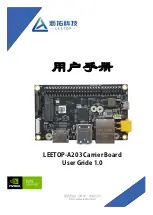
background image

PCIe-XPIMC-Carrier

XMC/PMC/PIM Carriers for PCIe

Hardware Manual

to Product V.2100.01,  V.2100.02

PCIe-XPIMC-Carrier

Hardware Manual • Doc. No.: V.2100.21 / Rev. 1.2

Page 1 of 27


                                          esd electronic system design gmbh
             Vahrenwalder Str. 207 • 30165 Hannover • Germany
                                                                   http://www.esd.eu   
Phone: +49 (0) 511 3 72 98-0 • Fax: +49 (0) 511 3 72 98-68

Summary of Contents for PCIe-XPIMC-Carrier

Page 1: ...re Manual to Product V 2100 01 V 2100 02 PCIe XPIMC Carrier Hardware Manual Doc No V 2100 21 Rev 1 2 Page 1 of 27 esd electronic system design gmbh Vahrenwalder Str 207 30165 Hannover Germany http www esd eu Phone 49 0 511 3 72 98 0 Fax 49 0 511 3 72 98 68 ...

Page 2: ...ghts to this documentation are reserved by esd Distribution to third parties and reproduction of this document in any form whole or in part are subject to esd s written approval 2012 esd electronic system design gmbh Hannover esd electronic system design gmbh Vahrenwalder Str 207 30165 Hannover Germany Phone 49 511 372 98 0 Fax 49 511 372 98 68 E Mail info esd eu Internet www esd eu Trademark Noti...

Page 3: ...n the description of the facts only Revision Chapter Changes versus previous version Date 1 0 First release 2011 11 18 1 1 Added new Safety Instructions 2012 08 14 2 1 Add new graphic 8 Added Declaration of Conformity 1 2 2 1 Updated PCB top view graphic 2012 11 26 8 Updated chapter Declaration of Conformity 10 Updated chapter Order Information Technical details are subject to change without furth...

Page 4: ...e XPIMC Carrier in order to discharge the static electricity from your body Qualified Personal This documentation is directed exclusively towards personal qualified in control and automation engineering The installation and commissioning of the product may only be carried out by qualified personal which is authorized to put devices systems and electric circuits into operation according to the appl...

Page 5: ... PMC XMC Interface 14 6 4 PIM 14 6 5 Power Supply Fan and Monitoring 15 7 Connector Assignments 16 7 1 J0 PIM Connector 16 7 2 J1 PMC XMC Connector 17 7 3 J2 PMC XMC Connector 18 7 4 J4A PMC XMC I O and J4B PIM I O Connectors 19 7 5 J15 XMC PCIe Connector 20 7 6 X2 PIM JTAG Connector 21 7 7 X3 PIM Test Signals 22 7 8 X4 Special P0 Signals 23 7 9 Option X5A B Aux Power 12V 24 8 Declaration of Confo...

Page 6: ...12V power rail For extreme high power applications an external power source 12V can optionally be installed The 12V auxiliary connector Aux Power is doubled IN OUT to allow daisy chaining multiple carriers on huge PCIe backplanes The carrier board is available in two versions Normal forward version the PIM slot is placed at the slot bracket side and the PMC XMC is oriented towards the system s cen...

Page 7: ...PCB View with Connectors 2 PCB View with Connectors 2 1 Normal Version Figure 2 PCB top view normal version PCIe XPIMC Carrier Hardware Manual Doc No V 2100 21 Rev 1 2 Page 7 of 27 ...

Page 8: ... Figure 2 The signal assignment of these connectors is described from page 16 The jumpers PROT and FAN are positioned between the connectors X4 and X3 Figure 3 Component placement specification of PCIe XPIMC reverse Carrier The reverse version has the PMC XMC and PIM sites swapped so that the PMC XMC bezel is accessible via the slot bracket see Figure 3 The position of the connectors J0 J1 J2 J4A ...

Page 9: ...PCB View with Connectors Figure 4 Position of connectors and pins of PCIe XPIMC reverse Carrier detail PCIe XPIMC Carrier Hardware Manual Doc No V 2100 21 Rev 1 2 Page 9 of 27 ...

Page 10: ...0 33MHz PCI Bus forced to 33 MHz operation speed is selected by PMC s M66EN signal not installed JP500 Jumpers with three male contacts PCIe and PROT These jumpers can be not installed or installed to POS A or POS B Name Jumper POS A Jumper POS B Jumper Not Installed Default Jumper Name in PCB PROT full protection enabled fan and temperature 1 only temperature observation protection disabled POS A...

Page 11: ...ected to mains disconnect the power supply via the safety fuse and make sure that the fuse cannot switch on again unintentionally i e with caution label Danger Never carry out work while power supply voltage is switched on 5 Open the case 6 Insert the PCIe XPIMC Carrier board into the selected PCIe slot Carefully push the board down until it snaps into place It is strongly recommended to install a...

Page 12: ...dicator State Description LED name in schematic diagram Error red Fan or Temperature Error off normal operation LED1 on fan or temperature error condition The LED behavior is uneffected by PROT jumper status Table 1 Description of LED Page 12 of 27 Hardware Manual Doc No V 2100 21 Rev 1 2 PCIe XPIMC Carrier ...

Page 13: ...or 6x19 pin J4B PIM I O PMC connector 64 pin J0 PIM Power JTAG Test Special PMC connector 64 pin X2 JTAG interface Molex 87832 1420 2x7 pin 2mm X3 Test signals 2 x 5 2 54 mm 2 row strip connector angled X4 Clock ODU Flakafix Series 511 or similar DIN41651 angled 14 pole engagement hooks X5a b Aux Power 12V in out 2 x Molex MicroFit 2 x 2 pole part 0430450400 0430450401 Temperature range 0 C 50 C a...

Page 14: ...n of the PCIe jumper Standard PMC IEEE Std 1386 2001 IEEE 1386 1 2001 XMC VITA 42 10 PMC XMC card size one single size module Signal voltage level PMC Universal 3 3V PCI signalling with 5 V tolerance Bus system XMC PCI Express Connectors J1 PMC XMC Power PCI J2 PMC XMC Power PCI J4a PMC XMC I O J15 XMC PCIe Table 4 Data of PMC interface 6 4 PIM Number 1 Standard acc to Vita 36d0 1 PIM card size on...

Page 15: ...ion the 12V connection to the card edge has to be disconnected by removing 0 Ohm resistors See block diagram for details on internal power supply rails Figure 1 Over current protection none all supply rails are short circuit protected Thermal protection 2x DS1631A under PMC XMC site The upper threshold is programmed to 60 C Fan placement fan is placed below PMC XMC site Fan type Sunon 40mm x 40mm ...

Page 16: ...c 27 28 DPSG 3 N GND 29 30 DPSG 3 P n c 31 32 n c n c 33 34 GND PM T1 35 36 DPSG 4 N 5V 37 38 DPSG 4 P PM T2 39 40 n c PM T3 41 42 3 3V PM T4 43 44 DPSG 5 N GND 45 46 DPSG 5 P n c 47 48 n c n c 49 50 GND PM T5 51 52 TIME_N 5V 53 54 TIME_P PM T6 55 56 n c PM T7 57 58 3 3V PM T8 59 60 n c 12V 61 62 SCL n c 63 64 SDA Note SCL SDA are connected to any I C capable component on the carrier This includes...

Page 17: ...23 24 GND GND 25 26 PCI C BE 3 P AD22 27 28 P AD21 P AD19 29 30 5V 3 3V 31 32 P AD17 PCI FRAME 33 34 GND GND 35 36 PCI IRDY PCI DEVSEL 37 38 5V GND 39 40 PCI LOCK 3 3 V via 3 3 kΩ 41 42 3 3 V via 3 3 kΩ PCI PAR 43 44 GND 3 3V 45 46 P AD15 P AD12 47 48 P AD11 P AD9 49 50 5V GND 51 52 PCI C BE 0 P AD6 53 54 P AD5 P AD4 55 56 GND 3 3V 57 58 P AD3 P AD2 59 60 P AD1 P AD0 61 62 5V GND 63 64 3 3 V via 3...

Page 18: ...2 P AD26 P AD24 23 24 3 3V P IDSEL0 25 26 P AD23 3 3V 27 28 P AD20 P AD18 29 30 GND P AD16 31 32 PCI C BE2 GND 33 34 P IDSEL1 PCI TRDY 35 36 3 3V GND 37 38 PCI STOP PCI PERR 39 40 GND 3 3V 41 42 PCI SERR PCI C BE1 43 44 GND P AD14 45 46 P AD13 PCI M66EN 47 48 P AD10 P AD8 49 50 3 3V P AD7 51 52 PCI REQ1 3 3V 53 54 PCI GNT1 n c 55 56 GND n c 57 58 n c GND 59 60 n c 3 3 V via 3 3 kΩ 61 62 3 3V GND 6...

Page 19: ...nectors The signal assignments of the I O connectors J4A and J4B are identical The signal pins of the connectors J4A and J4B are 1 1 connected internally So signals are only passed through PCIe XPIMC Carrier Hardware Manual Doc No V 2100 21 Rev 1 2 Page 19 of 27 ...

Page 20: ...GND 12V 7 n c n c 3 3V n c n c 5V 8 GND GND JTAG TD2 GND GND 12V 9 n c n c n c n c n c 5V 10 GND GND JTAG TDO GND GND GND 11 PEX IDATA0 P PEX IDATA0 N n c n c n c 5V 12 GND GND GND GND GND LC XMC_ PRSNT 13 n c n c 3 3V AUX n c n c 5V 14 GND GND 3 3V GND GND SDA 15 n c n c n c n c n c 5V 16 GND GND GND GND GND SCL 17 n c n c n c n c n c n c 18 GND GND n c GND GND n c 19 PEX RCLK0 P PEX RCLK0 N n c ...

Page 21: ...on connector view Pin 13 1 14 2 Pin Assignment Signal Pin Pin Signal GND 1 2 3 3V GND 3 4 PIM TMS GND 5 6 PIM TCK GND 7 8 PIM TDO GND 9 10 PIM TDI GND 11 12 n c GND 13 14 PIM TRST Note All JTAG signals are directly routed to the PIM J0 connector PCIe XPIMC Carrier Hardware Manual Doc No V 2100 21 Rev 1 2 Page 21 of 27 ...

Page 22: ...led Pin Position connector view Pin 9 1 10 2 PCB side Pin Assignment Signal Pin Pin Signal GND 1 2 PM T1 PM T2 3 4 PM T3 PM T4 5 6 PM T5 PM T6 7 8 PM T7 PM T8 9 10 3 3V Note All test signals are directly routed to the PIM J0 connector Page 22 of 27 Hardware Manual Doc No V 2100 21 Rev 1 2 PCIe XPIMC Carrier ...

Page 23: ...G 1 N 1 2 DPSG 1 P DPSG 2 N 3 4 DPSG 2 P DPSG 3 N 5 6 DPSG 3 P GND 7 8 GND DPSG 4 N 9 10 DPSG 4 P DPSG 5 N 11 12 DPSG 5 P TIME_N IRIG B digital 13 14 TIME_P IRIG B digital Note 1 All signals are routed for differential signalling Note 2 All signal pairs are terminated by a series network 100R 1nF Note 3 All test signals are directly routed to the PIM J0 connector PCIe XPIMC Carrier Hardware Manual...

Page 24: ...X5B are assigned with the same signals Pin Assignment Signal Pin Pin Signal GND 4 3 GND 12V_aux 2 1 12V_aux X5A B are are optional and not installed per default Per default the 12 V power supply voltage is supplied via the card edge connector When X5A B are used to supply the board the 12V rail on the card edge must be disconnected Please contact esd for instructions Page 24 of 27 Hardware Manual ...

Page 25: ...Declaration of Conformity 8 Declaration of Conformity PCIe XPIMC Carrier Hardware Manual Doc No V 2100 21 Rev 1 2 Page 25 of 27 ...

Page 26: ...on Rev 1 1 2 PCI local bus specification Rev 3 0 3 PMC IEEE 1386 4 XMC specification Vita 42 0 5 PIM specification Vita 36 199X 6 PCIe electromechanical specification Rev 2 0 Page 26 of 27 Hardware Manual Doc No V 2100 21 Rev 1 2 PCIe XPIMC Carrier ...

Page 27: ...sh and usually in German as well For availability of English manuals see table below Please download the manuals as PDF documents from our esd website www esd eu for free Manuals Order No PCIe XPIMC Carrier ME Hardware manual in English V 2100 21 Table 7 Available manuals Printed Manuals If you need a printout of the manual additionally please contact our sales team sales esd eu for a quotation Pr...

Reviews: