SERVICE MANUAL
When servicing the deck
mechanism, refer to MK12.5 Deck
Mechanism Section.
Deck Mechanism Part No.:
N2260FL
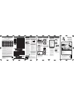
Main Section
I
Specifications
I
Preparation for Servicing
I
Adjustment Procedures
I
Schematic Diagrams
I
CBA’s
I
Exploded Views
I
Parts List
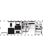
DVD RECORDER &
VIDEO CASSETTE RECORDER
POWER
REW
F.FWD
PLAY
RECORD
CHANNEL
DUBBING
SELECT
STOP
PLAY
RECORD
S-VIDEO
VIDEO
L - AUDIO - R
OPEN/CLOSE
STOP/EJECT
VCR
DVD
SELECT
EWR20V4
Summary of Contents for EWR20V4
Page 14: ...1 6 1 E9400IB OPERATING CONTROLS AND FUNCTIONS ...
Page 15: ...1 6 2 E9400IB ...
Page 91: ...EWR20V4 E9400UD 2004 04 19 ...