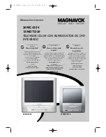
background image

SERVICE MANUAL

13" COLOR TV/VCR COMBINATION

EWC1303A

Main Section

I

 Specifications

I

 Preparation for Servicing

I

 Adjustment Procedures

I

 Schematic Diagrams

I

 CBA’s

I

 Exploded Views

I

 Parts List

When servicing the deck 
mechanism, refer to MK12.5 Deck 
Mechanism Section.

Deck Mechanism Part No.: 
N2226FT

Summary of Contents for EWC1303A

Page 1: ...303A Main Section I Specifications I Preparation for Servicing I Adjustment Procedures I Schematic Diagrams I CBA s I Exploded Views I Parts List When servicing the deck mechanism refer to MK12 5 Deck Mechanism Section Deck Mechanism Part No N2226FT ...

Page 2: ...injury to service personnel The possibility exists that improper ser vice methods may damage the equipment It also is important to understand that these CAUTIONS and NOTICES ARE NOT EXHAUSTIVE Funai could not possibly know evaluate and advice the service trade of all conceivable ways in which service might be done or of the possible hazardous consequences of each way Consequently Funai has not und...

Page 3: ...ouble Indicator 1 7 7 Power Supply Trouble Shooting Guide 1 7 9 Schematic Diagrams CBA s and Test Points 1 8 1 Waveforms 1 9 1 Wiring Diagram 1 10 1 System Control Timing Charts 1 11 1 IC Pin Function Descriptions 1 12 1 Lead Identifications 1 13 1 Cabinet Exploded Views 1 14 1 Packing Exploded Views 1 14 3 Mechanical Parts List 1 15 1 Electrical Parts List 1 16 1 Main Section I Specifications I P...

Page 4: ...10 3 High Voltage kV 22 Description Condition Unit Nominal Limit 1 Misconvergence Center m m 0 3 Corner m m 1 5 Side m m 1 2 2 Tint Control Range deg 30 3 Contrast Control Range dB 12 8 4 Brightness APL 100 ft L 55 40 5 Color Temperature K 9200 Description Condition Unit Nominal Limit 1 Horizontal Resolution R P Line 230 200 2 Jitter Low R P µS 0 05 0 2 3 S N Chroma AM SP R P dB 38 33 PM SP R P dB...

Page 5: ...rop slightly below these specifications Limit specifications represent the abso lute worst condition that still might be considered acceptable In no case should a unit fail to meet limit specifica tions Description Condition Unit Nominal Limit 1 Audio Output Power Max R P W 1 0 0 8 2 Audio S N W LPF R P dB 40 36 3 Audio Distortion W LPF R P 3 0 5 0 4 Audio Freq Response 10dB Ref 1KHz 200Hz R P 8kH...

Page 6: ...ongs tied together and touch the other ohmme ter lead in turn to each tuner antenna input ex posed terminal screw and if applicable to the coaxial connector If the measured resistance is less than 1 0 megohm or greater than 5 2 mego hm an abnormality exists that must be corrected before the instrument is returned to the customer Repeat this test with the instrument AC switch in the off position d ...

Page 7: ...d to the ground side of the AC power source To confirm that the AC power plug is inserted correctly with an AC volt meter measure between the chassis and a known earth ground If a voltage reading in excess of 1 0V is obtained remove and reinsert the AC power plug in the opposite polarity and again measure the voltage potential between the chassis and a known earth ground b Some TV receiver chassis...

Page 8: ...not contact sharp edged or pointed parts H When a power cord has been replaced check that 5 6 kg of force in any direction will not loosen it I Also check areas surrounding repaired locations J Use care that foreign objects screws solder drop lets etc do not remain inside the set K Crimp type wire connector When replacing the power transformer in sets where the connections between the power cord a...

Page 9: ...r cord plug prongs and externally exposed accessible parts RF terminals antenna terminals video and audio input and output terminals microphone jacks earphone jacks etc Measuring Method Power ON Insert load Z between B earth ground power cord plug prongs and exposed accessible parts Use an AC voltmeter to measure across both terminals of load Z See Fig 2 and following table Table 2 Leakage current...

Page 10: ...reused Always use a new part Pb Free Solder PbF When soldering be sure to use the Pb free solder Replacement Procedures for Leadless Chip Components The Following Procedures are Recom mended for the Replacement of the Lead less Components Used in this Unit 1 Preparation for replacement a Soldering Iron Use a pencil type soldering iron less than 30 watts b Solder Eutectic solder Tin 63 Lead 37 is r...

Page 11: ... lands under the IC when removing it 1 Removal With Hot Air Flat Pack IC Desoldering Machine a Prepare the Hot Air Flat Pack IC Desoldering Machine then apply hot air to Flat Pack IC about 5 6 seconds Fig S 1 1 b Remove the Flat Pack IC with tweezers while applying the hot air With Soldering Iron a Using desoldering braid remove the solder from all pins of the Flat Pack IC When you use solder flux...

Page 12: ...for installation Then pre solder the four corners of the Flat Pack IC See Fig S 1 7 c Solder all pins of the Flat Pack IC Make sure that none of the pins have solder bridges Fig S 1 1 Fig S 1 2 Hot air Flat Pack IC Desoldering Machine CBA Flat Pack IC Tweezers Masking Tape Fig S 1 3 Flat Pack IC Desoldering Braid Soldering Iron Fig S 1 4 Fine Tip Soldering Iron Sharp Pin Fig S 1 5 To Solid Mountin...

Page 13: ... static electricity that may be charged on the body Ground for Work Bench Be sure to place a conductive sheet or copper plate with proper grounding 1MΩ on the work bench or other surface where the semiconductors are to be placed Because the static electricity charge on the clothing will not escape through the body grounding band be careful to avoid contacting semiconductors to clothing Fig S 1 7 P...

Page 14: ...not be oper ated automatically Preparing 2 1 To eject the tape press the STOP EJECT button on the unit or Remote Control 2 When you want to record during the Service mode press the Rec button while depressing SW211 REC SAFETY SW on the Main CBA Key Adjustment Mode MENU Picture adjustment mode Press the MENU button to change from BRT Bright CNT Contrast COL Color TNT Tint and V T Press CH UP DOWN k...

Page 15: ... 5 Refer to the following Reference Notes in the Table Reference Notes in the Table 1 Removal of the Rear Cabinet Remove screws 4 S 1 and S 2 Caution Discharge the Anode Lead of the CRT with the CRT Ground Wire before removing the Anode Cap 2 Removal of the Tray Chassis Discharge the Anode Lead of the CRT with the CRT Ground Wire before removing the Anode Cap Disconnect the following Anode Cap CN5...

Page 16: ...1 5 2 T5553DC S 1 1 REAR CABINET S 1 S 2 Fig 1 Fig 2 1 REAR CABINET S 1 S 2 S 1 S 1 S 1 ...

Page 17: ...1 5 3 T5553DC Fig 3 2 TRAY CHASSIS 3 DECK UNIT S 3 S 3 S 3 4 MAIN CBA S 6 S 5 S 4 S 6 S 6 S 6 S 7 ...

Page 18: ...1 5 4 T5553DC Fig 4 S 8 S 8 S 8 S 8 ANODE CAP 5 CRT CRT CBA ...

Page 19: ...CL502A CL501A SCREEN CN505 CN801 CN601 CN571 FOCUS CRT CBA AC CORD CL403 FE HEAD CYLINDER ASSEMBLY ACE HEAD ASSEMBLY CAPSTAN MOTOR DECK UNIT MAIN CBA CL401 CL502B CL201 CL402 CL501B CRT ANODE GND TO SPEAKER TO DEGAUSS COIL ...

Page 20: ...oces sor with a jumper wire Note The remote control with the unit cannot be used as service remote control unit How to Set up the Service mode Service mode 1 Use the service remote control unit 2 Turn the power on 3 Press WAKE UP SLEEP button on the service remote control unit 1 DC 105V B Adjustment Purpose To obtain correct operation Symptom of Misadjustment The picture is dark and unit does not ...

Page 21: ...unter display is closest to 15 734kHz 300Hz 6 Turn the power off and on again 3 2 C Trap Adjustment Purpose To get minimum leakage of the color signal carrier Symptom of Misadjustment If C Trap Adjustment is incorrect stripes will appear on the screen Note J271 B Out Main CBA 1 Connect Oscilloscope to J271 2 Input a color bar signal from RF input Enter the Service mode See page 1 4 1 3 Press 0 but...

Page 22: ...the ser vice remote control unit seven times to show C ANG on the display 3 Y DL Time TV Adjustment Select 2 by pressing CH o p buttons on the service remote control Y DL Time EXT Adjustment Select 2 by press ing CH o p buttons on the service remote con trol Y SW LPF Adjustment Select 1 by pressing CH o p buttons on the service remote control Black Stretch Off Adjustment Select OFF by pressing CH ...

Page 23: ...the top and bottom of the monoscope pattern are equal to each other 6 H Shift Adjustment Purpose To obtain correct horizontal position and size of screen image Symptom of Misadjustment Horizontal position and size of screen image may not be properly displayed 1 Enter the Service mode See page 1 4 1 Press 8 button on the remote control unit and select H P mode 2 Input monoscope pattern 3 Press CH o...

Page 24: ...the horizontal line becomes white 9 Input the White Raster Signal from Video In 10 Choose CUT OFF DRIVE mode then press 4 Adjust the RED DRIVE as needed with the CH o p buttons to get the following value X 286 Y 294 11 Choose CUT OFF DRIVE mode then press 5 Adjust the BLUE DRIVE as needed with the CH o p buttons to get the following value X 286 12 Turn the power off and on again 8 Sub Brightness A...

Page 25: ...microcomputer The following 2 adjustments normally are not attempted in the field They should be done only when replacing the CRT then adjust as a preparation 12 Purity Adjustment Purpose To obtain pure color Symptom of Misadjustment If Color Purity Adjust ment is incorrect large areas of color may not be properly displayed This becomes RED COLOR if push 7KEY with a service mode 1 Set the unit fac...

Page 26: ...s at the center of the screen by rotating RB G C P Magnet See Fig 8 4 Fix the C P Magnets by tightening the Ring Lock 5 Remove the DY Wedges and slightly tilt the Deflec tion Yoke horizontally and vertically to obtain the best overall convergence 6 Fix the Deflection Yoke by carefully inserting the DY Wedges between CRT and Deflection Yoke Test point Adj Point Mode Input C P Magnet RB C P Magnet R...

Page 27: ... KEY SWITCH KEY SWITCH SW201 SW204 SW206 SCL MEMORY SDA 6 5 REC LED 22 REC LED 23 P DOWN 84 P ON H P DOWN P ON H 31 D204 REC AL 5V LD SW 1 I 2 C OPEN 45 71 SW212 LD SW CS 7 TO POWER SUPPLY BLOCK SW205 SW207 SW210 SDA SCL TO CHROMA TUNER BLOCK SDA SCL IC202 WF3 2 2 CTL 1 1 CTL M M LOADING MOTOR CYLINDER ASSEMBLY CAPSTAN MOTOR SENSOR CBA ST SENSOR SENSOR CBA END SENSOR DRUM MOTOR PG SENSOR CL201 C F...

Page 28: ...IGNAL MODE SP REC 57 QV QH 6dB AMP TO SERVO SYSTEM CONTROL BLOCK TO SERVO SYSTEM CONTROL BLOCK RF SW RF SW 59 V ENV TP202 DV SYNC DV SYNC 53 24 YCA SCLK 36 37 39 34 Q402 BUFFER 54 YCA SOUT 55 YCA CS SERIAL I F VCA CLAMP 69 70 SP HEAD AMP 72 73 74 V ENV ROTA C ROT RF SW WF1 JK701 FRONT V IN 42 30 TO CHROMA TUNER BLOCK 32 TU VIDEO LINE VIDEO WF4 TUNER LINE Q401 TP301 V OUT BUFFER VIDEO WF5 TP402 V E...

Page 29: ...N801 CL802 SP MUTE TU AUDIO TO CHROMA TUNER BLOCK TP401 A OUT AUDIO HEAD AC HEAD ASSEMBLY A COM A PB REC CL402 AUDIO ERASE HEAD AE H AE H FE H 2 1 FE H FE H GND FULL ERASE HEAD CL403 3 4 6 FE HEAD UNIT SERIAL I F AUDIO ATT SDA SCL TO SERVO SYSTEM CONTROL BLOCK TUNER REC AMP AUTO BIAS LINE AMP MUTE P R ALC TUNER LINE D REC H A MUTE TO SERVO SYSTEM CONTROL BLOCK WF8 32 EQ AMP SP LP ON 5 24 14 15 26 ...

Page 30: ...RVO SYSTEM CONTROL BLOCK REC VIDEO SIGNAL PB VIDEO SIGNAL Mode SP REC REC AUDIO SIGNAL WF18 WF17 WF10 WF11 TP302 AFC 56 CV IN 4 MAIN CBA 18 34 35 8 9 31 13 10 11 12 15 14 4 5 3 2 40 41 16 6 20 25 23 CHROMA TRAP SERIAL I F INTELLIGENT MONITORING CHROMA BPF SYNC SEPARATION LUMA SIGNAL PROCESS CIRCUIT CHROMA SIGNAL PROCESS CIRCUIT H SYNC PROCESS CIRCUIT V SYNC PROCESS CIRCUIT OSD MIX RBG MATRIX BLIGH...

Page 31: ... F B T ANODE FOCUS SCREEN MAIN CBA CRT CBA R G B HEATER ANODE GND V501 CRT GND FOCUS SCREEN JK501 CN505 CL501A CL501B REC VIDEO SIGNAL PB VIDEO SIGNAL CN571 TO CHROMA TUNER BLOCK FOCUS VR SCREEN VR TO CHROMA TUNER BLOCK CL502B B TO POWER SUPPLY BLOCK DEF B H OUTPUT V RAMP NF 5 4 3 1 WF12 WF15 WF14 WF16 WF13 RED AMP Mode SP REC CL502A VCC 6 7 1 3 2 5 1 5 3 4 6 9 7 10 8 11 S F HV 3 3 HEATER 1 1 160V...

Page 32: ...N 12V AL 5V P ON H TO PIN31 OF IC201 5V REG 5V REG 5V REG 5V REG 8V REG IC602 Q608 Q611 Q610 Q609 Q612 5 7V REGULATOR IC301 30 27 B DEF B HOT CIRCUIT BE CAREFUL FOR CONTINUED PROTECTION AGAINST RISK OF FIRE REPLACE ONLY WITH SAME TYPE 4 A 125V FUSE CAUTION ATTENTION UTILISER UN FUSIBLE DE RECHANGE DE MÊME TYPE DE 4A 125V 4A 125V CAUTION Fixed voltage or Auto voltage selectable power supply circuit...

Page 33: ...ately turn OFF the POWER MONITOR and switch over the Mechanical Malfunction mode with POWER OFF Shall not unload To return from this mode shall become possible only by POWER Key as in the case of the Mechan ical Malfunction However the POWER SAFETY 2 function shall be disabled during 500 msec right after the P ON H turns ON 2 POWER SAFETY 3 If P SAFETY 3 port becomes continuously 2 5V or over for ...

Page 34: ...it keeps the function according to its mode 4 Countermeasure for CASSETTE LOADING Mal function a CASSETTE IN operating Malfunction If LD SW does not go to SB position after a lapse of 5 sec or more from the CASSETTE insertion start the unit starts the CASSETTE OUT opera tion After switch over to CASSETTE OUT operation and then a laps of 5 sec or more from the CASSETTE OUT operation start if LD SW ...

Page 35: ...onitors current will do Read directions below before power is added Repair method 1 Power must be off Short circuit in the secondary side check diode D613 D614 D616 D617 and D618 switching transistor Q601 control transistor Q602 diode and resistor replace as necessary Disconnect 105V diode D613 25V diode D614 8V diode D616 12V diode D617 12V diode D618 and Check the load continuity of 105V line 25...

Page 36: ... parts then if necessary replace with factory originals R602 is open or not Q601 Q602 D607 D608 and D611 are short or not Repair method 3 The feedback circuit which is monitored by the output of D613 105V may not work and this may be regarded as a possible cause remove IC601 Photo Coupler diode D620 and transistor Q604 check for defects Repair method 4 Check control circuitly which is connecting t...

Page 37: ...dentified by the mark in the schematic diagram and the parts list Before replacing any of these components read the parts list in this manual carefully The use of substitute replacement parts that do not have the same safety characteristics as speci fied in the parts list may create shock fire or other hazards Capacitor Temperature Markings Capacitors and transistors are represented by the fol low...

Page 38: ...ed units use only original replacement parts which are listed with their part numbers in the parts list section of the service manual 4 Wire Connectors 1 Prefix symbol CN means connector can disconnect and reconnect 2 Prefix symbol CL means wire solder holes of the PCB wire is soldered directly 5 Note Mark is a leadless chip component 6 Mode SP REC 7 Voltage indications for PLAY and REC modes on t...

Page 39: ...1 C2 C3 C4 D1 D2 D3 D4 E1 E2 E3 E4 F1 F2 F3 F4 Main 1 5 Schematic Diagram 1 8 3 1 8 4 T5553SCM1 MAIN 1 5 Ref No Position IC201 C 2 IC202 D 1 Q205 B 1 Q206 D 3 CL201 F 4 TP201 B 4 TP202 B 2 ICS TRANSISTORS CONNECTOR TEST POINTS ...

Page 40: ...gnal PB Video Signal PB Audio Signal Main 2 5 Schematic Diagram 1 8 5 1 8 6 T5553SCM2 MAIN 2 5 Ref No Position IC401 H 2 IC801 K 4 Q401 K 2 Q402 K 3 Q871 H 2 Q872 H 1 Q873 G 1 Q874 G 1 Q875 H 1 CL401 G 3 CL402 L 1 CL403 G 1 CN801 K 4 TP301 K 2 TP401 J 1 TP402 J 1 TRANSISTORS TEST POINTS CONNECTORS ICS ...

Page 41: ...1 P2 P3 P4 Q1 Q2 Q3 Q4 R1 R2 R3 R4 REC Video Signal REC Audio Signal PB Video Signal PB Audio Signal Main 3 5 Schematic Diagram 1 8 7 1 8 8 T5553SCM3 MAIN 3 5 Ref No Position IC001 Q 2 IC301 M 2 Q301 N 1 TP302 O 1 ICS TRANSISTOR TEST POINT ...

Page 42: ...he power supply circuit are not defective before you connect the AC plug to the AC power supply Otherwise it may cause some components in the power supply circuit to fail VOLTAGE CHART Power off mode Ref No 1 4 IC601 11 0 16 0 Ref No IC602 Ref No Q601 Ref No Q602 Q604 Q605 Q606 Q607 Q608 Q609 Q610 Q611 Q612 Q613 1 4 0 1 9 0 8 2 0 7 0 6 5 B 0 7 8 0 3 0 G 1 8 5 6 3 0 5 1 3 0 8 8 0 3 0 8 2 5 1 0 2 10...

Page 43: ... Signal 1 8 11 1 8 12 T5553SCM5 Main 5 5 CRT Schematic Diagram MAIN 5 5 Ref No Position IC551 Y 3 Q571 AA 2 Q572 Z 3 Q591 Z 2 CL501B BB 3 CL502B BB 2 CN571 Z 3 CONNECTORS IC TRANSISTORS CRT Ref No Position Q511 CC 2 Q521 CC 2 Q531 CC 2 CL501A BB 3 CL502A BB 2 CN505 DD 2 TRANSISTORS CONNECTORS ...

Page 44: ... Top View BT5500F01011 CAUTION Fixed voltage or Auto voltage selectable power supply circuit is used in this unit If Main Fuse F601 is blown check to see that all components in the power supply circuit are not defective before you connect the AC plug to the AC power supply Otherwise it may cause some components in the power supply circuit to fail 1 8 13 1 8 14 BHB300F01014 A BHB300F01014 B MAIN CB...

Page 45: ...IABLE ISOLATION TRANSFORMER IS REQUIRED CAUTION FOR CONTINUED PROTECTION AGAINST RISK OF FIRE REPLACE ONLY WITH SAME TYPE 4A 125V FUSE ATTENTION UTILISER UN FUSIBLE DE RECHANGE DE MÊME TYPE DE 4A 125V 4A 125V NOTE The voltage for parts in hot circuit is measured using hot GND as a common terminal CAUTION Fixed voltage or Auto voltage selectable power supply circuit is used in this unit If Main Fus...

Page 46: ... WF16 Q521 Collector WF15 Q511 Collector WF14 CRT CBA Top View CRT CBA Bottom View 1 8 17 1 8 18 BT5500F01011 CRT CBA Ref No Position Q511 B 1 Q521 B 1 Q531 A 1 CL501A A 1 CL502A B 1 CN505 B 2 TRANSISTORS CONNECTORS ...

Page 47: ...0 µ sec IC401 PIN 32 Upper WF6 Lower WF1 1DIV 0 2V 2DIV 5V 5msec TP402 V ENV WF5 1DIV 0 5V 20 µ sec TP301 V OUT WF8 1DIV 0 5V 0 5msec TP401 A OUT WF7 1DIV 0 2V 0 5msec IC001PIN 7 WF9 1DIV 0 5V 0 5msec IC401 PIN 9 WF11 1DIV 1V 20 µ sec IC301 PIN41 WF10 1DIV 2V 5msec IC301 PIN 9 WF12 1DIV 200V 20 µ sec Q571 COLLECTOR WF17 WF18 1DIV 1V 20 µ sec IC201 PIN 58 1DIV 1V 5msec IC201 PIN 59 WF14 1DIV 20V 20...

Page 48: ... AUDIO ERASE HEAD M LOADING MOTOR CYLINDER ASSEMBLY CL201 CAPSTAN MOTOR M DRUM MOTOR PG SENSOR CL402 1 FE H GND 2 FE H 1 P ON 12V 2 P ON 5V 2 3 C FG 4 C F R 5 C CONT 6 FG GND 7 LD CONT 8 D CONT 9 D PFG 10 M GND 11 D L 12V 12 D L 15V 6 AE H 5 AE H FE H 4 A COM 3 A PB REC 2 CTL 1 CTL 1 SPEAKER 2 SP GND 1 GND 2 RED 3 GREEN 4 BLUE 1 GND 2 RED 3 GREEN 4 BULE 1 160V 2 GND 3 HEATER 1 160V 2 GND 3 HEATER ...

Page 49: ...V LD REV 0 2S 0 5S PIN NO CL EJ SS SS AU AU TL LD SW CL SS LD CONT C DRIVE Z ON ON C F R DRUM ROTATION P ON A MUTE H D REC H D PB H PAUSE ON PAUSE PAUSE ON PAUSE OFF PAUSE OFF AU AL AU SF SM EJ AU RS SF SM TL FB AL SB 1 82 66 31 65 44 POWER OFF STOP PLAY RS FS PLAY STILL STOP PLAY DISPLAY SB TL SB FB SM SM SF AL AL RS AU AL SM 0 8S 0 2S 0 3S 1 0S 0 2S 100mS NTSC after channel setting 620mS PAL 1 0...

Page 50: ...OP A LD REV FF LD REV LD REV LD FWD LD FWD LD FWD LD FWD LD FWD LD FWD LD FWD REC PAUSE REC REC REW LD REV LD REV LD REV LD REV LD REV LD REV LD REV PAUSE REC or PAUSE STOP EJECT STOP EJECT STOP EJECT 2 STOP A FF STOP A REW STOP A REC PAUSE PAUSE or REC STOP A EJECT STOP FF STOP REW STOP REC REC REC PAUSE STOP TL TL SM SM SF SF AL AL SM AL AL AL AU AU SM TL SB EJ RS RS SM SM SF FB SM AU AU SS SS S...

Page 51: ...d 26 FM TV SW FM TV SW Signal 27 NU Not Used 28 NU Not Used 29 NU Not Used 30 NU Not Used 31 OUT P ON H Power On Signal at High 32 NU Not Used 33 IN REC SAFETY Record Protection Tab Detection 34 IN RESET System Reset Signal Reset L 35 IN XC IN Sub Clock 32 kHz 36 OUT XC OUT Sub Clock 32 kHz 37 TIMER 5V Vcc 38 IN X IN Main Clock Input 39 OUT X OUT Main Clock Output 40 GND GND 41 OUT SPOT KILL Count...

Page 52: ...EL Take Up Reel Rotation Signal 81 NU Not Used 82 OUT LD CONT Loading Motor Control Signal 83 NU Not Used 84 IN P DOWN Power Voltage Down Detector Signal 85 NU Not Used 86 GND GND 87 IN C FG Capstan Motor Rotation Detection Pulse 88 GND GND AMP 89 NU Not Used 90 IN D PFG Drum Motor Pulse Generator 91 NU Not Used 92 OUT AMP VREF IN Standard Voltage Input 93 C C 94 IN OUT CTL CTL 95 IN OUT CTL CTL 9...

Page 53: ...Y TPE2 2SC2482 TPE6 2SC2785 F 2SC3468 D E AE BN1F4M T KTA1267 GR KTA1271 Y KTC3199 GR KTC3207 2SC1815 GR TPE2 2SC2120 O Y TPE2 2SC3331 T U KRA103M KTC3203 Y LA78040A 2SC5884000RF TT2138LS YB11 MID 32A22F PT204 6B 12 KA7805A KIA7805API LTV 817B F LTV 817C F PC817X6 M37762M8A 8D4GP 2SK3563 AN17811A M61275FP 61 M61113FP BR24C02F W CAT24WC02JI M24C02 WMN6 S Souce D Drain G Gate E Emitter C Collector B...

Page 54: ... 2 A1 4 A1 1 B1 TB21 TB7 L7 1B1 B3 TB2 TB24 TB24 TL3 TL3 B13 V501 1 L551 Details for L551 and surrounding parts SHINWHA TAPE SGT 730 WHITE SHINWHA TAPE SGT 730 BLACK V501 3 V501 2 L551 DG601 CL802 SP801 CLN551 A1X See Electrical Parts List for parts with this mark CRT CBA MAIN CBA W601 SCOTCH TAPE 880 V501 SENSOR CBA SENSOR CBA 1 14 1 1 14 2 T5553CEX ...

Page 55: ...1 14 3 T5553PEX Packing X3 X4 X2 TAPE X1 X7 X5 S2 S6 S3 S1 S4 FRONT S15 ...

Page 56: ...N0159UD N0159UD X4 DRY BATTERY R6P UM3 or XB0M451GH001 DRY BATTERY R6P AR 2PX or XB0M451HU002 DRY BATTERY R6P AR 2P X ICI or XB0M451HU003 DRY BATTERY SUNRISE R6SSE 2S or XB0M451MS002 DRY BATTERY R6P 2S XB0M451T0001 X5 ROD ANTENNA T5200UA or 0EMN01755 ROD ANTENNA L7720UA NTSC W COO or 0EMN00673 ROD ANTENNA T5000UA 0EMN01599 X7 SHEET RETURN STOP T4259UK 0EM406203A Note 1 V501 CRT HAS COUPLE OF SUBST...

Page 57: ... 20X10X1 2 XM05000BV001 CRT TYPE G L551 DEFLECTION YOKE LLBY00ZSY002 or LLBY00ZSY002 DEFLECTION YOKE KDY3GCE83X or LLBY00ZMS027 DEFLECTION YOKE CDY M1456S LLBY00ZQS008 V501 CRT A34JXV70X TCRT190THA02 V501 1 C P MAGNET JH225 FN 00 XM04000BV003 V501 2 WEDGE FT 00110W or XV10000T4001 WEDGE DB25SR XV10000D9001 V501 3 RUBBER MAGNET 20X10X1 2 XM05000BV001 Ref No Description Part No V501 CRT Type No V501...

Page 58: ... CZM1CZB0F103 C217 CHIP CERAMIC CAP MELF SL D 10pF 50V CZM1JDBSL100 C218 CHIP CERAMIC CAP CH J 15pF 50V CHD1JJBCH150 C219 CHIP CERAMIC CAP B K 0 01µF 50V CHD1JKB0B103 C220 ELECTROLYTIC CAP 220µF 6 3V M H7 CE0KMAVSL221 C221 CHIP CERAMIC CAP MELF F Z 0 01µF 16V CZM1CZB0F103 C222 CHIP CERAMIC CAP MELF Y K 2200pF 35V CZM1GKB0Y222 C223 CHIP CERAMIC CAP F Z 1µF 10V CHD1AZB0F105 C224 CHIP CERAMIC CAP MEL...

Page 59: ...00µF 25V M CE1EMZPTL102 C558 CERAMIC CAP AX B K 0 01µF 50V CA1J103TU011 C559 ELECTROLYTIC CAP 330µF 35V M or CE1GMASDL331 ELECTROLYTIC CAP 330µF 35V M CE1GMASTL331 C560 FILM CAP P 0 01µF 100V J CMA2AJS00103 Ref No Description Part No C572 P P CAP 0 33µF 200V J or CA2D334VC012 PP CAP 0 33µF 250V J CT2E334MS041 C574 ELECTROLYTIC CAP 4 7µF 250V M or CE2EMASDL4R7 ELECTROLYTIC CAP 4 7µF 250V M CE2EMAST...

Page 60: ...002 STRAIGHT PIN HEADER 2P 173981 2 1770258 DIODES D031 SWITCHING DIODE 1SS133 T 77 or QDTZ001SS133 SWITCHING DIODE 1N4148 NDTZ001N4148 D203 LED SIR 563ST3F P or QPQPS1R563ST LED SIR 563ST3F Q or QPQQS1R563ST Ref No Description Part No LED MIE 534A2 NPZZM1E534A2 D204 LED LTL 4214M1 or NPQZLTL4214M LED LAMP 333HT F45 50K or NPWK333HTF45 LED LAMP 333HT F45 50L or NPWL333HTF45 LED LAMP 333HT F45 50M ...

Page 61: ...638 SWITCHING DIODE 1SS133 T 77 or QDTZ001SS133 SWITCHING DIODE 1N4148 NDTZ001N4148 D640 SWITCHING DIODE 1SS133 T 77 or QDTZ001SS133 SWITCHING DIODE 1N4148 NDTZ001N4148 D641 ZENER DIODE MTZJT 7736A or QDTA00MTZJ36 Ref No Description Part No ZENER DIODE DZ 36BSAT265 NDTA00DZ36BS D643 SWITCHING DIODE 1SS133 T 77 or QDTZ001SS133 SWITCHING DIODE 1N4148 NDTZ001N4148 D646 SWITCHING DIODE 1SS133 T 77 or ...

Page 62: ... Description Part No RESISTORS R002 CHIP RES 1608 1 10W J 100 Ω RRXAJB5Z0101 R003 CHIP RES 1608 1 10W J 100 Ω RRXAJB5Z0101 R032 CHIP RES 1608 1 10W J 100 Ω RRXAJB5Z0101 R033 CHIP RES 1608 1 10W J 390k Ω RRXAJB5Z0394 R034 CHIP RES 1608 1 10W J 150 Ω RRXAJB5Z0151 R035 CHIP RES 1608 1 10W J 220k Ω RRXAJB5Z0224 R036 CHIP RES 1608 1 10W J 220k Ω RRXAJB5Z0224 R037 CHIP RES 1608 1 10W J 180 Ω RRXAJB5Z018...

Page 63: ...Z0395 R424 CHIP RES 1608 1 10W J 100k Ω RRXAJB5Z0104 R425 CHIP RES 1608 1 10W J 82k Ω RRXAJB5Z0823 Ref No Description Part No R426 CHIP RES 1608 1 10W J 2 2k Ω RRXAJB5Z0222 R427 CARBON RES 1 4W J 820 Ω RCX4JATZ0821 R428 CHIP RES 1608 1 10W J 680k Ω RRXAJB5Z0684 R429 CHIP RES 1608 1 10W J 1 2k Ω RRXAJB5Z0122 R431 CHIP RES 1608 1 10W J 8 2k Ω RRXAJB5Z0822 R432 CHIP RES 1608 1 10W J 1 8k Ω RRXAJB5Z01...

Page 64: ...51 CHIP RES 1608 1 10W J 22k Ω RRXAJB5Z0223 R852 CHIP RES 1608 1 10W J 3 3k Ω RRXAJB5Z0332 R853 CHIP RES 1608 1 10W J 2 2M Ω RRXAJB5Z0225 Ref No Description Part No R856 CARBON RES 1 4W J 22k Ω RCX4JATZ0223 R857 CHIP RES 1608 1 10W J 3 9k Ω RRXAJB5Z0392 R862 PCB JUMPER D0 6 P5 0 JW5 0T R863 CHIP RES 1608 1 10W J 1k Ω RRXAJB5Z0102 R864 CHIP RES 1608 1 10W J 22k Ω RRXAJB5Z0223 R865 CHIP RES 1608 1 1...

Page 65: ...0PPM or FXC355LDS001 X TAL 3 579545MHz 20PPM FXC355LCHE01 Ref No Description Part No Ref No Description Part No CRT CBA Consists of the following CAPACITORS C501 CERAMIC CAP B K 1000pF 2KV or CCD3DKP0B102 CERAMIC CAP B K 1000pF 2KV or CA3D102MR030 CERAMIC CAP B K 1000pF 2KV CCD3DKD0B102 C502 ELECTROLYTIC CAP 1µF 50V M or CE1JMASDL1R0 ELECTROLYTIC CAP 1µF 50V M or CE1JMASDL010 ELECTROLYTIC CAP 1µF ...

Page 66: ...ion Part No SENSOR CBA Consists of the following 0ESA04524 TRANSISTORS Q201 PHOTO TRANSISTOR MID 32A22F or NPWZ1D32A22F PHOTO TRANSISTOR PT204 6B 12 NPWZT2046B12 Q202 PHOTO TRANSISTOR MID 32A22F or NPWZ1D32A22F PHOTO TRANSISTOR PT204 6B 12 NPWZT2046B12 ...

Page 67: ...EWC1303A T5553UD 2004 01 20 ...

Reviews: