Ebyte E31-433T17D1B, User Manual
The Ebyte E31-433T17D1B is a high-quality wireless transceiver module that operates on the 433MHz frequency. To ensure easy setup and seamless operation, a comprehensive User Manual is available for download for free exclusively from manualshive.com. This detailed manual provides step-by-step instructions and valuable insights for maximizing the product's potential.
Share
Download


Reviews:
No comments
Related manuals for E31-433T17D1B

Rangebooster N 650 Access Point DAP-1353
Brand: D-Link Pages: 67

DWL-1000AP
Brand: D-Link Pages: 8
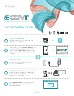
COVR-2202
Brand: D-Link Pages: 2

DAP-1155
Brand: D-Link Pages: 3

Air Premier DAP-2695
Brand: D-Link Pages: 39
AirPlus DI-714P+
Brand: D-Link Pages: 5
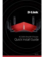
AC5300
Brand: D-Link Pages: 12
SharePort DIR-825
Brand: D-Link Pages: 20
Express EtherNetwork DI-604
Brand: D-Link Pages: 49

Xclaim Xi-2
Brand: Ruckus Wireless Pages: 3

TL-WR541G - Wireless Router
Brand: TP-Link Pages: 91

8760 - Wireless Dual Radio 11a/b/g PoE Access...
Brand: 3Com Pages: 8

Vigor 2104P
Brand: Draytek Pages: 1

Mobile WiFi Pro2
Brand: Huawei Pages: 9

Maxis Wi-Fi 6
Brand: Huawei Pages: 4

Quidway AR-28-30
Brand: Huawei Pages: 4

R216
Brand: Huawei Pages: 19

N5368X
Brand: Huawei Pages: 5


