background image

— 1 —

D825TM

SPECIFICATIONS

Picture tube

Video image area

Logical resolution

Physical resolution

Standard image area

Input signal

Video

Sync

0.25 mm aperture grill pitch
15 inches measured diagonally
90-degree deflection

(14" maximum viewing image)
Approx. 286.5 x 214 mm (w/h)
(11

3/8

 x 8

1/2 

 inches)

Horizontal: Max. 1280 dots
Vertical: Max. 1024 lines

Horizontal: Max. 1024 dots
Vertical: Max. 768 lines

Approx. 270 x 202 mm (w/h)
(10

3/4

 x 8 inches)

Analog RGB (75 ohms typical)
0.7 Vp-p, Positive
External HD/VD, Composite
Polarity Free TTL
Video Composite (Sync on Green)

0.3 Vp-p, Negative

Power Consumption

Maximum
Nominal

Deflection frequency

AC input voltage / current

Dimensions

Mass

110W
80W, 273 BTU/h

Horizontal: 30 to 70 KHz
Vertical: 50 to120 Hz

100 to 120 V, 50/60 Hz, 1.8 A
220 to 240V, 50/60Hz, 1A

368 x 392 x 384.5 mm (w/h/d)
(14

1/2

 x 15

1/2

 x 15

1/4

 inches)

Approx. 14.0 kg (30 lb 14 oz)

SERVICE MANUAL

Design and specifications are subject to change without notice.
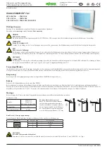
D825TM

 COLOR  MONITOR

D825TM

N. Hemisphere Model

Equator Model

Chassis No. SCC-L06C-A

R

D-1

CHASSIS

Summary of Contents for D825TM

Page 1: ... x 8 inches Analog RGB 75 ohms typical 0 7 Vp p Positive External HD VD Composite Polarity Free TTL Video Composite Sync on Green 0 3 Vp p Negative Power Consumption Maximum Nominal Deflection frequency AC input voltage current Dimensions Mass 110W 80W 273 BTU h Horizontal 30 to 70 KHz Vertical 50 to120 Hz 100 to 120 V 50 60 Hz 1 8 A 220 to 240V 50 60Hz 1A 368 x 392 x 384 5 mm w h d 141 2 x 151 2 ...

Page 2: ...13 003 10 836 11 852 µsec VERTICAL Ver Freq Hz 59 940 70 084 75 000 85 008 60 317 75 000 85 061 75 029 84 997 60 020 V Total 525 449 500 509 628 625 631 800 808 1066 V Blanking 45 49 20 29 28 25 31 32 40 42 V Front Porch 10 13 1 1 1 1 1 1 1 1 V Sync 2 2 3 3 4 3 3 3 3 3 V Back Porch 33 34 16 25 23 21 27 28 36 38 V Active 480 400 480 480 600 600 600 768 768 1024 lines SYNC Int G NO NO NO NO NO NO NO...

Page 3: ...T IDENTIFIES DANS LE PRESENT MANUEL SUIVRE CES PROCEDURES LORS DE CHAQUE REMPLACEMENT DE COMPOSANTS CRITIQUES OU LORSQU UN MAUVAIS FONTIONNEMENT SUSPECTE 1 Check the area of your repair for unsoldered or poorly soldered connections Check the entire board surface for solder splashes and bridges 2 Check the interboard wiring to ensure that no wires are pinched or contact high wattage resistors 3 Che...

Page 4: ...emoval 11 3 SAFETY RELATED ADJUSTMENT 12 4 ADJUSTMENTS 13 5 DIAGRAMS 5 1 Block Diagram 15 5 2 Circuit Boards Location 18 5 3 Schematic Diagrams and Printed Wiring Boards 18 1 D Board Schematic Diagram 19 2 A Board Schematic Diagram 23 3 D1 Board Schematic Diagram 26 5 4 Semiconductors 27 6 EXPLODED VIEWS 6 1 Chassis 29 6 2 Packing Materials 30 7 ELECTRICAL PARTS LIST 31 ...

Page 5: ...isplay Identification Data to the data line When a DDC2B host system is connected the monitor automatically switches to the appropriate standard DDCTM is a trademark of Video Electronics Standard Association Your monitor operates according to DDC2B Only computers that support the same guidelines and operate at the same or higher level can make use of this feature If your computer does not support ...

Page 6: ...ls 1 Press the MENU button to display the MENU OSD 2 Highlight the COLOR OSD using the BRIGHTNESS and CONTRAST buttons and press the MENU button again 3 Press the BRIGHTNESS buttons to select either the 9300K 5000K or variable option The 9300K and 5000K options display accurate preset color temperatures The variable option allows you to adjust the monitor using the full range of color temperatures...

Page 7: ...r press it twice to return to normal viewing Note You can enlarge or reduce the picture size until either the horizontal or vertical size reaches its maximum or minimum value 7 Using the LANGUAGE OSD You can set the OSD language to English German French Spanish or Japanese using the LANGUAGE OSD To reset to English press the RESET button while the LANGUAGE OSD is displayed 1 Press the MENU button ...

Page 8: ... is in the ON position Try pressing any key on the computer keyboard Make sure your computer is turned on Make sure the video signal cable is properly connected and all plugs are firmly seated in their sockets Make sure none of the HD15 video input connector pins are bent or pushed in Make sure the video board is completely seated in the proper bus slot Make sure the video frequency range is withi...

Page 9: ...EEN OSD page 7 If the moire is cancelled the picture may become fuzzy Decrease the moire cancellation effect using the SCREEN OSD page 7 Isolate and eliminate any potential sources of electric or magnetic fields Common causes for this symptom are electric fans fluorescent lighting and laser printers If you have another monitor close to this monitor increase the distance between them to reduce the ...

Page 10: ...L 2 2 SERVICE POSITION SECTION 2 DISASSEMBLY 1 2 3 A board D board Cabinet 1 3 2 Two screws BVTP 4 x 16 Two claws PUSH PUSH Cable bracket Cable stopper Five screws BVTP 3 x 12 D board One screw BVTT 4 x 8 1 4 5 7 3 8 A board Two screws BVTP 3 x 12 6 D1 board 2 ...

Page 11: ... CRT shield or carbon painted on the CRT after removing the anode REMOVAL PROCEDURES Do not use sharp objects which may cause damage to the surface of the anode cap Do not squeeze the rubber covering too hard to avoid damaging the anode cap A material fitting called a shatter hook terminal is built into the rubber Do not force turn the foot of the rubber cover This may cause the shatter hook termi...

Page 12: ...wn below Standard voltage 144 3 0 VDC SECTION 3 SAFETY RELATED ADJUSTMENT Part Replaced RV501 Part Replaced D BOARD When replacing parts shown in the table below the following operational checks must be performed as a safety precaution against X ray emissions from the unit Allow the unit to warm up for one minute prior to checking the following conditions a HV Regulator Check 1 Input white cross h...

Page 13: ...ion of CRT neck 5 Attach a landing adjuster sensor on the CRT 6 Using a landing checker adjust the DY position purity tilt of DY 7 Clamp the DY screw Clamping torque 22 2 kgcm 2 2 0 2 N m Convergence Rough Adjustment 1 All digital convergence data should be zero by MCP 2 Enter the white crosshatch signal 3 Adjust roughly the horizontal and vertical convergence at four pole magnet 4 Adjust roughly ...

Page 14: ... LT CBH LT Adjust each misconvergence point in sequence H STAT 11 Digital Convergence Adjustment A Horizontal Convergence 2 7 0 4 6 1 5 3 9 8 12 11 V STAT B V STAT T CCV RT MCV RT XBV R MCV RB CCV RB CCV LB MCV LB XBV L MCV LT CCV LT Adjust each misconvergence point in sequence V STAT 8 Adjust V TILT with TLV VR TLV movement 9 Adjust Y CROSS with YCH VR YCH movement 10 Paint lock the four pole and...

Page 15: ... adjustable resistors have characteristic curve B unless otherwise noted When replacing parts shown in the table below be sure to perform the safety related adjustment Part Replaced RV501 Part Replaced All voltages are in volts Readings are taken with a 10 ΜΩ digital multimeter Readings are taken with a color bar signal input Voltage variations may be noted due to normal production tolerances Cann...

Page 16: ... 26 20 28 30 DEF CONTROL IC902 28 26 17 Q903 Q501 Q502 Q511 8P CN701 CY4 CY4 CY3 CY3 CY2 CY2 CY1 CY1 IC702 CONV AMP 7 49 53 S0 S4 24 144V 15V 6 6 7 12V 5V 3 IC502 V IN H IN 46 DDCSCL DDCSDA RESET IC904 V DRIVE 5 2 H OUT V DEF 12 Q505 Q504 Q512 Q513 Q515 CONV CONTROL IC701 4 33 PCI Q521 BUFFER 18 PB1 7P HSYNC VSOUT CSYNC BPCLP SHRP1 CBLK NC HOSTGND IICSCL GND IICSDA 3 1 IC006 19 10 6 B IN G IN R IN...

Page 17: ...1 2W RC 75 RN CP 10k CHIP 4 7k CHIP 4 7k CHIP 1M CHIP 100 1 2W RC 75 RN CP 10k CHIP 4 7k CHIP 4 7k CHIP 1M CHIP 100 1 2W RC 0 1 25V B CHIP 0 1 25V B CHIP 0 1 25V B CHIP 0 1 25V B CHIP 0 1 25V B CHIP 0 1 25V B CHIP 0 1 25V B CHIP 0 1 25V B CHIP 0 1 25V B CHIP 2 2M 1W RN 0 1 25V B CHIP 0 1 25V B CHIP 220k 220k 220k 100k CHIP 10k CHIP 56k CHIP 0 01 B CHIP 2 2k CHIP 470k CHIP 0 1 25V B CHIP 0 1 25V B ...

Page 18: ...0 7 Vp p H 2 3 4 5 6 7 8 9 1 45 0 Vpk pk 45 0 Vp p H 4 5 Vp p H 4 4 Vp p H 0 7 Vp p H 45 0 Vp p H 0 7 Vp p H 4 3 Vp p H 12 11 10 ...

Page 19: ...FPRD 330 1W RS 1 8 1 2W RN 5 6k RM 2 2 1 2W RN 4 7k 47k CHIP 12k RN 0 47 FPRD 100 180k CHIP 6 8k CHIP 0 47 FPRD 10k CHIP 470k RN 1 8k RN 100 22k 22k CHIP 1 FPRD 4 7 220 2W RS 22k CHIP 22 FPRD 1k FPRD 47 47k CHIP 47k CHIP 1k FPRD 4 7k 10k 22k 10k FPRD 82 3W RS 82 3W RS 2 2 FPRD 1k FPRD 100 FPRD 47k CHIP 10 3W RS 10 3W RS 200k RN 1k RN 1k RN 4 7 FPRD 1M RN 33k RN 560k RN 82k RN 1 8k RN 33k RN 56k RN...

Page 20: ...p H 2 3 4 5 6 7 8 9 10 13 12 11 14 1 11 6 Vp p H 51 9 Vpk pk 1 3 Vp p H 5 3 Vp p H 58 1 Vp p H 5 1 Vp p V 12 3 Vp p H 3 8 Vp p 24MHZ 8 8 Vp p H 8 7 Vp p H 3 5 4 0 Vp p H 15 1 14 KVp p H 0 9 Vp p V 10 9 Vp p H ...

Page 21: ...MIZ M36LDJ15X 7 4 045 123 01 HOLDER DEGAUSSING COIL 8 4 040 897 01 SPACER DY 9 4 365 808 01 SCREW 5 TAPPING 11 1 452 923 11 NECK ASSY 12 8 451 491 11 DY Y15FRF4 M 13 1 500 386 11 FILTER CLAMP FERRITE CORE 14 A 1294 026 A A BOARD COMPLETE 15 4 050 329 01 CUSHION A 16 4 369 318 00 SPRING TENSION 17 1 409 799 11 COIL DEMAGNETIZATION 18 4 062 875 01 CABINET 19 A 1346 704 A D BOARD COMPLETE 21 1 453 25...

Page 22: ...CRIPTION REMARK D825TM 51 3 861 616 21 MANUAL INSTRUCTION 52 4 062 856 01 CUSHION UPPER 54 4 041 927 11 BAG POLYETHYLENE 55 4 062 857 01 CUSHION LOWER 56 4 062 858 01 INDIVIDUAL CARTON 6 2 PACKING MATERIALS REF NO PART NO DESCRIPTION REMARK 53 54 56 55 51 52 ...

Page 23: ...1309A 2C3311A DTC143ES DTC114EA 2SC3209 LK 16 30 1 15 9 1 CXA8070A CATHODE ANODE CATHODE ANODE K392 910 MARKING SIDE VIEW 12 n 15 1 LA7840 TDA6103Q EGP30D 2SA1162 G SB340L 6489 CATHODE ANODE 5 1234 6789 1 2 3 4 5 6 7 8 9 E B C SPB 26 CATHODE ANODE GRN ANODE RED S D G IRFU110 PST600D T Vcc GND OUT LM2405T B C E B C E 1 14 1 11 2SB1094F 2SB1375 BU2522AX G D S 2K2101 MR IRL1530GLF G S D M0C8105TV 1 2...

Page 24: ...232 11 CERAMIC CHIP 0 01MF 10 50V C028 1 104 664 11 ELECT 47MF 20 25V C029 1 164 004 11 CERAMIC CHIP 0 1MF 10 25V C035 1 162 134 11 CERAMIC 470PF 10 2KV C042 1 164 004 11 CERAMIC CHIP 0 1MF 10 25V C044 1 164 344 11 CERAMIC CHIP 0 068MF 10 25V C046 1 164 232 11 CERAMIC CHIP 0 01MF 10 50V C047 1 104 664 11 ELECT 47MF 20 25V C048 1 164 232 11 CERAMIC CHIP 0 01MF 10 50V C049 1 164 232 11 CERAMIC CHIP ...

Page 25: ...8 65 IC CXD8688P IC004 8 759 434 40 IC TDA6103Q N3 112 IC005 8 759 100 96 IC UPC4558G2 IC006 8 752 082 65 IC CXA2093S JACK J001 1 251 637 11 SOCKET CRT COIL L002 1 410 682 31 INDUCTOR 470UH L101 1 410 750 41 INDUCTOR 0 47UH L201 1 410 750 41 INDUCTOR 0 47UH L301 1 410 750 41 INDUCTOR 0 47UH TRANSISTOR Q001 8 729 032 61 TRANSISTOR 2SC5022 02 Q004 8 729 120 28 TRANSISTOR 2SC1623 L5L6 RESISTOR R002 1...

Page 26: ...073 00 RES CHIP 10K 5 1 10W R307 1 216 065 91 RES CHIP 4 7K 5 1 10W R308 1 216 065 91 RES CHIP 4 7K 5 1 10W R309 1 216 121 91 RES CHIP 1M 5 1 10W R310 1 215 477 00 METAL 220K 1 1 4W R311 1 249 401 11 CARBON 47 5 1 4W F R312 1 216 037 00 RES CHIP 330 5 1 10W R333 1 249 411 11 CARBON 330 5 1 4W R351 1 202 549 00 SOLID 100 20 1 2W SPARK GAP SG001 1 519 422 11 GAP SPARK SG101 1 517 499 21 GAP SPARK SG...

Page 27: ...M 0 36MF 5 250V C532 1 137 426 11 FILM 0 47MF 10 100V C535 1 137 370 11 FILM 0 01MF 5 50V C536 1 164 232 11 CERAMIC CHIP 0 01MF 10 50V C539 1 137 418 11 FILM 0 022MF 10 100V C540 1 136 203 11 FILM 10000PF 5 630V C541 1 126 963 11 ELECT 4 7MF 20 50V C542 1 126 964 11 ELECT 10MF 20 50V C543 1 102 973 00 CERAMIC 100PF 5 50V C544 1 137 370 11 FILM 0 01MF 5 50V C545 1 163 037 11 CERAMIC CHIP 0 022MF 10...

Page 28: ...ILM 0 068MF 5 50V C906 1 136 177 00 FILM 1MF 5 50V C908 1 164 232 11 CERAMIC CHIP 0 01MF 10 50V C909 1 126 927 11 ELECT 2200MF 20 10V C910 1 137 399 11 FILM 0 1MF 5 50V C911 1 137 370 11 FILM 0 01MF 5 50V C912 1 126 933 11 ELECT 100MF 20 16V C913 1 137 399 11 FILM 0 1MF 5 50V C914 1 102 514 11 CERAMIC 22PF 5 50V C915 1 102 514 11 CERAMIC 22PF 5 50V C916 1 126 965 11 ELECT 22MF 20 50V C917 1 163 01...

Page 29: ... 2ESB2 D624 8 719 911 19 DIODE 1SS119 25 D648 8 719 110 36 DIODE RD13ESB2 D649 8 719 991 33 DIODE 1SS133T 77 D654 8 719 109 60 DIODE RD2 7ESB2 D704 8 719 911 19 DIODE 1SS119 25 D901 8 719 911 19 DIODE 1SS119 25 D902 8 719 109 89 DIODE RD5 6ESB2 D905 8 719 911 19 DIODE 1SS119 25 D906 8 719 911 19 DIODE 1SS119 25 D907 8 719 911 19 DIODE 1SS119 25 D908 8 719 911 19 DIODE 1SS119 25 D909 8 719 109 89 D...

Page 30: ... 91 SHORT JR018 1 216 296 91 SHORT JR019 1 216 296 91 SHORT JR020 1 216 296 91 SHORT JR021 1 216 296 91 SHORT JR022 1 216 296 91 SHORT JR023 1 216 296 91 SHORT JR024 1 216 296 91 SHORT JR025 1 216 296 91 SHORT JR026 1 216 296 91 SHORT JR027 1 216 296 91 SHORT JR030 1 216 295 91 SHORT COIL L501 1 412 531 31 INDUCTOR 33UH L502 1 412 531 31 INDUCTOR 33UH L503 1 411 594 11 INDUCTOR L506 1 412 550 11 I...

Page 31: ...W F R521 1 249 417 11 CARBON 1K 5 1 4W F R522 1 249 401 11 CARBON 47 5 1 4W R523 1 216 089 91 RES CHIP 47K 5 1 10W R524 1 216 089 91 RES CHIP 47K 5 1 10W R525 1 249 417 11 CARBON 1K 5 1 4W F R526 1 249 425 11 CARBON 4 7K 5 1 4W R527 1 249 429 11 CARBON 10K 5 1 4W R528 1 247 863 91 CARBON 22K 5 1 4W R529 1 249 429 11 CARBON 10K 5 1 4W F R530 1 216 474 11 METAL OXIDE 82 5 3W F R531 1 216 474 11 META...

Page 32: ... 1 249 431 11 CARBON 15K 5 1 4W R635 1 216 049 91 RES CHIP 1K 5 1 10W R636 1 216 049 91 RES CHIP 1K 5 1 10W R637 1 216 347 11 METAL OXIDE 0 68 5 1W F R638 1 215 441 00 METAL 6 8K 1 1 4W R639 1 211 874 11 FUSIBLE 0 12 10 1 2W R641 1 249 429 11 CARBON 10K 5 1 4W F R643 1 215 435 00 METAL 3 9K 1 1 4W R649 1 218 642 11 METAL OXIDE 100K 5 1W F R703 1 260 092 11 CARBON 270 5 1 2W R704 1 215 445 00 METAL...

Page 33: ...LE RESISTOR RV501 1 241 767 21 RES ADJ CERMET 100K 3 710 578 01 COVER VOLUME 6 MOLD FOR RV501 RELAY RY601 1 755 031 11 RELAY SWITCH S601 1 571 433 21 SWITCH PUSH AC POWER S901 1 692 431 21 SWITCH TACTILE S902 1 762 816 11 SWITCH TACTILE S903 1 692 431 21 SWITCH TACTILE S904 1 692 431 21 SWITCH TACTILE S905 1 692 431 21 SWITCH TACTILE S906 1 692 431 21 SWITCH TACTILE S909 1 692 431 21 SWITCH TACTIL...

Reviews: