background image

CY24272

Rambus

®

 XDR™ Clock Generator with

Zero SDA Hold Time

Cypress Semiconductor Corporation

198 Champion Court

San Jose

,

CA 95134-1709

408-943-2600

Document Number: 001-42414 Rev. **

 Revised November 9, 2007

Features

Meets Rambus

®

 Extended Data Rate (XDR™) clocking 

requirements 

25 ps typical cycle-to-cycle jitter

–135 dBc/Hz typical phase noise at 20 MHz offset

100 or 133 MHz differential clock input

300–667 MHz high speed clock support

Quad (open drain) differential output drivers

Supports frequency multipliers: 3, 4, 5, 6, 9/2 and 15/4

Spread Aware™

2.5V operation

28-pin TSSOP package

Table 1.  Device Comparison

CY24271

CY24272

SDA hold time = 300 ns
(SMBus compliant)

SDA hold time = 0 ns
(I

2

C compliant)

R

RC

 = 200

Ω

 typical

(Rambus standard drive)

R

RC

 = 295

Ω

 minimum

(Reduced output drive)
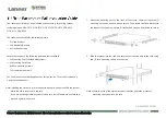
CLK0

CLK0B

CLK1

CLK1B

CLK2

CLK2B

CLK3

CLK3B

REFCLK,REFCLKB

SCL

SDA

ID0

ID1

EN

RegA

EN

RegB

EN

RegC

EN

RegD

PLL

Bypass
MUX

/BYPASS

EN

Logic Block Diagram

[+] Feedback 

Summary of Contents for Rambus XDR CY24271

Page 1: ...3 MHz differential clock input 300 667 MHz high speed clock support Quad open drain differential output drivers Supports frequency multipliers 3 4 5 6 9 2 and 15 4 Spread Aware 2 5V operation 28 pin TSSOP package Table 1 Device Comparison CY24271 CY24272 SDA hold time 300 ns SMBus compliant SDA hold time 0 ns I2 C compliant RRC 200Ω typical Rambus standard drive RRC 295Ω minimum Reduced output dri...

Page 2: ... I Device ID CMOS signal 13 ID1 I Device ID CMOS signal 14 BYPASS I REFCLK bypassing PLL CMOS signal 15 VDD PWR Power supply for outputs 16 CLK3B O Complement clock output 17 CLK3 O Clock output 18 VSS GND Ground 19 CLK2B O Complement clock output 20 CLK2 O Clock output 21 VSS GND Ground 22 VDD PWR Power supply for outputs 23 CLK1B O Complement clock output 24 CLK1 O Clock output 25 VSS GND Ground...

Page 3: ...and RegD Table 5 on page 4 shows selection from one to all four of the outputs the Outputs Disabled Mode EN low and Bypass Mode EN high BYPASS low There is an option reserved for vendor test Disabled outputs are set to High Z At power up the SMBus registers default to the last entry in Table 6 on page 5 The value at RegTest is 0 The values at RegA RegB RegC and RegD are all 1 Thus all outputs are ...

Page 4: ...ice and the lower three bits are the ID numbers assigned to the vendor by Rambus Notes 3 Bypass Mode REFCLK bypasses the PLL to the output drivers 4 Default mode of operation is at power up Table 5 Modes of Operation for CY24272 EN BYPASS RegTest RegA RegB RegC RegD CLK0 CLK0B CLK1 CLK1B CLK2 CLK2B CLK3 CLK3B L X X X X X X High Z High Z High Z High Z H X 1 X X X X Reserved for Vendor Test H L 0 X ...

Page 5: ...put Select 0 RegD 1 RW Clock 3 Output Select Table 7 Command Code 81h 5 Bit Register POD Type Description 7 Reserved 0 RW Reserved no internal function 6 Reserved 0 RW 5 Reserved 0 RW 4 Reserved 0 RW 3 Reserved 1 RW Reserved must be set to 1 for proper operation 2 REFSEL 0 RW Reference Frequency Select reference Table 3 on page 3 1 Reserved 0 RW Reserved must be set to 0 for proper operation 0 Reg...

Page 6: ...VSS 0 5 4 6 V Input Voltage REFCLK REFCLKB Relative to VSS 0 5 VDD 1 0 V Input Voltage Relative to VSS 0 5 VDD 0 5 V TS Temperature Storage Non functional 65 150 C TA Temperature Operating Ambient Functional 0 70 C TJ Temperature Junction Functional 150 C ØJA Junction to Ambient thermal resis tance Zero air flow 100 C W ESDHBM ESD Protection Human Body Model MIL STD 883 Method 3015 2000 V REFCLKB ...

Page 7: ...25 V VIL Input Signal Low Voltage at ID0 ID1 EN and BYPASS 0 15 0 8 V VIH SM Input Signal High Voltage at SCL and SDA 7 1 4 3 465 V VIL SM Input Signal Low Voltage at SCL and SDA 0 15 0 8 V VTH 8 Input Threshold Voltage for single ended REFCLK 0 35 0 5VDD V VIH SE Input Signal High Voltage for single ended REFCLK VTH 0 3 2 625 V VIL SE Input Signal Low Voltage for single ended REFCLK 0 15 VTH 0 3 ...

Page 8: ...urrent at 2 625V fref 100 MHz and fout 300 MHz 85 mA IDD 7 Power Supply Current at 2 625V fref 133 MHz and fout 667 MHz 125 mA IOL IREF Ratio of output low current to reference current 16 6 8 7 0 7 2 IOL ABS Minimum current at VOL ABS 17 25 mA VOL SDA SDA output low voltage at test condition of SDA output low current 4 mA 0 4 V IOL SDA SDA output low voltage at test condition of SDA voltage 0 8V 6...

Page 9: ... SCC PLL output phase error when tracking SSC 100 100 ps tCR tCF Output rise and fall times at 400 667 MHz measured at 20 80 of output voltage 150 ps tCR CF Difference between output rise and fall times on the same pin of the single device 20 80 of 400 667 MHz 22 100 ps Table 9 SMBus Timing Specification Parameter Description Min Max Units FSMB SMBus Operating Frequency 10 100 kHz TBUF Bus free ti...

Page 10: ...es Equal require ments apply rising edges of the CLK signal Figure 7 on page 11 shows the definition of cycle to cycle duty cycle error tDC ERR Cycle to cycle duty cycle is defined as the difference between tPW high times of adjacent differential clock cycles Equal requirements apply to tPW low times of the differential click cycles Differential Driver CLK CLKB Swing Current Control ISET RRC Measu...

Page 11: ...Voltage Figure 6 Cycle to cycle Jitter Figure 7 Cycle to cycle Duty cycle Error VH tR tF 80 20 VL V t Vx nom CLK CLKB Vx Vx CLK CLKB tCYCLE i tCYCLE i 1 tJ tCYCLE i tCYCLE i 1 over 10 000 consecutive cycles CLK CLKB tCYCLE i tPW i tPW i tPW i 1 tPW i 1 tCYCLE i 1 tDC ERR tPW i tPW i 1 and tPW i 1 tPW i 1 Feedback ...

Page 12: ...b Free CY24272ZXC 28 pin TSSOP Commercial 0 C to 70 C CY24272ZXCT 28 pin TSSOP Tape and Reel Commercial 0 C to 70 C PIN 1 ID SEATING PLANE BSC BSC 0 8 PLANE GAUGE 1 28 9 60 0 378 1 10 0 043 MAX 0 65 0 025 0 20 0 008 0 05 0 002 6 50 0 256 0 076 0 003 6 25 0 246 4 50 0 177 4 30 0 169 9 80 0 386 0 15 0 006 0 19 0 007 0 30 0 012 0 09 0 003 0 25 0 010 0 70 0 027 0 50 0 020 0 95 0 037 0 85 0 033 51 8512...

Page 13: ...r firmware is owned by Cypress Semiconductor Corporation Cypress and is protected by and subject to worldwide patent protection United States and foreign United States copyright laws and international treaty provisions Cypress hereby grants to licensee a personal non exclusive non transferable license to copy use modify create derivative works of and compile the Cypress Source Code and derivative ...

Reviews: