background image


CDB43198-GBK 


CDB43198-GBK Kit Manual 


http://www.cirrus.com 

Copyright ©


2018 Cirrus Logic, Inc. and 

Cirrus Logic International Semiconductor Ltd. 

All rights reserved. 

DS1156DB1


AUG '18


Features


  Configurable serial audio headers for PCM, DSD and DoP audio 

  Headphone and line outputs 

  Analog and S/PDIF audio input 

  USB audio module capability 


WISCE™ I

2

C-based software control 

  Windows® compatible 

Description


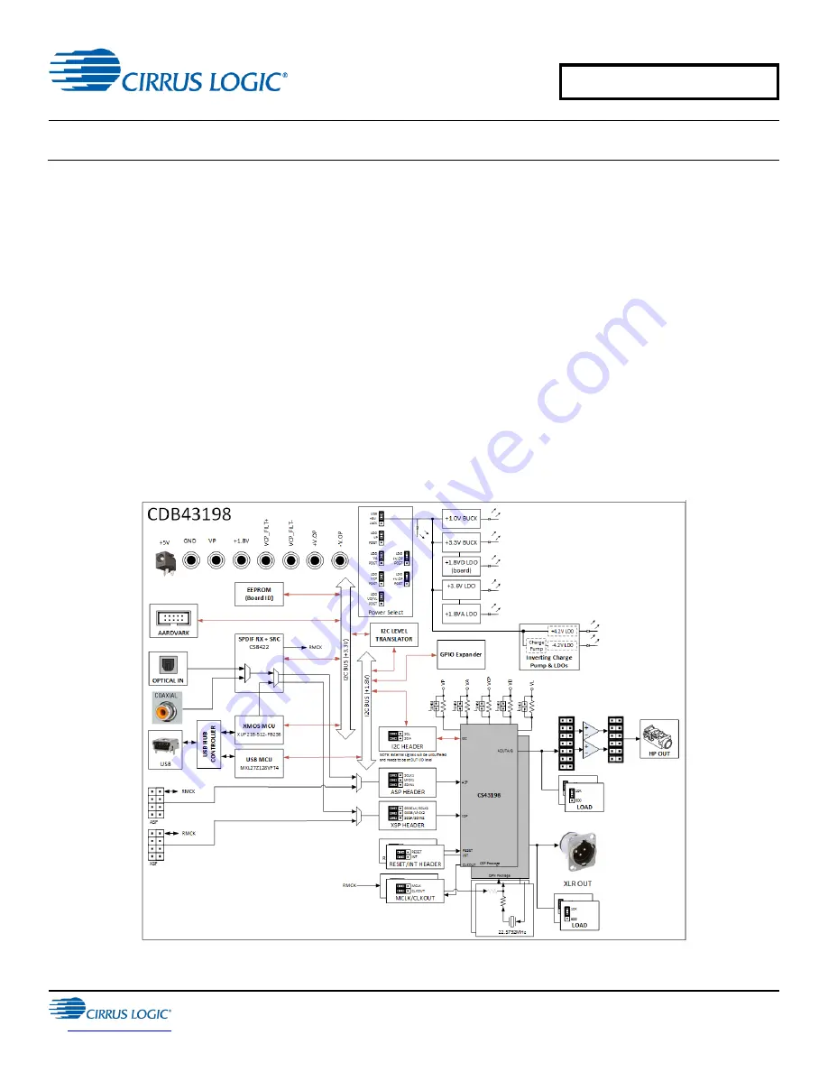
The CDB43198-GBK is a dedicated platform for testing and evaluating the CS43198. The CS43198 is a high-performance 
audio DAC with integrated impedance detection and headphone drivers. To allow comprehensive testing and evaluation 
of the performance of the CS43198, extensive software-configurable options are available through the CDB43198 
evaluation kit. The kit also included the CDB-HDR-MEAS, for measuring the 130 dB dynamic range performance of the 
CS43198. 

Software options, such as register settings for the CS43198, are configured via the WISCE software tool, which 
communicates with the CDB43198-GBK via an Aardvark I

2

C/SPI host adapter from a Windows computer, or via Mini-USB 

cable. 


Figure 1  CDB43198 Board Block Diagram 


Summary of Contents for CDB43198-GBK

Page 1: ...ting the CS43198 The CS43198 is a high performance audio DAC with integrated impedance detection and headphone drivers To allow comprehensive testing and evaluation of the performance of the CS43198 extensive software configurable options are available through the CDB43198 evaluation kit The kit also included the CDB HDR MEAS for measuring the 130 dB dynamic range performance of the CS43198 Softwa...

Page 2: ...ter Quick Reference 17 3 1 Register Descriptions 17 4 CDB HDR MEAS High Dynamic Range Measurement Preamplifier 21 4 1 Powering the CDB HDR MEAS 21 4 2 How the CDB HDR MEAS Works 22 5 Testing the CS43198 using WISCE 23 5 1 Launching WISCE 23 5 2 Loading the CDB43198 board Panel and Register Map 24 5 3 Loading the CS43198 Plugins and Register Map 26 5 4 Initializing the Devices on the CDB43198 Board...

Page 3: ...98 GBK kit consists of an evaluation board a high dynamic range HDR measurement board and a USB cable Each of these component boards is described in the following sections 1 1 CDB43198 Board The CDB43198 is shown in the following figure Figure 2 CDB43198 Base Board ...

Page 4: ...1 1 2 CDB HDR MEAS Board The CDB HDR MEAS is shown in the following figure This board is used for measuring the very low HDR of the device with an Audio Precision SYS 2700 or APx555 audio analyzer Figure 3 CDB HDR MEAS Board ...

Page 5: ...ough its I2 C interface The register map for I O Expander is described in Section 3 The direction of clock signals is determined by the CS43198 s operating mode master or slave mode The CDB43198 can also communicate with a smart codec through the use of J42 The purpose of using a smart codec is to allow the user to perform listening tests with various equalizer EQ filters based on the impedance of...

Page 6: ... bench supplies via banana jacks The switchers and LDOs step down the 5 V supply to 3 6 V 3 3 V 1 0 V 1 8 V analog and 1 8 V digital levels If the device is set into External VCP_FILT Supply Mode and bypass the internal Class H charge pump circuit then a 3 volt supply must be applied to VCP_FILT and VCP_FILT The banana jacks are connected to each device through a set of resistors R24 R25 for the C...

Page 7: ...re routed to from the CS43198 using voltage level translation buffers The direction of clock and data through these buffers is controlled using on board TCA6424 I O Expander IC U9 U12 and U15 translate the signals on J25 and J26 from a voltage of 3 3 V or 1 8 V to the operational voltage of 1 8 V The ASP signals are then fed into J24 while the XSP signals are fed into J44 These 3x3 pin headers are...

Page 8: ...e jumpers between the two columns of pins labeled BRD and DUT For example in order to send SCLK1 LRCLK1 and SDIN1 signals from the buffer to the DAC place jumpers between pins of the BRD and DUT group as shown in the following figure Figure 6 Jumper Settings to Route Signals from Buffers to DUT ...

Page 9: ...APx to LRCLK1 pins in the AP group and the RXDAT1 output from the APx to SDIN1 pins in the AP group as shown in the following figure Figure 7 External Audio Source to DUT 2 2 2 S PDIF Receiver The CS8422 S PDIF receiver provides two channel digital input either from an optical or coax connector The CS8422 can support sample rates up to 211 kHz and data output with either 16 18 20 or 24 bit word le...

Page 10: ...1156DB1 2 3 Analog Audio Output The CDB43198 board has one 1 8 stereo headphone output jack J1 for the CSP and one XLR cable output jack J60 for the QFN Figure 8 1 8 Headphone Jack APx Connectors Loading Jumpers for CSP ...

Page 11: ... By default the jumpers are installed horizontally Figure 9 J21 Opamp Header Table 4 J21 Header Pinout Header Pins Designation Description J42 1 2 V OP 4 2 V OP AMP Power 3 4 V OP 4 2 V OP AMP Power 5 OUTA Signal coming from OUTA of the CS43198 6 INA OP Input to OP AMP A Non Inverting 7 8 GND Ground 9 OUTB Signal coming from OUTB of the CS43198 10 INB OP Input to OP AMP B Non Inverting 11 REFA CSP...

Page 12: ...nce from HP Jack for Inverting OP AMP A Input 3 OUTA OP Output of OP AMP A 4 OUTA HP Output of OP AMP A to Channel A of Headphone Jack 5 OUTB OP Output of OP AMP B 6 OUTB HP Output of OP AMP B to Channel B of Headphone Jack 7 INB OP Input to OP AMP B Inverting 8 INB HP Reference from HP Jack for Inverting OP AMP B Input 9 REFA OP OUTA Reference passing through the OP AMP Section 10 REFA HP GND Hea...

Page 13: ...hip select 8 SPI_MOSI SPI master out slave in 2 10 GND Ground reference 4 6 NC No connect 2 6 LEDs The status LEDs on the CDB43198 board show the status of the power rails and S PDIF input A summary of the LEDs is shown in the table below Table 7 Status LEDs LED Function LED Reference LED Color Description INT_QFN D1 Orange Interrupt from QFN OFF No Interrupt 3 6VP D2 Green Presence of 3 6 V rail ...

Page 14: ... I External source for 4 2V rail for external OP AMP J15 CSP AOUTA Loading 3x1 header Selectable loading resistance of 600 10k Ω for CSP AOUTA J16 V OP Banana Jack Banana jack I External source for 4 2V rail for external OP AMP J17 QFN AOUTA Loading 3x1 header Selectable loading resistance of 600 10k Ω for QFN AOUTA J18 V OP Source Select 3x1 header Jumper between 1 2 to get V OP from 4 2 V banana...

Page 15: ...ly J52 Jumper between 2 3 to get 4 V from USB VBUS J43 J53 I2 C DUT Connection 3x2 header Connect shunt between DUT BRD to connect DUT and I2C data Disconnect shunt and use 2 pin test point for Audio Precision between DUT GND to measure I2C data directly J54 RST INT CSP Connection 3x2 header Connect shunt between DUT BRD to connect RST and INT data Disconnect shunt and use 2 pin test point for Aud...

Page 16: ... CSP CS43198 QFN 2 8 Codec MCLK Selection The MCLK input to the smart codec can come either from the on board 24 576 MHz clock oscillator a 22 579 MHz clock oscillator MCLK1 from ASP J25 MCLK2 from XSP J26 or from the CLKOUT pin on the DAC or the MCLK output from an external audio source The selection is controlled by WISCE Figure 11 CODEC MCLK Selection 2 9 Clock Sources The CDB43198 Board has 2 ...

Page 17: ...D RESER VED Default Value 1 1 1 1 X 1 X X Bits Name Description 7 XTI_OSC_24p576MHZ_EN Enable 24 576 MHz CLK to be used as input to CODEC 0 Enabled 1 Disabled Default 6 XTI_OSC_22p5792MHZ_EN Enable 22 5792 MHz CLK to be used as input to CODEC 0 Enabled 1 Disabled Default 5 XTI_CLKOUT_EN Select SPDIF Clock Master 0 External CLK 1 CS43198 CLKOUT Default 4 XTI_CLKOUT_CSP QFN Select Device to be SPDIF...

Page 18: ... DSD 1 SPDIF Default 6 ASP_PCM SPDIF Set Codec in PCM SPDIF Mode 0 PCM 1 SPDIF Default 5 XSP_M S Set XSP as Master Slave 1 Master Default 0 Slave 4 ASP_M S Set ASP as Master Slave 1 Master Default 0 Slave 3 MCLK2_HDR_M S Set Codec as Master to MCLK2 1 Master Default 0 Slave 2 MCLK1_HDR_M S Set Codec as Master to MCLK1 1 Master Default 0 Slave 1 XTI_MCLK2_BRD_EN Enable ASP MCLK to be used as input ...

Page 19: ...OU T_EN_DIR XTI_CLKOU T_CSP QFN _DIR Reserved RESET_SP DIF_DIR RESET_DU T2 RESET_DU T1 Default Value 0 0 0 0 x 0 1 1 Bits Name Description 7 XTI_OSC_24_576MHZ_EN_DIR Direction of the XTI_OSC_24_576MHz_EN signal 0 Output Default 1 Input 6 XTI_OSC_22_5792HZ_EN_DIR Direction of the XTI_OSC_24_5792MHz_EN signal 0 Output Default 1 Input 5 XTI_CLKOUT_EN_DIR Direction of the XTI_CLKOUT_EN signal 0 Output...

Page 20: ... S_DIR Direction of the ASP_M S signal 0 Output Default 1 Input 3 MCLK2_HDR_M S_DIR Direction of the MCLK2_HDR_M S signal 0 Output Default 1 Input 2 MCLK1_HDR_M S_DIR Direction of the MCLK1_HDR_M S signal 0 Output Default 1 Input 1 XTI_MCLK2_BRD_EN_DIR Direction of the XTI_MCLK2_BRD_EN signal 0 Output Default 1 Input 0 XTI_MCLK1_BRD_EN_DIR Direction of the XTI_MCLK1_BRD_EN signal 0 Output Default ...

Page 21: ... dynamic range DNR of the CS43198 The CDB HDR MEAS preserves the dynamic range of the input signal while amplifying the input signal by 13 66 dB to overcome noise floor limitations of the audio analyzer 4 1 Powering the CDB HDR MEAS The CDB HDR MEAS board requires a triple output DC power supply capable of providing 15 V and GND connection at 100 mA as shown in the figure below Standard binding po...

Page 22: ...t the difference results in a measurement error that hampers performance Figure 15 Testing Without CDB HDR MEAS To rectify this issue the input signal can be amplified in this case by 13 3 dB This will also amplify the noise floor however since the noise floor is small compared to the signal the signal will dominate the amplification In the figure below the signal and noise floor have been shifted...

Page 23: ...ol for setting up and configuring Cirrus Logic devices and software The following sections show how to use WISCE to configure and test CS43198 and using the CDB43198 board and the CDB43198 Board 5 1 Launching WISCE Click on the Start Button All Programs Wolfson Evaluation Software and select WISCE V3 to launch WISCE Figure 17 Launch WISCE ...

Page 24: ... Expander The device at address 0x60 is CS43198 CSP DUT and the device at address 0x62 is the CS43198 QFN DUT Figure 18 Found Devices 5 2 Loading the CDB43198 board Panel and Register Map To load the CDB43198 board panel and register map double click on the Unknown device at address 0x44 to launch Change Device pop up window Alternatively the Change Device pop up window can also be launched by rig...

Page 25: ...CDB43198 GBK DS1156DB1 25 Click Accept to load the CDB43198 board Panel and Register Map shown in the following figures Figure 20 TCA6424 Panel Figure 21 TCA6424 Register Map ...

Page 26: ...pop up window by either double clicking on Unknown Device or right clicking on Unknown Device at address 0x60 and selecting Properties Select CS43198 Rev A1 from the Device drop down menu and click Accept to load the plugin and register map for the CS43198 Figure 22 Select CS43198 CSP Figure 23 Select CS43198 QFN Figure 24 CS43198 Register Map ...

Page 27: ...CDB43198 GBK DS1156DB1 27 To view CS43198 plugin click on Tuning and select CS43198_Plugin Figure 25 CS43198 Plugin ...

Page 28: ...e CDB43198 Board The following steps show how to detect the presence of the CS43198s on the CDB43198 Board 1 Under the CDB431XX_I2C_GPIP_EXP menu click on QUICK_START and click CDB_INIT txt This will reset the board into a default mode Figure 26 Initialize DACs ...

Page 29: ...e each tab and its function The user can configure the CS43198 using these tabs However it is recommended that the user initially use the profile scripts that are provided with the plugin to configure and control the CS43198 since each field will be preconfigured correctly for the proper mode 5 5 1 Main Tab This tab shows the block diagram of the internal architecture of the CS43198 Figure 27 Main...

Page 30: ...98 GBK 30 DS1156DB1 5 5 2 Sys_Config Tab This tab allows user to configure the CS43198 clock input settings It also allows the user to configure CLKOUT and Class H amplifier settings Figure 28 Sys_Config Tab ...

Page 31: ...ce by clicking on the Power Down XTAL LED LED color will change to Red 4 Click on XTAL Status button If Ready LED is lit the crystal Interface has been configured successfully and the CS43198 is ready to use XTAL as MCLK source Go to step 6 5 If Error LED is lit then the crystal interface is not configured Power down the board Check the crystal and the crystal circuit on the board 6 Select XTAL fr...

Page 32: ...CDB43198 GBK 32 DS1156DB1 5 5 3 PLL Tab This tab allows the user to configure the CS43198 PLL The PLL can be used as an alternate source for the CS43198 MCLK Figure 30 PLL Tab ...

Page 33: ... 31 Headphone Tab 5 5 4 1 Enabling Headphone Output The following steps show how to enable the headphone output using the Headphone tab 1 Enable headphone interrupts by checking the Enable Headphone Interrupts check box 2 Configure MCLK source Configure audio input port 3 Power up headphone by checking the Enable Headphone Output check box 4 The headphone output should be powered up ...

Page 34: ...o indicate headphone has been powered down 5 5 4 3 Headphone Presence Detection The following steps show how to enable headphone presence detection 1 Enable headphone interrupts by checking the Enable Headphone Interrupts check box 2 Enable invert detection to account for the tip detect pin setup of the headphone jack by checking the Invert Detect check box 3 Enable headphone presence detection by...

Page 35: ...CDB43198 GBK DS1156DB1 35 Figure 32 ASP Config Tab ...

Page 36: ...CDB43198 GBK 36 DS1156DB1 The following figure shows the contents of ASP Config tab when ASP is configured to operate in Master mode Figure 33 ASP Config Tab in Master Mode ...

Page 37: ...al MCLK MCLK_INT and the values in ASP Numerator ASP Denominator LRCLK high Time and LRCLK Period text boxes The value in the LRCLK Frequency text box will be used to set the new sample rate if it is not already set by user when the ASP is powered up Figure 34 Calculating ASP Clock Frequencies It is recommended to use a profile script to configure this port since each field will be preconfigured c...

Page 38: ...S1156DB1 5 5 6 XSP Config Tab This tab allows the user to configure the XSP port The following figure shows XSP Config tab contents when XSP is configured to operate in Slave mode Figure 35 XSP Config Tab in Slave Mode ...

Page 39: ...CDB43198 GBK DS1156DB1 39 The following figure shows the contents of XSP Config tab when XSP is configured to operate in Master mode Figure 36 XSP Config Tab in Master mode ...

Page 40: ...al MCLK MCLK_INT and the values in XSP Numerator XSP Denominator LRCLK high Time and LRCLK Period text boxes The value in the LRCLK Frequency text box will be used to set the new sample rate if it is not already set by user when the XSP is powered up Figure 37 Calculating XSP Clock Frequencies It is recommended to use a profile script to configure this port since each field will be preconfigured c...

Page 41: ...This tab allows the user to change PCM filter dynamically during playback The impulse and magnitude responses of the selected filter are displayed It is recommended to use a profile script to configure this part since each field will be preconfigured correctly for the proper mode Figure 38 PCM Playback Tab ...

Page 42: ...DB43198 GBK 42 DS1156DB1 5 5 8 DSD Playback Tab This tab allows the user to configure the DSD DoP playback path It is recommended to use a profile script to configure this port Figure 39 DSD Playback Tab ...

Page 43: ...ack_xxx_yyy 2 xxx is the sample rate yyy is the output voltage level PCM through ASP header J25 DSD Playback Slave CDB_DSD_In_Ext_Slave Slave_DSD_Playback_xxx_yyy 3 xxx is the DSD Speed yyy is the output voltage level DSD through XSP header J26 DoP Playback 64fs Mode Slave CDB_PCM_In_Ext_Slave DoP_DSD64_playback_XTAL_Slave PCM through ASP header J25 CDB_Spdif_In_Clk_External DoP_DSD64_playback_XTA...

Page 44: ...CDB43198 GBK 44 DS1156DB1 6 1 Data Flow for Various Use Cases The following sections depict the flow of data in red for various common use cases 6 1 1 PCM Playback Figure 40 PCM Playback Data Flow ...

Page 45: ...CDB43198 GBK DS1156DB1 45 6 1 2 DSD Playback Figure 41 DSD Playback Data Flow ...

Page 46: ...ke sure that the CDB43198 jumpers are set to factory default mode 1 Power up the CDB43198 by applying 5 V or VBUS through a USB connection 2 Connect a cable from Digital Serial IO Transmitter port of an APx e g APx555 to header J25 on CDB43198 board There is no need to connect the MCLK signal 3 Follow the steps described in the Quick Setup Guide to launch WISCE and load plugins 4 Load the profile ...

Page 47: ...figure the APx for running the tests This procedure was tested using an APx555 1 Run the APx software APx500 v4 2 if using an APx555 2 Set the APx Output to Digital Serial and Input to Analog Balanced 3 Set the Input Bandwidth to 20 Hz to 22 4 kHz Figure 43 APx Signal Path Setup ...

Page 48: ...43198 GBK 48 DS1156DB1 4 In the Signal Path Setup panel click on the settings button next to Connector drop down menu and configure Digital Serial Settings as shown below Figure 44 Digital Serial Settings ...

Page 49: ...8 GBK DS1156DB1 49 5 To launch the Dynamic Range Measurement test click on Project Add Measurement Meters Dynamic Range AES17 This will launch the dynamic range test screen Figure 45 Launch Dynamic Range Test ...

Page 50: ... 6 To run the Dynamic Range Measurement test configure the Input Level and Bandwidth as shown below Click on the Start button to run the test Dynamic Range values will be displayed for both channels Figure 46 Dynamic Range Test ...

Page 51: ...CDB43198 GBK DS1156DB1 51 7 To launch THD N test click on Project Add Measurement Meters THD N to launch THD N measurement window Figure 47 Launch THD N Test ...

Page 52: ... shown below Click on the Generator button to run the test THD N ratio will be displayed for both channels THD N ratio is typically displayed in Percentage To display the values in dB select dB from the drop down menu next to Unit on top of the display Figure 48 THD N Measurement Settings ...

Page 53: ... HDR MEAS board 6 2 3 1 Measuring Dynamic Range The following steps show the procedure to measure dynamic range 1 Place a jumper connecting the 600 Ω load on J15 2 Place a jumper connecting the 600 Ω load on J4 3 Connect a headphone cable between CSP AOUT J1 and the input of the CDB HDR MEAS 4 Power up the CDB HDR MEAS board with 15V and GND 5 For each channel connect a cable between the BNC jacks...

Page 54: ... Slave Mode 6 2 4 1 Measuring THD N on CSP Device The following steps show the procedure to measure THD N 1 Place a jumper connecting the 600 Ω load on J15 2 Place a jumper connecting the 600 Ω load on J4 3 Connect a headphone RCA or headphone BNC cable between CSP AOUT J1 and the Balanced port on Analog inputs 1 and 2 on the APx Figure 50 THD N Measurement for CS43198 CSP 4 Configure APx and run ...

Page 55: ...N 1 Place a jumper connecting the 600 Ω load on J17 2 Place a jumper connecting the 600 Ω load on J31 3 Connect a XLR cable between QFN OUT J60 and the Balanced XLR port on Analog input 1 on the APx Figure 51 THD N Measurement for CS43198 QFN 4 Configure APx and run THD N Measurement test as described in section 6 2 2 ...

Page 56: ...le voltage conditions Table 14 Measured THD N Results Output Load R L Full Scale Voltage VRMS Channel Datasheet Spec Typical Measured Result 1 10k 1 7 A 115 dB 113 9 dB B 113 6 dB XLR 114 4 dB 600 1 7 A 115 dB 113 4 dB B 113 7 dB XLR 114 9 dB Notes 1 Refer to CS43198 data sheet for test conditions 6 3 3 Dynamic Range DNR Results The table below lists measured DNR results using the test waveforms u...

Page 57: ...LY AT THE CUSTOMER S RISK AND CIRRUS LOGIC DISCLAIMS AND MAKES NO WARRANTY EXPRESS STATUTORY OR IMPLIED INCLUDING THE IMPLIED WARRANTIES OF MERCHANTABILITY AND FITNESS FOR PARTICULAR PURPOSE WITH REGARD TO ANY CIRRUS LOGIC PRODUCT THAT IS USED IN SUCH A MANNER IF THE CUSTOMER OR CUSTOMER S CUSTOMER USES OR PERMITS THE USE OF CIRRUS LOGIC PRODUCTS IN CRITICAL APPLICATIONS CUSTOMER AGREES BY SUCH US...

Reviews: