background image

Summary of Contents for Little Board/PLUS

Page 1: ...COMPUTERS INCORPORATED LITTLE BOARD PLUS TECHNICAL MANUAL Part Number A74010 Revision B 67 EastEvelynAve MountainView CA94041 415 962 0230...

Page 2: ...ical information on Little Board PLUS hardware Chapter 5 PROGRAMMER S REFERENCE I O port addresses and programming information regarding custom programming of Little Board PLUS Only brief descriptions...

Page 3: ...3 1 Introduction 3 1 1 Software References 3 1 2 Conventions 3 2 First Time Use 3 2 1 Making Backup Disks 3 2 2 Customizing Your System Disk 3 3 Operating System Features 3 3 1 CP M 2 2 BDOS 3 3 2 AM...

Page 4: ...neration 5 S Floppy Disk Interface 5 9 Parallel Printer Port 5 10 ID Input Port 5 11 SCSI PLUS Interface 5 11 1 SCSI SASI Programming 5 11 2 Simple Bidirectional I O 5 1 5 1 5 1 5 2 5 3 5 3 5 4 5 5 5...

Page 5: ...4K bytes dynamic RAM 4K 32K EPROM Two spare counter timer channels Floppy controller capable of controlling from one to four single or doubl sided single or double density 40 or 80 track mini or micro...

Page 6: ...es two fully pro grammable serial I O ports Each channel has four of the standard RS232C signals TxD RxD RTS and CTS These signals are sufficient for interfacing most serial printers modems and termin...

Page 7: ...dis connect reselect In addition Little Board PLUS supports the Initiator function of AMPRO s innovative SCSI PLUS extension to SCSI This allows connection of up to 64 SCSI PLUS Target devices rather...

Page 8: ...be output Printer Busy input 12 Ground pins DISK I O No drives supported 1 4 Disk Controller WD1772 Data rate 250k bps MFM 125K bps FM Sector size 128 256 512 or 1024 bytes Phase locked loop digital 8...

Page 9: ...on 2 2 and BIOS on diskette Little Board Plus system utilities Option FRIENDLY Integrated Operating Environment Option BIOS and Utilities source code DOCUMENTATION Little Board Plus Technical Manual L...

Page 10: ......

Page 11: ...ble 2 1 System Components Description 1 to 4 mini or micro floppy drives 40 or 80 track single or double sided Adaptec ACB 4000 or Xebec 1410 A or equivalent SCSI SASI hard disk controller 5 to 20 Meg...

Page 12: ...rs T B 609 3415M Molex 15 29 0341 J8 SCSI PLUS Interface T B 609 5000M Molex 15 29 8502 Berg 66902 150 NOTE All Little Board PLUS s oftware is distributed on double sided 48 tpi AMPRO format mini flop...

Page 13: ...PARALLEL PRINTER J 0 POWER o SERIAL A SERIAL B RESET POWER LED FLOPPY mINPUT Figure 2 1 Little Board PLUS Connector Locations 2 3...

Page 14: ...wer LED This connector is for connection to an external SPST switch to provide the master RESET signal In addition a 15 rnA current source provides power to an LED power on indicator Refer to Table 2...

Page 15: ...rs from that of Centronics connectors even though the required inter connection cable is straight through To clarify this each signal s corres ponding Centronics connector pin number has been included...

Page 16: ...34 READY Drive ready option in 1 33 all odd pins Signal grounds Nearly any type of soft sectored single or double sided 40 or 80 track mini 5 1 4 or micro 3 to 4 floppy disk drive is usable with the...

Page 17: ...nnector to interface with SCSI compatible peripherals Table 2 8 shows the signal names and pin numbers for the SCSI PLUS bus interface connector Refer to your disk con troller documentation or the ANS...

Page 18: ...required for this purpose the ID Input Port can be used as a general purpose 8 bit input port connector with a flat ribbon cable connector plugged onto J7 Table 2 9 shows the signal names and pin numb...

Page 19: ...CLK TRG3 input JMP2 2 to either the 1772 FDC s interrupt request output signal JMP2 3 or to the CTC s ZC TC2 output signal JMP2 1 FACTORY SETTING both options open JIIP3 CTC CLK TRG2 This jumper when...

Page 20: ...the 28 pin EPROM socket so that the 2732 s pin 1 plugs into pin 3 of the socket dMP7 DART RIA This jumper when shorted connects the 1772 FDC s DRQ output singal JMP7 2 to the DART s RIA input JMP7 1...

Page 21: ...so be replaced with alternate values NOTE The on board resistive termination networks UI7 U22 should be present on two and only two SCSI bus devices Be sure that the board s SCSI bus is terminated in...

Page 22: ...on 2 5 TROUBLESHOOTING It is possible that the completed system does not work the first time If you have to troubleshoot it here are some suggestions Recheck all wiring soldered connections Check that...

Page 23: ...n the program s use Full descriptions and operating instructions for the AMPRO software utilities are found in the AMPRO Z80 System Software User s Manual AMPRO part number A74006 Some recommended CP...

Page 24: ...identical format types When making a backup in which the source and destination disks will be the same floppy format i e 48 to 48 tpi or 96 to 96 tpi the backup can easily be made with the Copy funct...

Page 25: ...ly not perfect for your system configuration The AMPRO CONFIG utility allows you to easily modify the serial port setups baud rates handshaking etc printer port assignment serial or parallel floppy dr...

Page 26: ...ons Many features of the Little Board PLUS CP M operating system are the result of a highly flexible sophisticated BIOS implementation Here are a few Automatic Format Sensing Single and double sided 4...

Page 27: ...CP M console command processor CCP has been replaced with the more powerful Z80 Command Processor Replacement version 3 ZCPR3 As indi cated in Table 3 2 the ZCPR3 implementation differs slightly from...

Page 28: ...er number e g AO B15 C 13 ufn Unambiguous file name e g MYFILE TXT DIR COM afn Ambiguous file name e g COM MYFILE M ILE T T Sub Directories Each floppy disk has a directory of files each directory can...

Page 29: ...few nice features such as alphabetical file sorting and direct access to any directory For example AO DIR B5 RETURN displays the directory of drive B user area 5 sorted alphabetically Also since the d...

Page 30: ...dard CP M version 2 2 intrinsic commands are implemented as well as some additions Table 3 2 lists the ZCPR3 commands versus those of the standard CP M CCP Aliases One of the most powerful features of...

Page 31: ...ard PLUS This section contains brief descriptions of each They include the standard CP M 2 2 software set the AMPRO Little Board PLUS utilities several key ZCPR3 utilities several public domain progra...

Page 32: ...istics and hand shaking floppy drive step rates printer port choice serial or parallel and command for power up or reset automatic execution DOS COII Used to read and write files on MS DOS format disk...

Page 33: ...The following ZCPR3 utilities are included on the Little Board PLUS system disk Source code is available from ECHELON Inc 415 948 3820 at nominal cost ALIAS COII Used to create or modify multiple comm...

Page 34: ...rogram Modified for use with the Little Board PLUS serial port B AMPRO specific overlay is contained in the file M LB ASM Allows direct computer to computer file transfer over Rs232 or may be used wit...

Page 35: ...in less memory required for the operating system allowing the operating system bo be moved up in memory In the fifth case sligntly more program area is made available by using a BIOS with a few less...

Page 36: ......

Page 37: ...AM t t RESET INTERNAL BUS t 5V FLOPPY DUAL PARALLEL SCSI PLUSTII l PRINTER BUS yyy CONTROLLER UART 330n PORT INTERFACE v34 6 I 6 26 50 PORTA PORTB 1 4 TERMINALS CENTRONICS 1 0 EXPANSION BUS FLOPPY MOD...

Page 38: ...selects the EPROM rather than RAM In addition a wait state generator becomes active whenever the EPROM is selected permitting the use of EPROM device access times up to 450 nS A programmable array log...

Page 39: ...are not unabiguously decoded Refer to Table 4 1 4 3 BOARD CONTROL REGISTER The Board Control Register BCR is a simple octal output latch which controls several board functions Seven of the eight bits...

Page 40: ...rallel printer port data lines In addition there are two handshaking signals Data Strobe output and Busy input The Data Strobe output is generated by a flip flop which is set and reset by software Thi...

Page 41: ...ohm termination networks provide optional on board SCSI bus termination The 5380 is fully compatible with the ANSC X3T9 2 SCSI standard including all roles and all phases In addition the 5380 can sup...

Page 42: ......

Page 43: ...rity daisy chain is fully implemented with the following prioritization The CTC device has the highest interrupt priority with each channel sub prioritized channel 0 is highest channel 3 lowest DART C...

Page 44: ...itched between 8 MHz FDCHI 0 and 16 MHz FDCHI 1 This theoretically allows the 1772 to function at eight inch floppy drives when its clock is set to 16 MHz However the 1772 is currently not guaranteed...

Page 45: ...60h and 70h as shown in Table 5 2 Table 5 2 CTC Register Addresses Address CTC Channel 40H 0 50H 1 60H 2 70H 3 All Channels are read write The CTC master clock is the 4 00 MHz system clock The Clock i...

Page 46: ...available for use as general purpose interrupt sources The DART internal registers are accessed through four non consecutive I O addresses as shown in Table 5 3 Each register is both read and write N...

Page 47: ...gnment Signal Name DART Pin Function Serial Port Functions Transmit Data TXDB output to RS232C Receive Data RXDB input from RS232C Handshake Out RTSB output to RS232C Handshake Input CTSB input from R...

Page 48: ...5 6 and 5 7 For information on programming of the CTC and DART devices refer to the device data sheets Appendix D Table 5 7 lists the available baud rates through the CTC clock sources Table 5 6 Baud...

Page 49: ...required DART Scale Factor to be written to the DART To program Serial Port A for the higher baud rates Issue a software reset to CTC Channel O Write a 03H byte as a control word to CTC Channel 0 Cle...

Page 50: ...you modify the standard Little Board PLUS FDC drivers source is available from AMPRO rather than creating new custom routines 5 9 PARALLEL PRINTER PORT The parallel printer interface supports eight d...

Page 51: ...e level on the input pin When a jumper is inserted the corresponding data is low 0 when out the data bit is high 1 Jumper assignment is as follows J7 pins 1 and 2 corresponds to data bit 7 pins 3 and...

Page 52: ...details AMPRO s proposed enhancement to SCSI to allow 64 rather than 8 bus devices is available from AMPRO 5 11 1 SCSI SASI Programming When using the SCSI PLUS interface with SCSI SASI disk controll...

Page 53: ...380 is placed in Target mode by writing 40h to the Mode Register Once in Target mode all 17 I O signals except ACK and ATN may be used as both inputs and outputs In Target mode ACK and ATN are inputs...

Page 54: ......

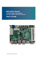
Page 55: ...APPENDIX A BOARD DIAGRAM PARTS LIST AND SCHEMTAIC A l...

Page 56: ..._ALL O _TIf L Uu eo d AeOOeO J U U UJ UI CIO Ie e I Iit j U Ii IR 0 0 1 1 1 J I 1 c B cI U il ca W c l JI 1 CIS J8 J2 _ 11 l 1 U1 f O 1 I 0 uS C1 I I n e n I J J 1 0 L m 9 0 E 4 J nJ n n u u Ig O e u...

Page 57: ...2POS 100 0C 40 MAX HEIGHT RES CF 4700 5 1 4W RES CF 1K 5 1 4W RES CF 3 3 5 1 4W RES CF 10K 5 1 4W RES PK 8SIP 7 4700 5 RES PK 8SIP 7 1K 5 RES PK 8SIP 7 330 5 OSCILLATOR 16 000MHZ IC 74F163 OR 74F161 I...

Page 58: ...IC 74LS157 90620 010 U24 1 IC 74F32 90620 016 U25 1 IC 7406 90620 003 U26 37 2 IC 74F74 90620 021 U27 1 IC 74LS139 90620 009 U2B 1 IC 7438 90620 018 U29 1 IC 74LS374 90620 015 U35 1 IC 74LS74 90620 00...

Page 59: ...A3 1I1 A M AI A4 III A8 A1 A A0 IORQM ROM WR z lFO nCCOOE U eo 10Le 1 z IORD iii t NCRDfKK 3 NCRC5 IO otJft 1t IORO C Z 1 G 1 AI A INITIAL AELEA S E ET FOP REV D c EPNlM J lM ER CONFIGURA110N Z73Z Z...

Page 60: ...3 L __ 1 i r l Tam __ l cm ITX I VZ7 1 u IHSOB L ___ J I FOCORQ 19 li fl r I 11l_ I l R OB I I 3 N J CO Q 5Y OPTION 14 vee Ne 4 U I DSC NO r 1 ll i 6i r UJ1In L fN I HIBAUD 21 _ 5T8f LA J CI VZ 75 0...

Page 61: ...D 7 1 A 1 9 L5ZLt n uzz e 1 lORO un U 1 OZ IIZb 1 U27 B t R F GND 5 1 IZY Y 0211 1 U Z0 uz I U 0 0 20 U 8 U 10 20 tel 1 a u It 0 1 1 4 I 07 lOb 05 It 0 7 D e De 9 co a U Ell 8 1 b 2 13 5 IS If 11 NC1...

Page 62: ...29 C c 5 75 B B I I J ITEM IOTY PART NUMBER I DESCRIPTION 1 SPECIFICATION A UNU SS OTHERWISE SPECIFIED BY DATE I I I 1 t 1 6 SS EEININCHES OWG 7 Z 7 M _ __ iFRACTIONS DECIMALS ANGLES CH K m t t h 1iCD...

Page 63: ...Signal Name Function Terminal Connector Connector J3 DB 25 1 Ground Protective Ground 1 5 RxD Data Input 2 3 TxD Data Output 3 4 HSO Handshake Signal Out 5 2 Ground Signal Ground 7 6 HSI Handshake Si...

Page 64: ...ons generally used to connect to a modem NOTE to reduce EMI radiation the cable must be shielded and the shield connected to the connector shell The connector for the computer end must be a male OB 25...

Page 65: ...PR02 bulletin board is owned and operated by AMPRO Computers Additional boards may become operational at any time We suggest that you call into either of the above boards to check on the status of new...

Page 66: ......

Page 67: ...APPENDIX D COMPONENT DATA SHEETS D l...

Page 68: ......

Page 69: ...iNT Hili REsET CPU iUSREQ lUI iiiSACK CONTROL IN CLK aul v Figure 1 Pin Funcliou September 1983 may be daisy chained to allow implementa tionof a priority interrupt scheme Little if any additional log...

Page 70: ...n in foreground background mode or it may be 5V ___ GNU CLOCK SYSTEMS 5 CPU AND CPU CONTROL CONTROL INPUTS OUTPUTS reserved for very fast interrupt response The 280 also contains a Stack POinter Pro g...

Page 71: ...TER IV INDEX REGISTER SP STACK POINTER PC PROGRAM COUNTER I INTERRUPT VECTOR I R MEMORY REFRESH _ SBITS A 8 D H each of which has an B bit prescaler Each of the four channels may be configured to oper...

Page 72: ...s IX above Holds address 01 the top 01 the stack See Push or Pop in instruc tion set Holds address 01 next instruction Set or reset to indicate interrupt status ee Figure 4 Rellect Interrupt mode see...

Page 73: ...the contents of the I register as the upper 8 bits This points to an entry in a table of addresses for interrupt rvice routines The CPU then jumps to the routine at that address This flexibility in s...

Page 74: ...OR A R A x x NOTES r r means aflY vi the registers A D C D E H L IfF the contenl oj the inlt rrupt enable Ihp llop IFF is COPied into Iht PlV Hag For dn explanClllon of flag nolalion and symbols lor m...

Page 75: ...P 2 IYL X X 11 111 101 FD 2 4 15 SP I IYH 11 100 101 E5 SP SP 2 POPqq QQH SP I X X 11 qqO 001 3 10 qqL SP SP SP 2 POP IX IXH SP II X X II 011 101 DO 4 14 IXL SP 11 lOll 001 EI SP SP 2 POPIY IYH SP II...

Page 76: ...CY AND A A OR A AV XOR A A e CP A INC r r 1 INC HL HL HL 1 INC 1X d 1X d 1X d I INC 1Y d lY d lY d I DEem m m l I X I X V 0 101 g I X I X V 0 1l1iiii 1I0 n I X I X V 0 101il im 110 I X I X V 0 I 11 0...

Page 77: ...1011 101 DD 15 01 ppl 001 01 DE 10 IX II SP ADDIY rr IY IY rr X X X 0 11 111 101 FD 15 00 rrl 001 01 DE 10 IY II SP INC 11 1 X X 00 0 011 I 6 INC IX IX IX I X X II 011 101 DD 2 10 00 100 011 23 lNCIY...

Page 78: ...b 1 X X 11 011 101 DO 4 6 23 11 001 011 CB d I lb 110 SETb UY d lY d b 1 X X 11 111 101 FO 6 23 11 001 011 CB d lJ b 110 RES b m lib 0 x x 1m Tolorm new m r HL opoodo repIaco IX d J 01 SET b lY d with...

Page 79: ...110 30H III 38H NOTE flETN loodo Iff IFFI Input and IN A n A n X X 11 011 011 DB 3 II nlo Ao A7 Output Group n Ace to As AIS IN r C r C X X P 0 11 101 101 ED 2 12 CtoAo A7 If r 110 only the 01 r 000...

Page 80: ...ol Operation Symbol Operation S Sign flag S I if the MSB of the result is I I The flag 18 affected according to the result of the Z P V H N H N C Zero flag Z I if the result of the operation is O oper...

Page 81: ...ng an interrupt acknowledge cycle to indi cate that an interrupt response vector can be placed on the data bus Ml Machine Cycle One output active Low MI together with MREQ indicates that the current m...

Page 82: ...M2 or M3 for instance Machine cycles can be extended either by the CPU automatically inserting one or more Wait states or by the insertion of one or more Wait states by the user The CPU samples the WA...

Page 83: ...In a memory write cycle o J J MREQ also becomes active when the address bus Is stable The WR line Is active when the data bus is stable so that it can be used directly as an R W pulse to most semi co...

Page 84: ...terrupt signal with the ris ing edge of the last clock cycle at the end of any instruction Figure 8 When an interrupt is accepted a special MI cycle is generated T T CLOCK During this MI cycle 10RQ be...

Page 85: ...no later than the rising edge of the clock cycle preceding TLAST FlgW e Non Mculcablelnterrupt RequHt Operation Bu Reque VAcknowledge Cycle The CPU samples BUSREQ with the rising edge of the last cloc...

Page 86: ...e RESET must be active for at least three clock cycles for the CPU to properly accept it As long as RESET remains active the address and data buses float and the control outputs are inactive Once RESE...

Page 87: ...50 M2 M3 or Ms Cycles 26 TdA IORQf Address Stable prior to IORQ I 320 ISO 27 TdCr IORQI Clock I to IORQ I Delay 90 28 TdCf IORQr Clock I to IORQ I Delay 110 29 TdD WRf Data Stable prior to WR I 190 SO...

Page 88: ...med rrC rfC 20 ns t Units In nanoseconds ns All timings are preliminary and subject to change FootDOt to AC Characteristics ZIG 110 100 230 100 90 90 SO SO 70 90 SO 35 20 SO 45 0 0 70 55 0 0 365 270 8...

Page 89: ...pF for address and control referenced pin Available operating lines temperature ranges are S O C to 70 C IV 4 75 V S Vee S 5 25 V u E 40 C to 85 C 4 75 V s Vee S 5 25 V M 55 C to 125 C 4 5 V s Vee S...

Page 90: ...MHz Same as above Z8400A PE 4 0 MHz Same as above 28400 DS 2 5 MHz Same as above 28400A PS 4 0 MHz Same as above Z8400 PE 2 5 MHz Same as above 28400B CS 6 0 MHz ZSOB CPU 40 pin Z8400 PS 2 5 MHz Same...

Page 91: ...ns September 1983 Selectable positive or negative trigger initi ates timer operation Standard Z 80 Family daisy chain interrupt structure provides fully vectored prioritized interrupts without externa...

Page 92: ...0 CPU DATA CONTROL a preset down counter Thus the time interval is an integral mul tiple of the clock period the prescaler value 16 or 256 and the time constant that is preset in the down counter A ti...

Page 93: ...256 Active slope for CLKlTRG input Timer mode trigger automatic or CLK TRG input Time constant data word to follow Software reset TIlDe Constant Register When the counter timer channel is programmed...

Page 94: ...CAL VALUI I VALUE OF 258 o VALUE OF CLICIT RDOI LICTION oSELECTS FALUNG EDGE SELECTS RISING EDGE The software reset is controlled by bit 1 in the channel control word When a channel receives a softwar...

Page 95: ...te a time constant value is to write a control word with D2 set I I I I I I I I I gJJ TC L TC2 TC Te3 Figure 6 Time Constant Word Software Reset Setting Dl to I causes a soft ware reset which is descr...

Page 96: ...Request output open drain active Low Low when any Z 80 CTC channel that has been programmed to enable interrupts has a zero count condition in its down counter IORQ Input Output R est i t from CPU act...

Page 97: ...re 11 nmer Mod Timing Timer Operation In the timer mode a CLK TRG pulse input starts the timer Figure 11 on the second succeeding rising edge of CLK The trigger pulse is asynchronous and it must have...

Page 98: ...he program ming Processi the next two bits are provided by the CTC interrupt control logiC as a binary code that Identifies the highest priority chan nel requesting an Interrupti the low order bit is...

Page 99: ...D 3 Slale Outpul Leakage Current in Float Darlington Drive Current Symbol Parameter Max CLK Clock Capacitance 20 C1N Input CapaCitance 5 Cour Output Capacitance 10 TA 25 C f 1 MHz Stresses greater tha...

Page 100: ...TA II 111O iiiT CLltlTRQo_1 COUNTER MODE CLKITRQo I TIMER MODE ZC1T00 2 68 0 r n nu D D IX X 1 0 I L I r H L I I I L I FA r r I X X 1 0 I X X I I I 1 I j t n Ir k Reproduced by permission 1983 Zilog I...

Page 101: ...TcC 120 4 20 TdCLK lNT CLKITRG I to INT I IsCTR C satisfied 19 26 19 26 19 26 IS tsCTR C not satisfied 1 19 26 1 19 26 1 19 26 IS 21 TcCTR CLK TRG Cycle Time 2TcC 2TcC 2TcC IS 22 TrCTR CLKlTRG Rise Ti...

Page 102: ...0 MHz Same as above DE 2 5 MHz Same as above Z8430A PE 4 0 MHz Same as above DS 2 5 MHz Same as above Z8430A PS 4 0 MHz Same as above PE 2 5 MHz Same as above Z8430B CS 6 0 MHz Same as above PS 2 5 M...

Page 103: ...a WiIIIi l I8l TIl C IIl CONTROL I7rQ III IIl RaDII liiiTiil I TaDII WiRDVI DTAB iiC6iI 5V GND elK Figure 1 Z80 DART PID FUJlc lloDB September 1983 Break generation and detection as well as parity ove...

Page 104: ...BO CPU is fetching an instruction from memory when Ml is active while IORQ is active the l 80 DART accepts M1 and iORQ as an interrupt acknowledge if the l BO DART is the highest priority device that...

Page 105: ...and control information to INTIRRUPT CONTROL UN ttt SVONDCLK INTERNAL CONTROL LOGIC INTERRUPT CONTROL LOGIC INTERNAL IUS The first part of the following functional description introduces Z OO DART da...

Page 106: ...ode uses the W RDY output in conjunction with the WaiVReady bits of Write Register 1 The WIRDY output can be defined under software control as a Wait line in the CPU Block status bits DO and D2 indica...

Page 107: ...tes additional time for the CPU to RICIlY ERROR LCI8IC organize the programming process The logic for both channels provides for mats bit synchronization and validation for data transferred to and fro...

Page 108: ...Cycle CLOCK ill _ _ _ ___JI _ I B I _________1 _____ DATA i Figure Sc IDlerrupt Aclmowledge Cye1tt Status byte frpm the Z BO DART are illustrated In Figure Sa put instrucUon to write a Data or Control...

Page 109: ...nterface signals To read the contents of a selected read register other than RRO the system program must first write the pointer byte to WRO in exactly the same way as a write register opera tion Then...

Page 110: ...1 XII CLOCK MODE 1 0 X32 CLOCK MODE 1 XN CLOCK MODE READ REGISTER 2 INTERRUPT VECTOR V7 Varlable II Slalus Affects Veclor Is Programmed WRITE REGISTER 1 I I I I I I I I I T L EXTINT ENABLE L TxlNT EN...

Page 111: ...Input High Voltage Output Low Voltage Output High Voltage Input 3 State Output Leakage Current HI Pin Leakage Current Power Supply Current TA O C to 70 C Vee 5V S Stresses qreater than those listed un...

Page 112: ...IORO I to Data Out Delay INTACK Cycle 12 TsMl C Mlto Clock t Setup Time 210 13 TsIEI IO lEI to IORO I Setup Time INTACK Cycle 200 14 TdMl IEO MIl to lEO I Delay interrupt belore Ml 15 TdIEI IEOr IEI t...

Page 113: ...TcRxC RxC Cycle Time 400 00 tOO 00 330 00 2 IO TwRxCI RxC Width Low 180 00 180 00 lQQ 00 2 11 TwRxCh RxC Width High 180 00 180 00 100 00 2 12 TsRxD RxC RxD to RxC 1 Setup Time xl Mode 0 0 0 2 13 ThRxD...

Page 114: ...2 5 MHz Same as above 28410A PS 4 0 MHz Same as above Z8470 PE 2 5 MHz Same as above 28410B CE 6 0 MHz ZSOB DART Z8410 PS 2 5 MHz Same as above 40 pin Z8470A CE 4 0 MHz ZSOA DART Z8410B CS 6 0 MHz Sam...

Page 115: ...but has a bullt in digital data separator and write precompensation circuits A single read line RD Pin 19 is the only input required to recover CS INTRa RNl DRa AO DDEN A1 WPRT DALO iP DAL1 TROO DAL2...

Page 116: ...ound 5V 5 power supply input The Step output contains a pulse for each step of the drive s RIW head The WD1nO and WD1772 offer different step rates The Direction output is high when stepping in toward...

Page 117: ...Is stepped In and decremented by one when the head is stepped out towards track 00 The contents of the register are compared with the recorded track number in the 10 field during disk Read Write and...

Page 118: ...isting of a ring shift register and data window detection logic provides read data and a recovery clock to the AM detector 4 PROCESSOR INTERFACE The Interface to the processor is accomplished through...

Page 119: ...R L TH NUMBER OF BYTES FIELD H IN SECTOR DECIMAL 00 128 01 256 02 512 03 1024 The number of sectors per tract as far as the WD1770 is concerned can be from 1 to 255 sectors The 5 number of tracks as f...

Page 120: ...es the direction The Direction signal is active high when stepping in and low when stepping out The Direction signal is valid 24 1s before the first stepping pulse is generated After the last directio...

Page 121: ...d NO TYPE I COMMAND FLOW 7 RESTORE SEEK TRACK 0 Upon receipt of this command the Track 00 fROO in put is sampled If fFiOO is active low Indicating the ReadlWrite head is positioned over track 0 the Tr...

Page 122: ...nd the W01770 issues one stepping pulse in the direction towards track 76 If the U flag is on the Track Register is incremented by one After a delay determined by the r1 1t fieid a verification takes...

Page 123: ...n 30 bytes in single density and 43 bytes in double density of the last 10 field CRe byte if not the 10 field is searched for and verified again followed by the Data Address Mark search If after 5 rev...

Page 124: ...ensity and 12 bytes In double density are then written on the disk At this time the Data Address Mark Is then written on the disk as determined by the ao field of the command as shown below 10 so DATA...

Page 125: ...NO INTRQ RESET BUSY SET CRC ERROR READ SECTOR SEQUENCE SET DATA LOST NO INTRQ RESET BUSY TYPE II COMMAND 11 Reproduced with permission from Western DigItal Corporation...

Page 126: ...NO SEQUENCE TYPE II COMMAND 12 Reproduced with penni_ion from Western Olgltel Corporation SET DATA LOST WRITE BYTE OF ZEROES...

Page 127: ...the duration of the command Because the AM detector is always on write splices or noise may cause the chip to look for an AM The 10 AM 10 field 10 CRC bytes DAM Data and Data CRC Bytes for each secto...

Page 128: ...SET INTRQ LOST DATil RESET BUSY NO SET MO DELAY 6 INDEX PULSES TYPE III COMMAND WRITE TRACK 14 Reproduced with pP rmission from Western Digital Corporation YES...

Page 129: ...8 F9 ClK C7 INITIALIZE CRC WRITE BYTE OF ZEROES SET DATA lOST WRITE Al IN MFM WITH MISSING CLOCK INITIALIZE CRC WRITE C2 IN MFM WITH MISSING CLOCK WRITE 2 CRC CHARS TYPE III COMMAND WRITE TRACK 15 Rep...

Page 130: ...perations in progress are com plete CRC calculations compares etc Status Register Upon receipt of any command except the Force In terrupt command the Busy Status bit is set and the rest of the status...

Page 131: ...FE I 1 2 FF 00 ADR 128 BYTES 1 2 FF MARK IDFIELD DATA FIELDI WRITEGATE 1 SINGLE DENSITY FORMAT INDEX PULSE ___ REPEATED I FOR EACH SECTOR 1 I 60 BYTES 12 BYTES 3 BYTES 10 TRACK SIDE SECTOR LENGTH CRC...

Page 132: ...actly 3 bytes of A1 must be written S7MOTORON This bit reflects the status of the Motor On output S6 WRITE PROTECT On Read Record Not Used On Read Track Not Used On any Write It indicates a Write Prot...

Page 133: ...CONDITIONS TRE RE Pulse Width of CS 1SO nsec CL SOpf TDRR DRa Reset from RE 25 100 nsec TIRR INTRa Reset from RE 8000 nsec TOV Data Valid from RE 100 200 nsec CL SOpf TDOH Data Hold from RE SO 1SO nse...

Page 134: ..._____ I I L5 X VALID X I t 08 3 1 TRE TWE fl l r CO R iW 1 xr _ 1 I AO Al X xr I I I I O I r TORR ___ O TO _ _ _ _ REGISTER TIMINGS 20 Reproduced with penni_ion from Westem DIgital Corporation...

Page 135: ...ock Duty low TCD2 Clock Duty high TSTP Step Pulse Output TDIR DirSetup to Step TMR Master Reset Pulse Width TIP Index Pulse Width 6 112 CLKS 5 112 ClKS 4 112 ClKS WRITE DATA nMING MIN TYp MAX 4 2 4 6...

Page 136: ...w f t VIH f m S I Ir VIH I TMR I DIRC I STEP IN VOH ______ 1 VOL _R Ro _ s ____ STEP MISCELLANEOUS nMING 22 Reproduced with perm_Ion rom Western DIgital Corporation...

Page 137: ...gh current outputs for driving the SCSI bus directly in the open collector mode The NCR 5380 communicates with the system microprocessor as a peripheral device The chip is controlled by reading and wr...

Page 138: ...active state RESET is a low active signal POWER SIGNALS Pin Name Pin Number Description VDD 31 5 VOLTS GND 11 GROUND SCSI INTERFACE SIGNALS Pin Name Pin Number Description ACK 14 BI DIRECTIONAl OPEN C...

Page 139: ...AD R W REGISTER NAME 0 0 0 R Current SCSI Data 0 0 0 W Output Data Register 0 0 1 RIW Initiator Command Reg 0 1 0 RIW Mode Register 0 1 1 RIW Target Command Reg 1 0 0 R SCSI Bus Status 1 0 0 W Select...

Page 140: ...End of DMA INPUT DATA REGISTER 06 76543210 ccrrrrco DBO DB7 RESET PARITYIINTERRUPT 07 76543210 W x X X X Wi WRITE OUTPUT DATA REGISTER 00 7 6 5 4 321 0 I I I I I I I I DBO DB7 NCR 5380 Assert Data Bu...

Page 141: ...ent IIH VIH 5 25 V 50 a Low level Input Current IlL VIL 0 Volts 50 J4a All other pins High levellnput Current IIH VIH 5 25 V 10 La Low level Input Current IlL VIL 0 Volts 10 La OUTPUT SIGNAL REQUIREME...

Page 142: ...CR 5380 While the information herein presented has been checked for both accuracy and reliability NCR assumes no responsibility for either Its use or for the Infringement of any patents or other right...

Reviews: