background image

M u l t i - T o u c h   P a n e l   P C  

A C P - 1 1 0 4


                           ACP-1104 


10.1”  Multi-Touch Panel PC 

Intel

®

 Celeron® Processors 

RS-232/422/485 

USB 3.0, MiniCard, HDMI


ACP-1104  Manual  1

st

  Ed 

May 26, 2015 


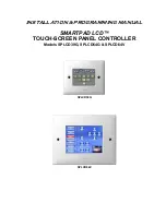
Summary of Contents for ACP-1104

Page 1: ...Multi Touch Panel PC A C P 1 1 0 4 ACP 1104 10 1 Multi Touch Panel PC Intel Celeron Processors RS 232 422 485 USB 3 0 MiniCard HDMI ACP 1104 Manual 1 st Ed May 26 2015...

Page 2: ...is manual is intended to be accurate and reliable However the original manufacturer assumes no responsibility for its use nor for any infringements upon the rights of third parties which may result fr...

Page 3: ...stered trademark of Microsoft Corporation RTL is a trademark of Realtek Semi Conductor Co Ltd C T is a trademark of Chips and Technologies Inc UMC is a trademark of United Microelectronics Corporation...

Page 4: ...he following items have been shipped ACP 1104 Multi Touch Panel PC RJ 45 COM Port Cable x 2 Power Adapter x 1 Product DVD with User s Manual in pdf drivers and utilities VESA Mount Panel Mount If any...

Page 5: ...could cause damage 6 The openings on the device s enclosure are for dissipating heat DO NOT COVER THE OPENINGS 7 Watch out for high temperatures that may occur during system operation 8 Make sure the...

Page 6: ...vious signs of damage displayed on the device 15 DO NOT LEAVE THIS DEVICE IN AN UNCONTROLLED ENVIRONMENT WHERE THE STORAGE TEMPERATURE IS BELOW 10 C 14 F OR ABOVE 60 C 140 F TO PREVENT DAMAGE 16 Exter...

Page 7: ...may not cause harmful interference and 2 this device must accept any interference received including interference that may cause undesired operation Caution There is a danger of explosion if the batte...

Page 8: ...k not classified 2 Degree of protection against the ingress of water IPX1 3 Equipment not suitable for use in the presence of a flammable anesthetic mixture with air or with oxygen or nitrous oxide 4...

Page 9: ...ouch Panel PC A C P 1 1 0 4 Safety Symbol Description The following safety symbols are further explanations for your reference Attention consult ACCOMPANYING DOCUMENTS Ground wire Protective Ground wi...

Page 10: ...Multi Touch Panel PC A C P 1 1 0 4 China RoHS Requirements AAEON Panel PC Workstation Pb Hg Cd Cr VI PBB PBDE O SJ T 11363 2006 X SJ T 11363 2006 ix...

Page 11: ...of Connectors 2 6 2 5 AT ATX Mode Selection JP1 2 7 2 6 LVDS BKLT Control Selection JP2 2 7 2 7 LVDS Power Selection JP3 2 7 2 8 LVDS BKLT Power Selection JP4 2 8 2 9 Clear CMOS Jumper JP5 2 8 2 10 Dr...

Page 12: ...2 2 17 2 23 USB 2 0 Port 3 Connector USB3 2 18 2 24 DDR3L SODIMM Slot DIMM1 2 18 2 25 Half Size MiniCard Slot PCIE1 2 18 2 26 PCI E Full Size MiniCard Slot PCIE2 2 20 2 27 COM to RJ 45 Converter Cable...

Page 13: ...Memory Address Map B 4 B 3 IRQ Mapping Chart B 5 Appendix C Electrical Specifications for I O Ports C 1 Electrical Specifications for I O Ports C 2 C 2 DIO Programming C 3 C 3 Digital I O Register C 4...

Page 14: ...Multi Touch Panel PC A C P 1 1 0 4 General Information Chapter 1 Chapter 1 General Information 1 1...

Page 15: ...iled descriptions and explanations on the product s hardware and software features such as its specifications dimensions jumper connector settings definitions and driver installation instructions to f...

Page 16: ...anel PC A C P 1 1 0 4 1 2 Features 10 1 Multi Touch screen Aluminum Design 7H Two point Multi Touch Display Intel Celeron J1900 N2807 Processor Supports VESA 75 Mounting Interface Chapter 1 General In...

Page 17: ...1 USB 2 0 x 3 LAN x 2 DIO x 6 DI x 4 DO x 2 w o isolation RJ 45 x 2 for RS 232 422 485 BIOS Selection HDMI x 1 Antenna Hole x 2 Power Button x 1 Lockable Power Connector x 1 Storage Device mSATA half...

Page 18: ...t Weight 1 2 kg Gross Weight 2 5 kg Environmental Operating Temperature 32 F 113 F 0 C 45 C mSATA J1900 without airflow 32 F 122 F 0 C 50 C mSATA J1900 with airflow Storage Temperature 5 95 40 o C non...

Page 19: ...isplay Type Max Resolution Max Colors Luminance cd m 2 Contrast Ratio Viewing Angle 10 1 WXGA LED 1280 x 800 262 K 250 nits 600 1 80 H 70 V Touchscreen Type USB Resolution 2048 x 2048 Light Transmissi...

Page 20: ...Multi Touch Panel PC A C P 1 1 0 4 Chapter 2 Hardware Installation 2 1 Hardware Installation Chapter 2...

Page 21: ...hile the power is on because a sudden rush of power can damage sensitive electronic components Always ground yourself to remove any static charge before touching the board Modern electronic devices ar...

Page 22: ...Multi Touch Panel PC A C P 1 1 0 4 Chapter 2 Hardware Installation 2 3 2 2 Mechanical Drawings Front...

Page 23: ...Multi Touch Panel PC A C P 1 1 0 4 Chapter 2 Hardware Installation 2 4 Back...

Page 24: ...that allow you to configure your system to suit your application Label Function JP1 AT ATX Mode Selection JP2 LVDS BKLT Control Selection JP3 LVDS Power Selection JP4 LVDS BKLT Control Selection JP5 C...

Page 25: ...CN1 HDMI Display CN2 USB 3 0 Connector CN4 COM2 RS 232 422 485 CN16 COM3 RS 232 I F CN17 COM1 RS 232 422 485 CN22 BIOS SPI Flash Header CN23 Dry and Wet Contact Digital Input CN24 Dry and Wet Contact...

Page 26: ...P1 1 2 3 ATX Mode Default 1 2 3 AT Mode JP1 Function 1 2 ATX Mode Default 2 3 AT Mode 2 6 LVDS BKLT Control Selection JP2 1 2 3 VR Mode 1 2 3 PWM Mode Default JP2 Function 1 2 VR Mode 2 3 PWM Mode Def...

Page 27: ...5V Default JP4 Function 1 2 12V 2 3 5V Default 2 9 Clear CMOS Jumper JP5 Normal Default Clear CMOS JP5 Function 1 2 Normal Default 2 3 Clear CMOS 2 10 Dry and Wet Contact Digital Input Power Selectio...

Page 28: ...utput Power Selection JP7 1 2 3 Wet Contact Digital Output 1 2 3 Dry Contact Digital Output Default JP7 Function 1 2 Wet Contact Digital Output 2 3 Dry Contact Digital Output Default 2 12 HDMI Display...

Page 29: ...GND 12 HDMI_CLK DIFF 13 NC NC 14 NC NC 15 HDMI_DDC_CLK I O 5V 16 HDMI_DDC_DATA I O 5V 17 GND GND 18 HDMI_PWR PWR 5V 19 HDMI_HPD IN 2 13 USB 3 0 Connector CN2 Pin Pin Name Signal Type Signal Level 1 5V...

Page 30: ...C P 1 1 0 4 Chapter 2 Hardware Installation 2 11 2 14 COM2 RS 232 422 485 Connector CN4 Pin RS 232 RS 422 RS 485 1 DSR 2 RTS 3 GND 4 TX RX 5 RX TX DATA 6 DCD TX DATA 7 CTS 8 DTR RX 2 15 COM3 RS 232 I...

Page 31: ...P 1 1 0 4 Chapter 2 Hardware Installation 2 12 2 DSR 3 RX 4 RTS 5 TX 6 CTS 7 DTR 8 RI 9 GND 2 16 COM1 RS 232 422 485 Connector CN17 Pin RS 232 RS 422 RS 485 1 DSR 2 RTS 3 GND 4 TX RX 5 RX TX DATA 6 DC...

Page 32: ...Multi Touch Panel PC A C P 1 1 0 4 Chapter 2 Hardware Installation 2 13 2 17 Dry and Wet Contact Digital Input CN23...

Page 33: ...PC A C P 1 1 0 4 Chapter 2 Hardware Installation 2 14 Digital input voltage range Max 10 25V Min 5V Pin Pin Name Signal Type Signal Level 1 Digital input 3 Input DRY 5V WET 3 30V Wet Contact Wiring D...

Page 34: ...nput DRY 5V WET 3 30V 4 Digital input 0 Input DRY 5V WET 3 30V 5 WET contact POWER PWR 3 30V 2 18 Dry and Wet Contact Digital Output CN24 Digital output voltage range Max 30V Min 5V Pin Pin Name Signa...

Page 35: ...output 4 Input Open collector to 30 VDC 4 Digital output POWER Input 3 30 V 5 GND GND 2 19 RJ 45 Ethernet Port CN26 Pin Pin Name Signal Type Signal Level 1 MDI0 DIFF 2 MDI0 DIFF 3 MDI1 DIFF 4 MDI2 DI...

Page 36: ...MDI0 DIFF 3 MDI1 DIFF 4 MDI2 DIFF 5 MDI2 DIFF 6 MDI1 DIFF 7 MDI3 DIFF 8 MDI3 DIFF 2 21 USB 2 0 Port 1 Connector USB1 Pin Pin Name Signal Type Signal Level 1 5V PWR 5V 2 USB_D DIFF 3 USB_D DIFF 4 GND G...

Page 37: ...Pin Pin Name Signal Type Signal Level 1 5V PWR 5V 2 USB_D DIFF 3 USB_D DIFF 4 GND GND 2 24 DDR3L SODIMM Slot DIMM1 Standard Specification 2 25 Half Size MiniCard Slot PCIE1 Pin Pin Name Signal Type S...

Page 38: ...NC 14 NC 15 GND GND 16 NC 17 NC 18 GND GND 19 NC 20 NC 21 GND GND 22 NC 23 mSATA RX DIFF 24 3 3V PWR 3 3V 25 mSATA RX DIFF 26 GND GND 27 GND GND 28 1 5V PWR 1 5V 29 GND GND 30 SMB_CLK I O 3 3V 31 mSAT...

Page 39: ...7 GND GND 38 NC 39 3 3V PWR 3 3V 40 GND GND 41 3 3V PWR 3 3V 42 NC 43 NC 44 NC 45 NC 46 NC 47 NC 48 1 5V PWR 1 5V 49 NC 50 GND GND 51 NC 52 3 3V PWR 3 3V 2 26 PCI E Full Size MiniCard Slot PCIE2 Pin P...

Page 40: ...are Installation 2 21 6 1 5V PWR 1 5V 7 NC 8 NC 9 GND GND 10 NC 11 NC 12 NC 13 NC 14 NC 15 GND GND 16 NC 17 NC 18 GND GND 19 NC 20 NC 21 GND GND 22 NC 23 PCIE RX DIFF 24 3 3V PWR 3 3V 25 PCIE RX DIFF...

Page 41: ...ation 2 22 30 SMB_CLK I O 3 3V 31 PCIE TX DIFF 32 SMB_DATA I O 33 PCIE TX DIFF 34 GND GND 35 GND GND 36 NC 37 GND GND 38 NC 39 3 3V PWR 3 3V 40 GND GND 41 3 3V PWR 3 3V 42 NC 43 NC 44 NC 45 NC 46 NC 4...

Page 42: ...h Panel PC A C P 1 1 0 4 Chapter 2 Hardware Installation 2 23 2 27 COM to RJ 45 Converter Cable For COM1 COM2 Pin RS 232 RS 422 RS 485 1 DCD TX DATA 2 RXD TX DATA 3 TXD RX 4 DTR RX 5 GND 6 DSR 7 RTS 8...

Page 43: ...et the wallmount brackets and sponge ready Wall mount bracket Sponge Step 2 Remove the six screws three on each side at the back and place the wallmount brackets onto the panel Secure the brackets wit...

Page 44: ...ep 4 Insert the display to the surface opening where you are going to mount the panel 2 wall Step 5 Attach the mounting clips to the four fillisters on the wallmount brackets and tighten the four M4x6...

Page 45: ...Multi Touch Panel PC A C P 1 1 0 4 AMI BIOS Setup Chapter 3 Chapter 3 AMI BIOS Setup 3 1...

Page 46: ...S NVRAM If system configuration is not found or system configuration data error is detected system will load optimized default and re boot with this default system configuration automatically There ar...

Page 47: ...tup information when the power is turned off Entering Setup Power on the computer and press Del immediately This will allow you to enter Setup Main Set the date use tab to switch between date elements...

Page 48: ...Multi Touch Panel PC A C P 1 1 0 4 Setup Menu Setup submenu Main Chapter 3 AMI BIOS Setup 3 4...

Page 49: ...Multi Touch Panel PC A C P 1 1 0 4 Setup submenu Advanced Chapter 3 AMI BIOS Setup 3 5...

Page 50: ...PC A C P 1 1 0 4 CPU Configuration Options summary Intel Virtualization Technology Disabled Enabled Optimal Default Failsafe Default EIST Disabled Enabled Optimal Default Failsafe Default Chapter 3 A...

Page 51: ...Multi Touch Panel PC A C P 1 1 0 4 IDE Configuration IDE Options summary SATA Mode IDE Mode AHCI Mode Optimal Default Failsafe Default Chapter 3 AMI BIOS Setup 3 7...

Page 52: ...USB Support Enabled Optimal Default Failsafe Default Disabled Auto Enables BIOS Support for Legacy USB Support When enabled USB can be functional in legacy environment like DOS AUTO option disables l...

Page 53: ...Multi Touch Panel PC A C P 1 1 0 4 Hardware Monitor Chapter 3 AMI BIOS Setup 3 9...

Page 54: ...P 1 1 0 4 Dynamic Digital IO Options summary GPO0 Direction Output Output Level Low Hi Optimal Default Failsafe Default GPO1 Direction Output Output Level Low Hi Optimal Default Failsafe Default Chapt...

Page 55: ...er Loss Last State Optimal Default Failsafe Default Power On Power Off Select power state when power is re applied after a power failure RTC wake system from S5 Disabled Optimal Default Failsafe Defau...

Page 56: ...Multi Touch Panel PC A C P 1 1 0 4 SIO Configuration Chapter 3 AMI BIOS Setup 3 12...

Page 57: ...Disabled Enabled Optimal Default Failsafe Default En Disable Serial Port COM Possible Use Automatic Settings Optimal Default Failsafe Default IO 3F8 IRQ 4 IO 2F8 IRQ 3 Select an optimal setting for I...

Page 58: ...Disabled Enabled Optimal Default Failsafe Default En Disable Serial Port COM Possible Use Automatic Settings Optimal Default Failsafe Default IO 2F8 IRQ 3 IO 3F8 IRQ 4 Select an optimal setting for I...

Page 59: ...ons summary Use This Device Disabled Enabled Optimal Default Failsafe Default En Disable Serial Port COM Possible Use Automatic Settings Optimal Default Failsafe Default IO 3E8 IRQ 11 IO 2E8 IRQ 11 Se...

Page 60: ...Multi Touch Panel PC A C P 1 1 0 4 Setup submenu Chipset Chapter 3 AMI BIOS Setup 3 16...

Page 61: ...Multi Touch Panel PC A C P 1 1 0 4 North Bridge Chapter 3 AMI BIOS Setup 3 17...

Page 62: ...onfiguration Options summary DVMT Pre Allocated 64M Optimal Default Failsafe Default 96M 128M 160M 192M 224M 256M 288M 320M 352M 384M 416M 448M 480M 512M DVMT Total Gfx Mem 128MB 256MB Optimal Default...

Page 63: ...Multi Touch Panel PC A C P 1 1 0 4 South Bridge Options summary Audio Controller Disabled Enabled Optimal Default Failsafe Default Chapter 3 AMI BIOS Setup 3 19...

Page 64: ...a dialog box appears which lets you enter a password You can enter no more than six letters or numbers Press Enter after you have typed in the password A second dialog box asks you to retype the pass...

Page 65: ...s summary Quiet Boot Disabled Enabled Default En Disable showing boot logo Option ROM Messages Force BIOS Default Keep Current Set display mode for Option ROM Launch PXE OpROM Disabled Default Enabled...

Page 66: ...Multi Touch Panel PC A C P 1 1 0 4 BBS Priorities Chapter 3 AMI BIOS Setup 3 22...

Page 67: ...Multi Touch Panel PC A C P 1 1 0 4 Setup submenu Exit Chapter 3 AMI BIOS Setup 3 23...

Page 68: ...Multi Touch Panel PC A C P 1 1 0 4 Driver Installation Chapter 4 Chapter 4 Driver Installation 4 1...

Page 69: ...t please follow the sequence below to install the drivers Follow the sequence below to install the drivers Step 1 Install Chipset Driver Step 2 Install Graphics Driver Step 3 Install Network Driver S...

Page 70: ...cally Step 2 Install Graphics Driver 1 Open the Step 2 Graphics folder and select your OS 2 Open the Setup exe file in the folder 3 Follow the instructions 4 Drivers will be installed automatically St...

Page 71: ...Windows 8 1 only 1 Open the Step 5 Intel Sideband Fabric Device followed by the Setup exe file 2 Follow the instructions 3 Drivers will be installed automatically Step 6 Install Touch Driver 1 Open th...

Page 72: ...Multi Touch Panel PC A C P 1 1 0 4 Programming the Watchdog Timer Appendix A Appendix A Programming the Watchdog Timer A 1...

Page 73: ...ote24 Time of watchdog timer 0 255 This register is byte access Counting Unit 0x07 Note5 0xF5 Note6 3 Note7 0 Note8 Select time unit 0 second 1 minute Watchdog Enable 0x07 Note9 0xF5 Note10 5 Note11 1...

Page 74: ...byte EnableLDN This parameter is represented from Note9 define byte EnableReg This parameter is represented from Note10 define byte EnableBit This parameter is represented from Note11 define byte Ena...

Page 75: ...ure AaeonWDTConfig byte Timer Time of WDT timer 0x00 0xFF boolean Unit Select time unit 0 second 1 minute AaeonWDTConfig Procedure AaeonWDTEnable This procudure will enable the WDT counting AaeonWDTEn...

Page 76: ...g VOID WDTEnableDisable byte LDN byte Register byte BitNum byte Value SIOBitSet LDN Register BitNum Value VOID WDTParameterSetting Watchdog Timer counter setting SIOByteSet TimerLDN TimerReg TimerVal...

Page 77: ...VOID SIOBitSet byte LDN byte Register byte BitNum byte Value Byte TmpValue SIOEnterMBPnPMode SIOSelectLDN byte LDN IOWriteByte SIOIndex Register TmpValue IOReadByte SIOData TmpValue 1 BitNum TmpValue...

Page 78: ...Multi Touch Panel PC A C P 1 1 0 4 I O Information Appendix B Appendix B I O Information B 1...

Page 79: ...Multi Touch Panel PC A C P 1 1 0 4 B 1 I O Address Map Appendix B I O Information B 2...

Page 80: ...Multi Touch Panel PC A C P 1 1 0 4 Appendix B I O Information B 3...

Page 81: ...Multi Touch Panel PC A C P 1 1 0 4 B 2 Memory Address Map Appendix B I O Information B 4...

Page 82: ...Multi Touch Panel PC A C P 1 1 0 4 B 3 IRQ Mapping Chart Appendix B I O Information B 5...

Page 83: ...Multi Touch Panel PC A C P 1 1 0 4 Appendix B I O Information B 6...

Page 84: ...Multi Touch Panel PC A C P 1 1 0 4 Appendix B I O Information B 7...

Page 85: ...Multi Touch Panel PC A C P 1 1 0 4 Appendix B I O Information B 8...

Page 86: ...Multi Touch Panel PC A C P 1 1 0 4 Electrical Specifications for I O Ports Appendix C Appendix C Electrical Specifications for I O Ports C 1...

Page 87: ...HDMI Connector CN1 5V 5V 1A USB3 0 Connector USB3 5V 5V 1Aer channel mSATA Connector PCIE1_A1 3 3VSB 1 5V 3 3V 1 1A 1 5V 0 375A COM1 RS232 422 485 Connector CN17 5V 12V 5V 0 5A or 12V 0 5A COM2 RS232...

Page 88: ...gram is also attached based on which you can develop customized program to fit your application There are three steps to complete the configuration setup 1 Enter the MB PnP Mode 2 Modify the data of c...

Page 89: ...in Status 0x06 Note12 0xA2 Note13 3 Note14 GPIO53 DIO 5 Pin Status 0x06 Note15 0xA2 Note16 4 Note17 GPIO54 DIO 5 Pin Status 0x06 Note18 0xA2 Note19 5 Note20 GPIO55 Table 3 Digital Output relative regi...

Page 90: ...om Note7 define byte DInput2Bit This parameter is represented from Note8 define byte DInput3LDN This parameter is represented from Note9 define byte DInput3Reg This parameter is represented from Note1...

Page 91: ...byte DOutput3Bit This parameter is represented from Note31 define byte DOutput3Val This parameter is represented from Note32 define byte DOutput4LDN This parameter is represented from Note33 define b...

Page 92: ...utput InputStatus 0 Digital I O Pin level is low 1 Digital I O Pin level is High PinStatus AaeonReadPinStatus DInput3LDN DInput3Reg DInput3Bit Procedure AaeonSetOutputLevel Input Example Set Digital I...

Page 93: ...te BitNum Boolean PinStatus PinStatus SIOBitRead LDN Register BitNum Return PinStatus VOID AaeonSetOutputLevel byte LDN byte Register byte BitNum byte Value ConfigToOutputMode LDN Register BitNum SIOB...

Page 94: ...SIOBitSet byte LDN byte Register byte BitNum byte Value Byte TmpValue SIOEnterMBPnPMode SIOSelectLDN byte LDN IOWriteByte SIOIndex Register TmpValue IOReadByte SIOData TmpValue 1 BitNum TmpValue Valu...

Page 95: ...e 1 BitNum SIOExitMBPnPMode If TmpValue 0 Return 0 Return 1 VOID ConfigToOutputMode byte LDN byte Register byte BitNum Byte TmpValue OutputEnableReg OutputEnableReg Register 1 SIOEnterMBPnPMode SIOSel...

Reviews: