12
Fox (LP3500)
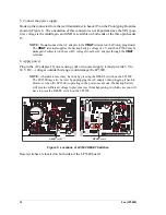
5. Connect the power supply.
Hook up the connector from the wall transformer to header J5 on the Prototyping Board as
shown in Figure 4. The orientation of this connector is not important since the VIN (posi-
tive) voltage is the middle pin, and GND is available on both ends of the three-pin header
J5.
NOTE:
Do
not
connect the AC adapter to the
VBAT
terminal on the Prototyping Board.
The
VBAT
terminal supplies the backup battery voltage of 3 V, and the LP3500 may be
damaged if subjected to the raw DC voltage from the AC adapter through the
VBAT
terminal.
6. Apply power.
Plug in the AC adapter. If you are using your own power supply, it must provide 3 V to
30 V DC—voltages outside this range could damage the LP3500.
NOTE:
A hardware reset may be done by pressing the RESET switch on the LP3500.
The LP3500 may also be reset by unplugging the AC adapter, then plugging it back in.
However, when the LP3500 is operating in the power-save mode, the backup battery
will provide sufficient voltage to prevent a reset from happening, in which case you will
have to press the RESET switch on the LP3500.
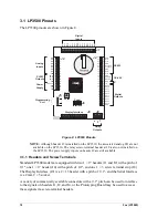
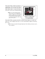
Figure 5. Locations of LP3500 RESET Switches
Reset switches are located on both sides of the LP3500 board.
C44
C43
C59
C60
U9
R16
R13
C10
C13
R17
R18
C16
C19
C36
U1
C70
R51
R58
C65
C26 C33
R20 R25
R22 R26
R29
C37
R32
C40
Y1
D22
C50 R36 R40 C54
R37
C24
R30
D19
D20
D21
D18
D25
Q5
R42
Q6
R43
R33
Q8
Q10
D26
D28
Q16
D30
Q17
D34
K1
Q13
D32
D33
Q14
J6
C67
C55 R44
R47
U11
S1
RESET
J5
J2
PROGRAM
PORT
AIN0 AIN1
A
I
N2
AIN3 AIN4 AIN5 AIN6 AIN7 GND
GNDVBAT
EXT GND VIN GND
PWM0
PWM
1
PWM2
GND
DISPLA
Y
R55
R56
J9
J8
RELAY
NO
COM
NC
PROGRAM
PORT
TP2
/RESET
RESET
JP1
JP2
JP3
JP4
JP5
JP6
JP8
JP1
1
JP7
JP10
JP9
JP12
RP1
D3
RP2
D6
D12
D10
RP4
RP3
D16
D14
Q3
Q4
D23
D24
Q7
D27
Q9
RP10
D29
Q11
D31
Q15
RP12
RP11
Q21
Q19
Q18
PROGRAM
PORT
TP2
/RESET
RESET
S2
R14
C14
R15
C9
R5
R8
C27
R19
R21
R27
R24
C34
R28
C38
R35
C25
C31
C18
C28
C30
RP9
RP8
R59
C49
R52
R53
C63
R46
U2
815 07 IN
R10
R11
R12
R2
R3
R4
+K
GND
VCC
RP15
D6
D4
D2
D0
A1
A3
GND
DPRST
D7
D5
D3
D1
A0
A2
GND
GND
DISP
VDISP
OUT0
OUT1
OUT2
OUT3
OUT4
OUT5
OUT6
OUT7
OUT8
OUT9
GND
GND +K
GND RxE TxE GND RxC
TxC GND RxB TxB GND + 485
CTS RTS
IN00
IN01
IN02
IN03
IN04
IN05
IN06
IN07
GND
IN08
IN09
IN10
IN11
IN12
IN13
IN14
IN15
C4
C1
U4
TP1
VRAM
U5
C39
420 mA
AIN3
AIN2
AIN1
AIN0
GND
VIN
GND
GND
PWM
2
PWM
1
PWM
0
GND
AIN7
AIN6
AIN5
AIN4
AIN3
AIN2
AIN1
AIN0
VBAT
EXT
C52
R60
C71
C21
JP13
IN DR OUT
J6
C48
U3
R57
R31
C29
R23
C22
C20
C12
C15
D15
D17
RP17
D13
BT1
D1
1
D5
D7
D2
D4
C8
C6
D8
D1
AIN0 AIN1 AIN2 AIN3
J3
R1
C3
C2
R6
R7
R9
Q22
RN1
RN2
Battery
R54
RP14
RP13
Q20
U13
C64
R50
R49
Y2
C61
Q12
R45
R34
U8
C51
R39
R41
C53
R38
R48
C66
U12
U10
GND
+K GND 485 + GND TxB RxB GND
TxC RxC GND TxE RxE GND
J4
J1
OUT9
OUT8
OUT7
OUT6
OUT5
OUT4
OUT3
OUT2
OUT0
OUT
1
IN00 IN01 IN02 IN03 IN04 IN05 IN06 IN07
GND
IN08 IN09 IN10 IN1
1 IN12 IN13 IN14 IN15
RESET
switch
U7
RESET
switch
U6
U7
C42
C41
D9
C7
C5
C69
C68
C23
C17
Summary of Contents for Fox LP3500
Page 1: ...Fox LP3500 C Programmable Single Board Computer User s Manual 019 0111 041029 E ...
Page 6: ...Fox LP3500 ...
Page 14: ...8 Fox LP3500 ...
Page 22: ...16 Fox LP3500 ...
Page 86: ...80 Fox LP3500 ...
Page 120: ...114 Fox LP3500 ...
Page 130: ...124 Fox LP3500 ...
Page 134: ...128 Fox LP3500 ...
Page 138: ...132 Fox LP3500 ...
Page 142: ...136 Fox LP3500 ...
Page 144: ......

