


2-2
IM 704610-01E
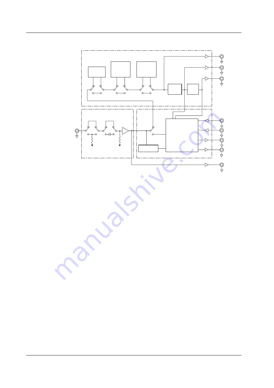
Block Diagram
RF input
Input circuit
Measurement/computation circuit
Equalizer circuit
Time measurement
and
measurement control
AGC
Equalizer
Slicer
PLL
EQUALIZED
OUT
SLICED RF
OUT
CLOCK
OUT
EXT ARM
IN
INHIBIT
IN
JITTER
DC OUT
DC clamp
1 M
Ω
MONITOR
OUT
50
Ω
LEVEL
DC OUT
Level
measurement
AC/DC
The TA220 is a jitter measuring instrument that utilizes signal processing circuits (auto slicer, equalizer,
and PLL) for support of the Blu-ray Disk standard (hereinafter, BD) of next-generation high precision
optical discs. When BD-standard RF signals are input to the instrument, the PLL circuit regenerates the
clock signal enabling measurement of the data to clock (D-to-C) jitter.
The RF signals input to the measurement input terminal (RF input) are routed through the input circuit at
the selected input coupling and input impedance, and are passed to the measurement/computation circuit
via a buffer amplifier. At the same time, signals passing through the input circuit are output from the RF
signal monitoring output terminal (MONITOR OUT) on the rear panel.
The amplitude of the signals coming from the input circuit is measured by the level measurement circuit.
The measured amplitude values are processed by the computation circuit and are sent to Display 1 (the 7-
segment red LED) for display. These amplitude values can also be converted to DC voltages between 0
and 5 V, and output from the voltage level DC output terminal (LEVEL DC OUT) on the rear panel.
The RF signals passing through the input circuit are routed to the equalizer circuit if the equalizer circuit is
selected. Otherwise, they are sent directly to the measurement/computation circuit.
When the equalizer circuit is selected, the RF signals pass through the DC clamp circuit (DC clamp), AGC
amplifier (AGC), and variable boost equalizer circuits (equalizer), and are converted to binary values by the
autoslice (slicer) circuit. Binarized data signals are input to the PLL circuit (PLL), and the clock signal is
regenerated. Data and clock signals are input to the measurement/computation circuit where the D-to-C
time (phase difference) is measured and jitter values are calculated. RF signals prior to binarization that
are processed in the equalizer are output from the equalized RF signal monitoring output terminal
(EQUALIZED OUT) on the rear panel, or, data signals and clock signals are output from the data signal
output terminal (SLICED RF OUT) and clock signal output terminal (CLOCK OUT) on the rear panel,
respectively.
The DC clamp circuit function is used to stabilize input RF signals with DC components such as can occur
with mirror portions of discs. This circuit temporarily adjusts the low-band cutoff frequency from 10 kHz to
3 MHz, thereby quickly attenuating the fluctuating DC component. The DC clamp circuit is active during
the inhibit period.
The variable boost equalizer circuit has the equalizing characteristics shown by the transfer function below,
and the characteristics of a 3rd order Bessel LPF (lowpass filter, 3 dB attenuation point 30 MHz)
connected in cascade. You can set the difference in gain at 100 kHz and 16.5 MHz as the boost amount.
H(z)=1/2{–k+(1+k)z
–1
+(1+k)z
–2
–kz
–3
}
The autoslice circuit consists of a first order integration feedback circuit. It uses a function that superimposes
DC voltage on the slice level, and you can change the slice level when the RF signal is binarized.
In the measurement/computation circuit, signal acquisition is controlled according to external arming and
inhibit signals (EXT ARM and INHIBIT), time measurement and computation is performed on the acquired
data, and jitter, jitter ratio, and average values are calculated. The results are shown by the meter needle
and the value displayed on Display 1. In addition, the jitter ratio can also be converted to a DC voltage
between 0 and 5 V, and output from the jitter ratio DC output terminal (JITTER DC OUT) on the rear panel.
2.1 System Configuration and Block Diagram