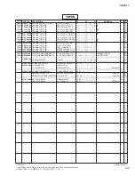


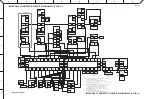

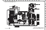

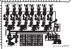
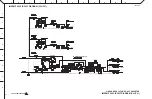

CL3/CL1
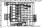
H G F E D C B A
1
2
3
4
5
6
14
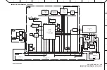
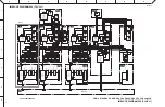
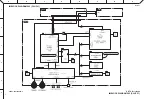
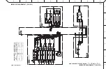
■
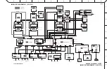
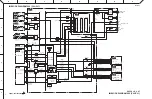
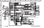
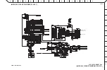
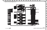
OVERALL CONNECTOR CIRCUIT DIAGRAM 001 (CL3/CL1)
■
OVERALL CONNECTOR CIRCUIT DIAGRAM 001 (CL3/CL1)
AC
DC
DA
OPT
LCDC
DNTU
HAAD
TBPHN
DCMS
USB
FD8CN
PNENR
PNENL
PNMB
FD8
FD8
CPU
FX
JK
DSP
PN8
PN8
PNI
PN8
PNM
PN2
FD2
3
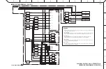
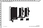
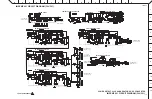
CONNECTOR ASSEMBLY (See page 15)
2 PH&PH 4P, 6P, 10P (See page 15)
1 RECEPTACLE M7CL
(See page 15)
Note2) In the drawing, the symbol shows an FFC connector by which 1Pin is
connected to nPin, 2Pin to (n-1)Pin, ..., and nPin to 1Pin.
Where, nPin is the maximum number of pins in the connector.
Other connector connects 1Pin to 1Pin and nPin to nPin.
Note1) The connection of the part marked with an (digits) on the wire will be
described in detail on pages 15.
Other part has an one-to-one relation with a connector.
CL3: LAMP x 2
CL1: LAMP x 1
CL3 only
28CA2-2001101589-1
Summary of Contents for CL3
Page 7: ...7 CL3 CL1 DIMENSIONS CL3 CL1 648 15 201 130 299 667 839 15 201 130 299 667 Unit mm...
Page 95: ...95 CL3 CL1 CPU Circuit Board Pattern side to DSP CN101 2NA WY67750 1...
Page 101: ...101 CL3 CL1 DNTU Circuit Board Pattern side Scale 80 100 2NA WZ20390 5...
Page 102: ...CL3 CL1 102 2NA WY63530 FX Circuit Board WR 63 1 Component side Scale 95 100...
Page 103: ...103 CL3 CL1 2NA WY63530 FX Circuit Board Pattern side Scale 95 100...
Page 105: ...105 CL3 CL1 HAAD Circuit Board Pattern side Scale 90 100 2NA WY64340 2...
Page 107: ...107 CL3 CL1 2NA WY63490 Component side JK Circuit Board WR 63 1...
Page 109: ...109 CL3 CL1 Component side TBPHN Circuit Board WR 06 1 WR 63 1 2NA WY64360 1...
Page 110: ...CL3 CL1 110 Component side PN8 Circuit Board to FD8 CN902 or FD8CN CN902 2NA WY53120 2...
Page 118: ...CL3 CL1 118 Component side PNENL Circuit Board to PN8 CN001 2NA WY53130 1...
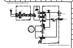
Page 160: ...CL3 CL1 160 1 18 LCD Test LCD LCD 1 3 2 9 5 OK NG 1 2 H 3 O X O 4 BOX 5x4...
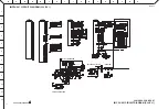
Page 382: ...7 MBCL CIRCUIT BOARDS A A A A 2NA WY53200 1 MB Circuit Board Component side...
Page 383: ...MBCL 8 MB Circuit Board DSUB PH CONNECTOR ASSEMBLY B B B B 2NA WY53200 1 Pattern side...


