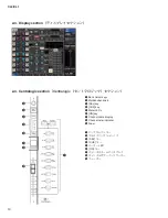


20
CL3/CL1
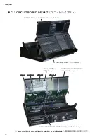
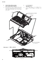
Fig. 1 (図 1)
■
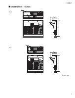
CL3 DISASSEMBLY PROCEDURE
(分解手順)
Precaution
(注意事項)
Take care not to trap your fi ngers.
作業中は指を挟まない様に注意してください。
* Install the filament tape and the harness clamp in
the same way as they were before removal.
※ フィラメントテープ、束線止めは、取り外す前と同じ
ように取り付けてください。
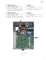
*
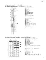
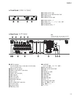
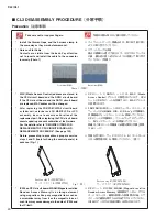
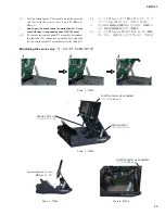
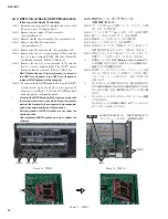
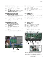
Notes on Flat Cable
Contacts are visible from the back. Pay attention
not to insert and install the cable to the connector
inversely. (Photo 1)
※ フラットケーブル注意
接点が裏面から透けて見えます。コネクタにケーブル
の表・裏を逆に差し込まないように注意して取り付け
てください。(写真 1)
Front side (
表面
)
Back side (
裏面
)
* MAC (Media Access Control) address are stored in
the CPU circuit board and the DNTU circuit board.
If the CPU circuit board and the DNTU circuit board
are replaced, MAC address will be changed.
※ CPU シ ー ト と DNTU シ ー ト に は、MAC(Media
Access Control)アドレスが設定されています。CPU
シートと DNTU シートを交換すると、MAC アドレス
が変更されます。
*
After replacing the FD8/FD8CN/FD2 circuit board
or fader unit, color bar and CH MAME LCD, or LCD
a s s e m bly, b e s u r e t o exe c u t e c a l i b r a t i o n o f t h e
replacement part. When replacing the CPU circuit board,
execute updating and each calibration of the fi rmware.
For the details, refer to “REQUIRED ITEMS FOR
REPLACEMENT OF CPU CIRCUIT BOARD AND
REPLACEMENT PROCEDURE”. (See page 192)
※ FD8/FD8CN/FD2 シート又はフェーダーユニット、カ
ラーバーと CH NAME LCD、LCD Ass y の交換後は、
交換部品のキャリブレーションを実施してください。
CPU シートの交換時は、ファームウェアのアップデー
ト、各キャリブレーションを実施してください。
詳細は、
「CPU シート交換後に必要な項目と手順」参照。
(193 ページ)
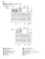
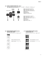
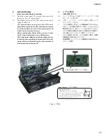
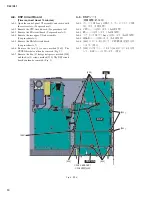
* Before proceeding to procedures, prepare service
stays L and R (tools for fi xing the control panels) in
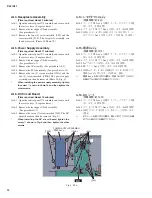
advance. (Fig. 1)
※ 作業を行う前に、サービスステイ L、R (コントロール
パネル固定用工具)を用意してください。(図1)
Service stay L (WZ987700)
サービスステイ L (WZ987700)
Service stay R (WZ987800)
サービスステイ R (WZ987800)
*
IC204 on CPU circuit board: MRAM (Magneto resistive
Random Access Memory) is a storage element
using magnetism. Keep any magnetic item such as
a screwdriver away from it as the magnetic force of
such item may cause damage to the data of IC204 and
the IC itself.
※ CPU シ ー ト の IC204:MRAM (Magneto resistive
Random Access Memory:磁気抵抗ランダム・アクセ
ス・メモリー ) は、磁気を利用した記憶素子の為、ドラ
イバーなど磁気を帯びたものを近づけないでください。
IC204 のデータや IC 自身が壊れる恐れがあります。
Photo 1 (写真 1)
Summary of Contents for CL3
Page 7: ...7 CL3 CL1 DIMENSIONS CL3 CL1 648 15 201 130 299 667 839 15 201 130 299 667 Unit mm...
Page 95: ...95 CL3 CL1 CPU Circuit Board Pattern side to DSP CN101 2NA WY67750 1...
Page 101: ...101 CL3 CL1 DNTU Circuit Board Pattern side Scale 80 100 2NA WZ20390 5...
Page 102: ...CL3 CL1 102 2NA WY63530 FX Circuit Board WR 63 1 Component side Scale 95 100...
Page 103: ...103 CL3 CL1 2NA WY63530 FX Circuit Board Pattern side Scale 95 100...
Page 105: ...105 CL3 CL1 HAAD Circuit Board Pattern side Scale 90 100 2NA WY64340 2...
Page 107: ...107 CL3 CL1 2NA WY63490 Component side JK Circuit Board WR 63 1...
Page 109: ...109 CL3 CL1 Component side TBPHN Circuit Board WR 06 1 WR 63 1 2NA WY64360 1...
Page 110: ...CL3 CL1 110 Component side PN8 Circuit Board to FD8 CN902 or FD8CN CN902 2NA WY53120 2...
Page 118: ...CL3 CL1 118 Component side PNENL Circuit Board to PN8 CN001 2NA WY53130 1...
Page 160: ...CL3 CL1 160 1 18 LCD Test LCD LCD 1 3 2 9 5 OK NG 1 2 H 3 O X O 4 BOX 5x4...
Page 382: ...7 MBCL CIRCUIT BOARDS A A A A 2NA WY53200 1 MB Circuit Board Component side...
Page 383: ...MBCL 8 MB Circuit Board DSUB PH CONNECTOR ASSEMBLY B B B B 2NA WY53200 1 Pattern side...


