
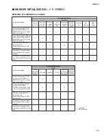
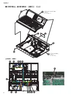
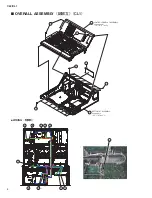

192
CL3/CL1
■
REQUIRED ITEMS FOR REPLACEMENT OF CPU CIRCUIT BOARD
AND REPLACEMENT PROCEDURE
1) Calibrations
Fader calibration:
See page 170 of Service Manual.
Touch screen calibration:
See page 168 of Service Manual
Channel Color Calibration:
See page 172 of Service Manual
* After replacing the parts of LCD assembly, color bar and CH NAME LCD, FD8/FD8CN/FD2 circuit board and fader unit,
be sure to execute calibration of the replacement parts.
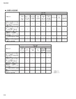
2)
Updating Firmware
See page 164.
The service parts are not subject to the fi rmware control. After their replacement, be sure the upgrade the version to the latest
fi rmware.
3)
Inputting Model Name
The CPU circuit board is commonly usable with CL1, CL3 and CL5. To identify the part for each model, write the model
identifi cation fi le on the CPU circuit board when updating the fi rmware, using the following procedure.
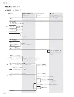
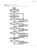
Writing Procedure
4)
Copy the fi le of the applicable model to the root directory of the USB STORAGE.
Download the fi les from YSISS. (Do not put a multiple number of fi les together.)
• CL5: CL5NAME.BIN
• CL3: CL3NAME.BIN
• CL1: CL1NAME.BIN
5)
Insert the USB memory into the USB terminal of the CL main unit and turn on the power.
6)
If the program of the main unit is activated, writing has been completed. (Nothing like a confi rmation message appears be-
fore writing.)
• Once the model name has been written, it is not necessary to write again unless cleared by accident.
• Updating the fi rmware and writing of the model name can be executed at the same time.
• Even if updating is cancelled, the model name will be written. (It is not possible to cancel writing of the model name.)
• Unless necessary, delete the fi le of the above model name: CL5/3/1 NAME. BIN from the USB. (Or, writing will be necessary
every time updating the program.)
7)
Set the date and time of the internal clock. See page 35 of Owner’s Manual
Summary of Contents for CL3
Page 7: ...7 CL3 CL1 DIMENSIONS CL3 CL1 648 15 201 130 299 667 839 15 201 130 299 667 Unit mm...
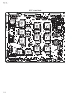
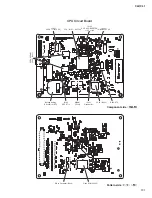
Page 95: ...95 CL3 CL1 CPU Circuit Board Pattern side to DSP CN101 2NA WY67750 1...
Page 101: ...101 CL3 CL1 DNTU Circuit Board Pattern side Scale 80 100 2NA WZ20390 5...
Page 102: ...CL3 CL1 102 2NA WY63530 FX Circuit Board WR 63 1 Component side Scale 95 100...
Page 103: ...103 CL3 CL1 2NA WY63530 FX Circuit Board Pattern side Scale 95 100...
Page 105: ...105 CL3 CL1 HAAD Circuit Board Pattern side Scale 90 100 2NA WY64340 2...
Page 107: ...107 CL3 CL1 2NA WY63490 Component side JK Circuit Board WR 63 1...
Page 109: ...109 CL3 CL1 Component side TBPHN Circuit Board WR 06 1 WR 63 1 2NA WY64360 1...
Page 110: ...CL3 CL1 110 Component side PN8 Circuit Board to FD8 CN902 or FD8CN CN902 2NA WY53120 2...
Page 118: ...CL3 CL1 118 Component side PNENL Circuit Board to PN8 CN001 2NA WY53130 1...
Page 160: ...CL3 CL1 160 1 18 LCD Test LCD LCD 1 3 2 9 5 OK NG 1 2 H 3 O X O 4 BOX 5x4...
Page 382: ...7 MBCL CIRCUIT BOARDS A A A A 2NA WY53200 1 MB Circuit Board Component side...
Page 383: ...MBCL 8 MB Circuit Board DSUB PH CONNECTOR ASSEMBLY B B B B 2NA WY53200 1 Pattern side...


