background image

1

VX-450 Series UHF Band Service Manual

Introduction

This manual provides the technical information necessary for servicing the VX-450 Series Transceiver.

Servicing this equipment requires expertise in handing
surface-mount chip components. Attempts by non-quali-
fied persons to service this equipment may result in per-
manent damage not covered by the warranty, and may be
illegal in some countries.

Two PCB layout diagrams are provided for each double-
sided board in this transceiver. Each side of the board is
referred to by the type of the majority of components in-
stalled on that side (“Side A” or “Side B”). In most cases
one side has only chip components (surface-mount de-
vices), and the other has either a mixture of both chip and
leaded components (trimmers, coils, electrolytic capacitors,
ICs, etc.), or leaded components only.

As described in the pages to follow, the advanced micro-
processor design of the VX-450 Series Transceiver allows a
complete alignment of this transceiver to be performed without opening the case of the radio; all adjustments can be
performed from the front panel, using the “Alignment Mode” menu.

While we believe the information in this manual to be correct, VERTEX STANDARD assumes no liability for damage that
may occur as a result of typographical or other errors that may be present. Your cooperation in pointing out any inconsis-
tencies in the technical information would be appreciated.

Important Note

This transceiver is assembled using Pb (lead) free solder, based on the RoHS specification.
Only lead-free solder (Alloy Composition: Sn-3.0Ag-0.5Cu) should be used for repairs performed on this apparatus. The
solder stated above utilizes the alloy composition required for compliance with the lead-free specification, and any solder with
the above alloy composition may be used.

Specifications ................................................................... 2

USA (NA) & Except EIA (CE) Models ...................... 2
EIA (CE) Model .......................................................... 3

Exploded View & Miscellaneous Parts ......................... 4

16 key & 4 key Type ................................................... 4
Non key Type .............................................................. 5

Parts List .......................................................................... 6
Block Diagram ................................................................ 8

Version A & D ............................................................ 8
Version I & K ............................................................ 16

Circuit Description ....................................................... 24

Version A & D .......................................................... 24
Version I & K ............................................................ 27

Alignment ...................................................................... 30
Board Units (Schematics & Layouts)

MAIN Unit (Version A & D) ................................... 44

16 key & 4 key Type ........................................... 44
Non key Type ...................................................... 53

MAIN-2 Unit (Version I & K) ................................. 59

16 key & 4 key Type ........................................... 59
Non key Type ...................................................... 62

Display Unit (16 key & 4 key Type) ........................ 65
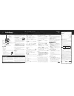
Contents

UHF Band

Service Manual

VX-450 Series

Vertex Standard LMR, Inc.

©2015 Vertex Standard LMR, Inc.

EC094U90Q

16 K

EY

 T

YPE

4 K

EY

 T

YPE

N

ON

 K

EY

 T

YPE

Summary of Contents for VX-450 series

Page 1: ...lignment Mode menu While we believe the information in this manual to be correct VERTEX STANDARD assumes no liability for damage that may occur as a result of typographical or other errors that may be present Your cooperation in pointing out any inconsis tencies in the technical information would be appreciated Important Note This transceiver is assembled using Pb lead free solder based on the RoH...

Page 2: ... 4 3 x 2 3 x 1 5 inches 109 x 58 5 x 37 mm VX 454 459 with FNB V133LI UNI 4 3 x 2 3 x 1 8 inches 109 x 58 5 x 45 mm VX 454 459 with FNB V134LI UNI Weight Approx 10 4 oz 296 g VX 451 with FNB V112LI Antenna Belt Clip 12 0 oz 340 g VX 451 with FNB V113LI Antenna Belt Clip 9 9 oz 281 g VX 451 with FNB V133LI UNI Antenna Belt Clip 11 6 oz 330 g VX 451 with FNB V134LI UNI Antenna Belt Clip 11 4 oz 322 ...

Page 3: ...rox 296 g VX 451 with FNB V112LI Antenna Belt Clip 340 g VX 451 with FNB V113LI Antenna Belt Clip 322 g VX 454 459 with FNB V112LI Antenna Belt Clip 366 g VX 454 459 with FNB V113LI Antenna Belt Clip 281 g VX 451 with FNB V133LI UNI Antenna Belt Clip 330 g VX 451 with FNB V134LI UNI Antenna Belt Clip 307 g VX 454 459 with FNB V133LI UNI Antenna Belt Clip 356 g VX 454 459 with FNB V134LI UNI Antenn...

Page 4: ...lable only as part of a desig nated assembly SP Connector Mating Operation 1 Insert the cable side first 2 Press down at the lever side NOTE Horizontal mating could damage the connector SP Connector Unmating Operation 1 Hook the lever 2 Pull up friction lock is released 3 Positive lock is released and removal completes Friction lock Positive lock Please remove the speaker connector from DISPLAY Un...

Page 5: ...Insert the cable side first 2 Press down at the lever side NOTE Horizontal mating could damage the connector SP Connector Unmating Operation 1 Hook the lever 2 Pull up friction lock is released 3 Positive lock is released and removal completes Friction lock Positive lock Please remove the speaker connector from DISPLAY Unit when you remove a FRONT Case of the transceiver RA1405100 O RING CAP RA140...

Page 6: ...ERSION K 16 KEY 4 KEY CP9819008 VERSION D NON KEY CP9819009 VERSION A NON KEY CP9819010 VERSION I NON KEY CP9819011 VERSION K NON KEY MIC SP CAP ASSY CB6642000 KNOB VOL RA125100B 1 KNOB FREQ RA125110B 1 HOLDER LCD RA1243200 16 KEY 4 KEY 1 LIGHT GUIDE LCD RA1243300 16 KEY 4 KEY 1 INTER CONNECTOR RA124340A 16 KEY 4 KEY 1 SPONGE RUBBER LCD RA1243500 16 KEY 4 KEY 1 REFLECTOR SHEET RA1243700 16 KEY 4 K...

Page 7: ... XTAL FILTER MFT67P 67 650MHZ H1102471 1 B d3 MAIN 2 UNIT VERSION I K CD3001 CERAMIC DISC ECDA450C24 H7901460 1 B c3 CF3001 CERAMIC FILTER LTWC450F H3900563 1 B a3 CF3002 CERAMIC FILTER LTWC450H H3900584 1 B b3 F 3001 CHIP FUSE 3 15A FHC16 322ADTP Q0000118 1 A B2 J 3008 CONNECTOR DF57H 2P 1 2V 21 P0091595 NON KEY 1 A B1 MC3001 MIC ELEMENT PF0 1055P M3290045 NON KEY 1 A C1 Q 3006 FET RQA0011DNS G0 ...

Page 8: ...8 VX 450 Series UHF Band Service Manual Block Diagram Version A D 16 key 4 key Type RF Section ...

Page 9: ...9 VX 450 Series UHF Band Service Manual Block Diagram Version A D 16 key 4 key Type Frequency Generation Reguration Section ...

Page 10: ...10 VX 450 Series UHF Band Service Manual Block Diagram Version A D 16 key 4 key Type AF Section ...

Page 11: ...11 VX 450 Series UHF Band Service Manual Block Diagram Version A D 16 key 4 key Type Controller Section ...

Page 12: ...12 VX 450 Series UHF Band Service Manual Block Diagram Version A D Non key Type RF Section ...

Page 13: ...13 VX 450 Series UHF Band Service Manual Block Diagram Version A D Non key Type Frequency Generation Reguration Section ...

Page 14: ...14 VX 450 Series UHF Band Service Manual Block Diagram Version A D Non key Type AF Section ...

Page 15: ...15 VX 450 Series UHF Band Service Manual Block Diagram Version A D Non key Type Controller Section ...

Page 16: ...16 VX 450 Series UHF Band Service Manual Block Diagram Version I K 16 key 4 key Type RF Section ...

Page 17: ...17 VX 450 Series UHF Band Service Manual Block Diagram Version I K 16 key 4 key Type Frequency Generation Reguration Section ...

Page 18: ...18 VX 450 Series UHF Band Service Manual Block Diagram Version I K 16 key 4 key Type AF Section ...

Page 19: ...19 VX 450 Series UHF Band Service Manual Block Diagram Version I K 16 key 4 key Type Controller Section ...

Page 20: ...20 VX 450 Series UHF Band Service Manual Block Diagram Version I K Non key Type RF Section ...

Page 21: ...21 VX 450 Series UHF Band Service Manual Block Diagram Version I K Non key Type Frequency Generation Reguration Section ...

Page 22: ...22 VX 450 Series UHF Band Service Manual Block Diagram Version I K Non key Type AF Section ...

Page 23: ...23 VX 450 Series UHF Band Service Manual Block Diagram Version I K Non key Type Controller Section ...

Page 24: ...ns the second mixer second local oscillator limiter ampli fier noise amplifier and RSSI amplifier The signal from reference oscillator X1001 becomes 4 times of frequencies in Q1033 it is mixed with the IF signal and becomes 450 kHz The second IF then passes through the ceramic filter CF1001 or CF1002 to strip away unwanted mixer products and is applied to the limiter amplifier in Q1033 which remov...

Page 25: ...cy as the output of reference divider These two signals are compared by phase detector the phase difference pulse is gen erated Circuit Description Version A D 2 5 2 Carrier Squelch The CPU 14 pin A D port detect RSSI voltage out put from Q1033 12 pin and controls AF output The RSSI output voltage changes according to the signal strength of carrier The stronger signal makes the RSSI voltage to be ...

Page 26: ...locked by the control of this DC voltage The PLL serial data from CPU is sent with three lines of SDO 40 pin SCK 36 pin and PSTB 30 pin The lock condition of PLL is output from the UL 18 pin terminal and UL becomes H at the time of the lock condition and becomes L at the time of the unlocked condition The CPU always watches over the UL condition and when it becomes L unlocked condition the CPU pro...

Page 27: ...econd mixer second local oscillator limiter ampli fier noise amplifier and RSSI amplifier Circuit Description Version I K The signal from reference oscillator X3001 becomes 4 times of frequencies in Q3033 it is mixed with the IF signal and becomes 450 kHz The second IF then passes through the ceramic filter CF3001 or CF3002 to strip away unwanted mixer products and is applied to the limiter amplif...

Page 28: ... detector Q3040 1 NJM12904V detects the current of Q3006 and Q3008 and converts the current difference to the voltage difference The output from the current detector Q3040 1 is com pared with the reference voltage and amplified by the power control amplifier Q3040 2 The output from Q3040 2 controls the gate bias of the final amplifiers Q3006 and the final amplifier driver Q3008 The reference volta...

Page 29: ...etector the phase difference pulse is gen erated The phase difference pulse and the pulse from through the charge pumps and LPF It becomes the DC voltage to control the VCO The oscillation frequency of VCO is locked by the control of this DC voltage The PLL serial data from CPU is sent with three lines of SDO 40 pin SCK 36 pin and PSTB 30 pin The lock condition of PLL is output from the UL 18 pin ...

Page 30: ...dard reserves the right to change circuits and alignment procedures in the interest of improved performance without notifying owners Under no circumstances should any alignment be attempted unless the normal function and operation of the transceiver are clearly understood the cause of the malfunction has been clearly pinpointed and any faulty components replaced and realignment determined to be ab...

Page 31: ...gnments should be made with oscillator shields and circuit boards firmly affixed in place Also the test equipment must be thoroughly warmed up before beginning Note Signal levels in dB referred to in the alignment procedure are based on 0 dBμ EMF 1 μV Test Setup Setup the test equipment as shown below for trans ceiver alignment apply 7 5 V DC power to the trans ceiver The Alignment Tool Outline In...

Page 32: ...lch SQL RSSI 5 TX Power High Low3 Low2 Low1 6 Maximum Deviation Wide Narrow Please adjust the following items when needed Modulation Balance Wide Narrow CTCSS Deviation Wide Narrow DCS Deviation Wide Narrow DTMF Alignment Seq Tone VOX ON Level TX MSK LTR Deviation Battery To enter the Alignment Mode select Alignment in the main Radio menu It will start to Upload the alignment data from the radio t...

Page 33: ...gn ment The Frequency Alignment window will appear 2 Click the PTT button or press the SPACE bar and the radio will start to transmit on the center frequency channel 3 Set the value to get the desired frequency by drag ging the slide bar clicking the up down button pressing the left or right arrow key or entering the value in the entry box 4 After getting the desired frequency click the PTT button...

Page 34: ... Up Down arrow key to switch to the se lected channel 3 Set the Signal Generator according to the indica tion at the top of the screen Setting Your SG as followings 4 Drag the slide bar click the up down buttons press the left or right arrow key or enter the value in the entry box to get the best RX sensitivity Highest RSSI value 5 Click the OK button to finish the RX Sensitivity alignment and sav...

Page 35: ...he Alignment for the level 15 of the RSSI SQL level at Wide 5k 4k or Narrow 2 5k TX Save RSSI Level TX SAVE W N The Alignment for the TX Save RSSI level at Wide 5k 4k or Narrow 2 5k The procedure for all the alignments is as follows 1 Click the Start button to open the alignment window in the SQL RSSI Alignment menu 2 The Alignment window will appear Set the Sig nal Generator according to the indi...

Page 36: ...transmit on the selected channel 4 Set the value to get desired output power High 5 W Low3 2 5 W Low2 1 W Low1 250 mW on the Power Meter by dragging the slide bar click ing the up down button pressing the left or right arrow key or entering the value in the entry box on the selected channel 5 After getting the desired output power click the PTT button or press the SPACE bar to stop transmitting 6 ...

Page 37: ...he de sired channel 5 Click the PTT button or press the SPACE bar the radio starts to transmit on the selected chan nel 6 Set the value to get desired deviation Wide 4 2kHz Narrow 2 1kHz on the deviation meter by dragging the slide bar clicking the up down button pressing the left or right arrow key or entering the value in the entry box on the selected channel 7 After getting the desired deviatio...

Page 38: ...e bar or press the Up Down arrow key to select the de sired channel 5 Click the PTT button or press the SPACE bar the radio starts to transmit on the selected chan nel 6 Set the value to get the best square wave on the Oscilloscope by dragging the slide bar clicking the up down button pressing the left or right ar row key or entering the value in the entry box on the selected channel 7 After getti...

Page 39: ...n the selected channel 4 Set the value to get desired deviation on the de viation meter by dragging the slide bar clicking the up down button pressing the left or right ar row key or entering the value in the entry box on the selected channel 5 After getting the desired deviation Wide 0 6 kHz Narrow 0 3 kHz click the PTT button or press SPACE bar to stop transmitting 6 Click the OK button to finis...

Page 40: ...on the selected channel 4 Set the value to get desired deviation Wide 0 6 kHz Narrow 0 3 kHz on the deviation meter by dragging the slide bar clicking the up down button pressing the left or right arrow key or entering the value in the entry box on the selected channel 5 After getting the desired deviation click PTT button or press SPACE bar to stop transmitting 6 Click the OK button to finish the...

Page 41: ...top trans mitting 5 Click the OK button to finish the DTMF Devia tion alignment and save the data SEQUENTIAL TONE DEVIATION This parameter is to align Sequential Tone Deviation 1 Press the Seq Tone button to start the alignment The Sequential Tone Deviation Alignment win dow will appear 2 Click the PTT button or press the SPACE bar the radio starts to transmit on the Center fre quency channel 3 Se...

Page 42: ...nment value in the New box Default 80 Input Range 0 Level Down 255 Level Up 3 Click the OK button the data will be saved and the alignment is complete TX MSK LEVEL This parameter is to align the modulation level of the ANI function 1 Press the TX MSK button to start the alignment The TX MSK Level window will appear 2 Then input the alignment value in the New box Default 9 Input Range 0 Level Down ...

Page 43: ...ick the OK button the data will be saved and the alignment is complete 4 Set the value of the DC Power source to 7 5V ac cording to the indication LTR DEVIATION This parameter is to align the LTR Deviation This parameter does not appear when adjusting the transceiver which is not installed the LTR feature 1 Press the LTR Dev button to start the alignment The LTR Deviation window will appear 2 Then...

Page 44: ...44 VX 450 Series UHF Band Service Manual MAIN Unit Circuit Diagram Version A D 16 key 4 key Type Lot 1 4 ...

Page 45: ...45 VX 450 Series UHF Band Service Manual MAIN Unit Parts Layout Version A D 16 key 4 key Type Lot 1 4 Side A 1 3 2 4 A B C D E F G ...

Page 46: ...46 VX 450 Series UHF Band Service Manual MAIN Unit Parts Layout Version A D 16 key 4 key Type Lot 1 4 Side B a b c d e f g 1 3 2 4 ...

Page 47: ...47 VX 450 Series UHF Band Service Manual MAIN Unit Circuit Diagram Version A D 16 key 4 key Type Lot 5 6 ...

Page 48: ...48 VX 450 Series UHF Band Service Manual MAIN Unit Parts Layout Version A D 16 key 4 key Type Lot 5 6 Side A 1 3 2 4 A B C D E F G ...

Page 49: ...49 VX 450 Series UHF Band Service Manual MAIN Unit Parts Layout Version A D 16 key 4 key Type Lot 5 6 Side B a b c d e f g 1 3 2 4 ...

Page 50: ...50 VX 450 Series UHF Band Service Manual MAIN Unit Circuit Diagram Version A D 16 key 4 key Type Lot 7 ...

Page 51: ...51 VX 450 Series UHF Band Service Manual MAIN Unit Parts Layout Version A D 16 key 4 key Type Lot 7 Side A 1 3 2 4 A B C D E F G ...

Page 52: ...52 VX 450 Series UHF Band Service Manual MAIN Unit Parts Layout Version A D 16 key 4 key Type Lot 7 Side B a b c d e f g 1 3 2 4 ...

Page 53: ...53 VX 450 Series UHF Band Service Manual MAIN Unit Circuit Diagram Version A D Non key Type Lot 1 7 ...

Page 54: ...54 VX 450 Series UHF Band Service Manual MAIN Unit Parts Layout Version A D Non key Type Lot 1 7 Side A 1 3 2 4 A B C D E F G ...

Page 55: ...55 VX 450 Series UHF Band Service Manual MAIN Unit Parts Layout Version A D Non key Type Lot 1 7 Side B a b c d e f g 1 3 2 4 ...

Page 56: ...56 VX 450 Series UHF Band Service Manual MAIN Unit Circuit Diagram Version A D Non key Type Lot 8 ...

Page 57: ...57 VX 450 Series UHF Band Service Manual MAIN Unit Parts Layout Version A D Non key Type Lot 8 Side A 1 3 2 4 A B C D E F G ...

Page 58: ...58 VX 450 Series UHF Band Service Manual MAIN Unit Parts Layout Version A D Non key Type Lot 8 Side B a b c d e f g 1 3 2 4 ...

Page 59: ...59 VX 450 Series UHF Band I Band Service Manual MAIN 2 Unit Circuit Diagram Version I K 16 key 4 key Type ...

Page 60: ...60 VX 450 Series UHF Band I Band Service Manual MAIN 2 Unit Parts Layout Version I K 16 key 4 key Type Side A A B C D E F G 1 3 2 4 ...

Page 61: ...61 VX 450 Series UHF Band I Band Service Manual a b MAIN 2 Unit Parts Layout Version I K 16 key 4 key Type Side B c d e f g 1 3 2 4 ...

Page 62: ...62 VX 450 Series UHF Band I Band Service Manual MAIN 2 Unit Circuit Diagram Version I K Non key Type ...

Page 63: ...63 VX 450 Series UHF Band I Band Service Manual MAIN 2 Unit Parts Layout Version I K Non key Type Side A A B C D E F G 1 3 2 4 ...

Page 64: ...64 VX 450 Series UHF Band I Band Service Manual a b Side B c d e f g 1 3 2 4 MAIN 2 Unit Parts Layout Version I K Non key Type ...

Page 65: ...65 VX 450 Series UHF Band Service Manual DISPLAY Unit Circuit Diagram 16 key 4 key Type Lot 1 4 ...

Page 66: ...66 VX 450 Series UHF Band Service Manual DISPLAY Unit Parts Layout 16 key 4 key Type Lot 1 4 Side A A B C D E 1 3 2 4 ...

Page 67: ...67 VX 450 Series UHF Band Service Manual DISPLAY Unit Parts Layout 16 key 4 key Type Lot 1 4 Side B a b c d e 1 3 2 4 ...

Page 68: ...68 VX 450 Series UHF Band Service Manual DISPLAY Unit Circuit Diagram 16 key 4 key Type Lot 5 Circuit Diagram ...

Page 69: ...69 VX 450 Series UHF Band Service Manual DISPLAY Unit Parts Layout 16 key 4 key Type Lot 5 Side A A B C D E 1 3 2 4 ...

Page 70: ...70 VX 450 Series UHF Band Service Manual DISPLAY Unit Parts Layout 16 key 4 key Type Lot 5 Side B a b c d e 1 3 2 4 ...

Page 71: ...f this manual may be reproduced without the permission of Vertex Standard LMR Inc Vertex Standard is a trademark of Vertex Standard LMR Inc All other trademarks are the property of their respective owners 2015 Vertex Standard LMR Inc All rights reserved ...

Reviews: