background image

3

 Alignment instruction


3.1 Debugging item 

a)adjust mode instruction 
b)B+ voltage adjustment 
c)RFAGC voltage adjustment 
d)focus adjustment 
e)Screen-grid voltage white balance, sub brightness adjustment 
f)filed scan center, line , amplitude adjustment 
g)H-scan center adjustment 

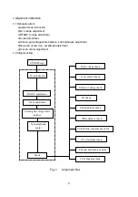
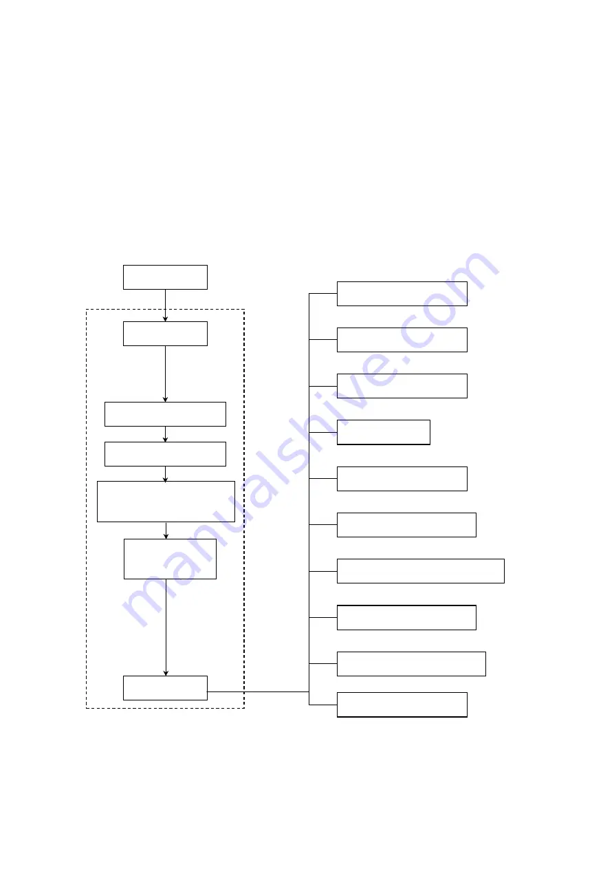
3.2 Alignment flow


Fig-1    alignment flow 

E

2

PROM copy 

B+ adjustment 

RFAGC adjustment 

Focus adjustment 

Screen-grid voltage white 

balance 

Scan amplitude 

center 

check 

The unit and remote control 

AV, S terminal check 

Color Purity, convergence check 

White balance check 

Sub brightness check 

AV check 

Filament voltage check 

X-ray protect check 

High voltage check 

CCD function check 

Summary of Contents for TK2016

Page 1: ...COLOR TELEVISION TK2026 TK2016...

Page 2: ...CONTENTS Safety instruction 1 General instruction 1 Alignment instruction 2 Alignment flow 2 Alignment method 3 Block diagram 10 MAIN IC 11 Schematic diagram 16 APPENDIX Exploded view Part list...

Page 3: ...is have special safety related characteristics These characteristics are often passed unnoticed by a visual inspection Replacement parts which have these special safety characteristics are identified...

Page 4: ...ine amplitude adjustment g H scan center adjustment 3 2 Alignment flow Fig 1 alignment flow E2 PROM copy B adjustment RFAGC adjustment Focus adjustment Screen grid voltage white balance Scan amplitude...

Page 5: ...the negative pole of VD524 b receive PHILIPS test pattern signal and set the picture to standard c Adjust VR501 to let the value of B voltage be 110 V 0 5 V yongxin super pure flat 4 2 AGC adjustment...

Page 6: ...of test pattern above blanking d select V SHIFT menu and adjust to let the vertical center of picture coincide with vertical center of picture tube e Select V SIZE menu and adjust to let the vertical...

Page 7: ...without raster without sound Disconnect the DC regulated voltage power picture and sound should restore to normal 4 12 4 Picture and sound check 1 Receive standard TV signal 2 Use picture control butt...

Page 8: ...ime to let the red and blue horizontal lines coincide at middle of screen f Adjust two hexode magnetic rings to let the green line coincide with the mixed line of red and blue Adjust the angle between...

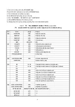
Page 9: ...ON M1 V SLOPE 0 63 36 field center adjustment V SHIFT 0 63 32 field point adjustment V SIZE 0 63 36 field amplitude adjustment V SC 0 63 32 field line HSHIFT 0 63 32 line point adjustment PROGRAMA NO...

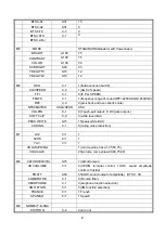
Page 10: ...N 0 1 0 1 push pull output 0 OC gate output SOFT CLIP 0 3 3 white level limit PEAK WHITE 0 15 15 peak white limit CORING 0 1 0 coring noise reduction M7 AV2 0 1 1 SVHS 0 1 1 YUV 0 1 1 VOLADJPOING 1 vo...

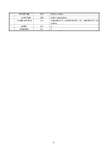
Page 11: ...9 STARTTIME 6 15 8 turn on time IF OFFSET 0 63 32 IF compensate TUNER OPTION 0 2 0 BXATB011F X BXATB108F K 1 BXATB017F K 2 XXX GAME 0 1 0 GALENDA 0 1 0...

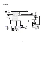
Page 12: ...IO OUT IK RGB OUT V OUT H OUT S TRAP Vo V2i V1i Y Cr Cb ARi2 ARi1 ALi2 ALi1 S VHS 24C08 KA5Q0765 T501 POWER UNIT 110V 26V 12V 8V 5V 3 3V CRT BOARD V IN STV9302A V OUT H IN H OUT TT2140 T451 H OUT DY 1...

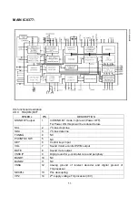
Page 13: ...I2 C bus clock line SDA 3 I2 C bus data line TUNING 4 NC P3 0 NTSC SW 5 NC KEY 6 Control keys input VOL 7 Sound Volume control PWM output MUTE 8 Sound mute output VSSC P 9 Digit ground for controller...

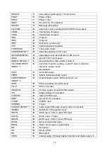
Page 14: ...ling sound IF input subcarrier reference output audio deemphasis HOUT 33 horizontal output FBISO 34 flyback input sandcastle output AUDEXT QSSO AMOUT 1 35 external audio output QSS intercarrier out EH...

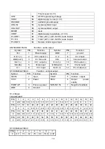
Page 15: ...Mute input GND out 2 11 Ch 2 Ground In 1 6 Ch 1 input Out 2 12 Ch 2 output STV9302A LA78040 Function vertical output Symbol PIN Function Symbol PIN Function INV IN 1 Input V OUT 5 Vertical output VCC1...

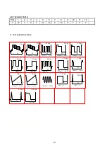
Page 16: ...5Vpp 0 9Vpp 920Vpp H H 1Vpp V H H CRT KB CRT KG CRT KR 95Vpp 95Vpp 95Vpp H H H T501 PIN7 300Vpp 22Vpp H H V451 B 2 7Vpp TDA8377 PIN53 2 5Vpp 2 5Vpp 3 8Vpp H H H TDA8377 PIN52 TDA8377 PIN51 TDA8377 PIN...

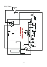
Page 17: ...15 Wiring diagram...

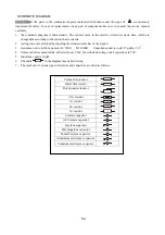
Page 18: ...ed 3 resistance unit is in Ohm namely K 1000 M 1000K Capacitance unit is in F P F 10 6 4 Unless othervise noted inside all resistors are 1 6W the withstand voltage of all capacitor are 50V 5 Inductanc...

Page 19: ......

Page 20: ...1 2 3 4 5 6 7 8 9 10 11 12 13 14 15 16 17 18 19 20 21 22 23 24 25...

Page 21: ...SWITCH KFC A06 4X4 5X5B 360 10001 00 12 BUTTON BOARD ASSY 667 TK2026 05 13 BUTTON 877 60546 00 14 LED COLUMN 700 60156 00 15 FRONT CABINET 611 30358J0H1 16 LEFT LEAD TRACK RIGHT LEAD TRACK 870 20845 2...

Page 22: ...RE SPRING 851 24016 14 SCREW SJ2824 ST4X16C Y 851 24020 14 SCREW SJ2824 ST4X20C Y 851 24020 14 SCREW SJ2824 ST4X20C Y 851 53010 11 SCREW SJ2825 ST3X10C D Zn 851 53010 31 SCREW SJ2825 ST3X10FT D Zn 851...

Page 23: ...2016 PRIMA 615 20100 00 SPEAKER ASS Y 384 40908 U0 SPEAKER ST512 02 655 61201 154 6 PINS LEAD WITH HOUSING 851 53010 31 SCREW SJ2825 ST3X10FT D Zn 868 20217 00 WASHER 870 20854 00 SPEAKER BRACKET 667...

Page 24: ...1 4W 1 8K G R405 467 2E210 H0 METAL RESISTOR 1 2W 1k JL R460 467 8E522 H0U SOLID RESISTOR 1 2W 2 2M JL R588 471 2001K 00 PEAKING COIL SPT0305 1R0K 5 L302 475 25451 00 CERAMIC TRAP FILTER XT4 5MB Z351...

Page 25: ...CC1 12 SL 63V 471J C812 459 2147H 902 CERAMIC CAPACITOR CC1 12 SL 63V 471J C814 459 2147H 902 CERAMIC CAPACITOR CC1 12 SL 63V 471J C824 459 2147H 902 CERAMIC CAPACITOR CC1 12 SL 63V 471J C826 459 215...

Page 26: ...10uF M C367 464 6D610 M02 ELECTROLYTIC CAPACITOR CD110 16V 10uF M C807 464 6D622 M02 ELECTROLYTIC CAPACITOR CD110 16V 22uF M C745 464 6D622 M02 ELECTROLYTIC CAPACITOR CD110 16V 22uF M C352 464 6D647...

Page 27: ...50V 22uF M C703 464 60647 M02 ELECTROLYTIC CAPACITOR CD110 50V 47uF M C462 464 60647 M02 ELECTROLYTIC CAPACITOR CD110 50V 47uF M C517 464 62547 M02 ELECTROLYTIC CAPACITOR CD288 160V 4 7uF M C466 467...

Page 28: ...1 6W 300 J R933 467 1C133 H03 CARBON RESISTOR 1 6W 330 J R916 467 1C133 H03 CARBON RESISTOR 1 6W 330 J R926 467 1C133 H03 CARBON RESISTOR 1 6W 330 J R936 467 1C139 H03 CARBON RESISTOR 1 6W 390 J R322...

Page 29: ...J R321 467 1C247 H03 CARBON RESISTOR 1 6W 4 7K J R131 467 1C247 H03 CARBON RESISTOR 1 6W 4 7K J R133 467 1C247 H03 CARBON RESISTOR 1 6W 4 7K J R154 467 1C247 H03 CARBON RESISTOR 1 6W 4 7K J R158 467 1...

Page 30: ...ISTOR 1 6W 47K J R745 467 1C347 H03 CARBON RESISTOR 1 6W 47K J R807 467 1C368 H03 CARBON RESISTOR 1 6W 68K J R173 467 1C410 H03 CARBON RESISTOR 1 6W 100K J R483 467 1C410 H03 CARBON RESISTOR 1 6W 100K...

Page 31: ...3 COPPER M11 895 6016030 50 RIVET GB876 86 1 6X3 COPPER M12 895 6016030 50 RIVET GB876 86 1 6X3 COPPER M13 895 6016030 50 RIVET GB876 86 1 6X3 COPPER M14 895 6016030 50 RIVET GB876 86 1 6X3 COPPER M15...

Page 32: ...UMPER WIRE W271 998 JUMPER WIRE W312 998 JUMPER WIRE W313 998 JUMPER WIRE W331 998 JUMPER WIRE W341 998 JUMPER WIRE W342 998 JUMPER WIRE W343 998 JUMPER WIRE W344 998 JUMPER WIRE W352 998 JUMPER WIRE...

Page 33: ...UMPER WIRE W562 998 JUMPER WIRE W563 998 JUMPER WIRE W571 998 JUMPER WIRE W581 998 JUMPER WIRE W591 998 JUMPER WIRE W621 998 JUMPER WIRE W622 998 JUMPER WIRE W642 998 JUMPER WIRE W643 998 JUMPER WIRE...

Page 34: ...JUMPER WIRE R520 998 JUMPER WIRE R581 998 JUMPER WIRE R551 895 6016030 50 RIVET GB876 86 1 6X3 COPPER M29 998 JUMPER WIRE W262 998 JUMPER WIRE W267 667 TK2026 05 KEY BOARD ASS Y 340 10055 90 LED HFT5...

Page 35: ...WHITE 03 667 TK2150 29B SIDE AV BOARD ASS Y 364 11205 00 EARPHONE JACK 3F27K XV05 364 36101 00 6 PINS CONNECTORS TJC3 06A XV04 364 93202 00 AV JACK AV306 2 XA01 464 6D647 M0 ELECTROLYTIC CAPACITOR CD...

Reviews: