background image

Working principle analysis of the unit 

1.  Starting of the system 
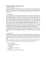
The system adopts 264MHz, 32bit MIPS CPU of Linux operating system. It needs bootstrap routine 
to start the unit after power-on, which stored in N142 (serial Flash in the block diagram). After 
bootstrap routine finish, start the Linux operating system and application programs from N141 
(Nand Flash). 
 
2.  Video signal flow 
Antenna reception signal send to digital-analog integrative tuner (contain HF and IF amplifier circuit), 
which integrate decoder for analog NTSC, direct output NTSC composite video signal, and 
integrate digital IF amplifier circuit. The tuner is controlled by the command (SDA and SCL) of N1 
(X240H), select appropriate channel to store the signal into X240H. For the channel resource is 
fixed, it can’t transmit the analog and digital program at the same time, X240 reception signal from 
the tuner is analog CVBS (NTSC program) or the digital differential IF signal (ATSC/Clear QAM 
program), only one of them. The digital IF signal is demodulated and MPEG decoded in X240.   
AV and S-video signal via matched component direct send to N1 (X240H) video switch, A/D 
conversion and digital decode; YPbPr via matched component send to video switcher 
N701(PI5V330Q), the selected signal and D-Sub signal send to N502 (AD9880) ADC, then output 
24bit RGB/YCbCr 4:2:2 to N1; HDMI also via N502 (AD9880) output 24bit YCbCr 4:2:2 to N1. 
The all video signals (contain DTV video) send to X240H image scale and OSD superposition, then 
output RGB signal of 24bit to LVDS switcher N561 (THC63LVDM83R), in there the signal is 
converted into 3 pairs low voltage differential signals and 1 pair clock signal, then send to LCD 
panel. 
 
3.  Audio signal flow 
Sound signal (SIF, AV sound, YPbPr and D-Sub) via NB04 HEF4052BT (sound diverter switch) to 
output signal, it send to N201 (MPS4440G on 53# board) sound processing and switch of audio, 
select I2S digital audio signal, send to X240H video-sound synchronization, then send back to N201. 
Likewise, I2S audio signal of HDMI send to X240H video-sound synchronization, then send back to 
N201.  
At last, sound signal send to N201 D/A convert and process of sound effect. Select left/right audio 
channel, their send to sound amplifier NV01 (TPA3008) amplify, then send to speaker. 
 
4.  Function of ATMEGA 8 

a.  key scan and infrared control   
b. power on/off 
c. VGA 

control  

d.  Brightness control of backlight   
e. Timing  
N801 communicates with N1 (X240) by UART 


Summary of Contents for LC-32FC18

Page 1: ...LCD TELEVISION LC 32FC18 America ...

Page 2: ...cautions Alignment instructions Working principle analysis of the unit Block diagram IC block diagram Wiring diagram Troubleshooting Schematic diagram APPENDIX A Assembly list APPENDIX B Exploded View 1 3 8 9 10 16 17 27 ...

Page 3: ... will result 2 5 If any foreign substance such as water liquid metal slices or other matters happens to fall into the module be sure to cut the power off immediately and do not move anything on the module lest it should cause fire or electric shock due to contact with the high voltage or short circuit 2 6 Should there be smoke abnormal smell or sound from the module please shut the power off at on...

Page 4: ...0 85 Scope for storage 10 90 2 13 Display of a fixed picture for a long time may result in appearance of picture residue on the screen as commonly called ghost shadow The extent of the residual picture varies with the maker of LCD screen This phenomenon doesn t represent failure This ghost shadow may remain in the picture for a period of time several minutes But when operating it please avoid disp...

Page 5: ...re and sound are normal Analog board power test Check accessories and then packing Input YPbPr YcbCr 1 2 signal and check if picture sound and analog quantity control is normal in the state of COMPONENT FLASH write N501 N142 N710 N801 Digital board power test Test of Button board and IR board Aging ADC emendation and white balance adjustment Connect to central signal source check various TV functi...

Page 6: ...k 4 2 Adjustment of unit connection Turn on the TV and check if it is normal display LOGO about 2 seconds later display picture about 10 seconds later 4 3 Aging a Turn on the TV select TV channel without signal input b Aging for an hour in the aging room 4 4 White balance adjustment of ACD use CA210 VG849 generator Enter MENU Picture Picture Settings set Preset to standard Note 1 Press and to swit...

Page 7: ... to the central signal source Enter the channels menu scan channels select input type Antenna to auto search and check if there is station skipping Check if search Find channel the output of earphone and speakers and the picture are normal 5 2 AV S Video terminal Connect AV S Video signal check if they are normal 5 3 YPBPR terminal Input YUV signal VG 848 signal generator separate input the YUV fo...

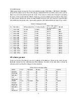
Page 8: ... 72 00 31 50 VESA 4 640 X 480 37 50 75 00 31 50 VESA 5 640 X 480 43 30 85 00 36 00 VESA 6 800 X 600 35 16 56 25 36 00 VESA 7 800 X 600 37 90 60 00 40 00 VESA 8 800 X 600 46 90 72 19 49 50 VESA 9 800 X 600 48 08 75 00 50 00 VESA 10 800 X 600 48 08 85 00 56 25 VESA 11 1024 X 768 48 40 60 00 65 00 VESA 12 1024 X 768 56 50 70 00 75 00 VESA 13 1024 X 768 60 00 75 00 78 75 VESA 6 Ex factory preset There...

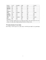
Page 9: ...rightness 20 25 20 30 25 Saturation 30 25 20 26 25 HDMI Vivid Standard Mild Pro Custom Tint 25 25 25 25 25 Sharpness 25 25 25 30 25 Note in the status of factory P2 it can change the settings of the preset picture and sound modes in the other status adjusted settings are stored in Custom mode 7 Preset ex factory of user menu Enter setting reset all press ok to select reset turn off the power after...

Page 10: ...1 X240H video switch A D conversion and digital decode YPbPr via matched component send to video switcher N701 PI5V330Q the selected signal and D Sub signal send to N502 AD9880 ADC then output 24bit RGB YCbCr 4 2 2 to N1 HDMI also via N502 AD9880 output 24bit YCbCr 4 2 2 to N1 The all video signals contain DTV video send to X240H image scale and OSD superposition then output RGB signal of 24bit to...

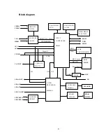
Page 11: ...owerControl SIF I2S I I2S UART KEY L R AVOUT IR L R AV1 L R AV2 L R VGA DVI L R YPbPr1 L R YPbPr2 HDTV SW PI5V330 RECEIVER AD9880 LCD TV CONTROLLER X240H AUDIO PROCESSOR MSP4440 AUDIO SW HEF4052 HP AMP NJW1109 AUDIO AMP TPA3008 HEAD PHONE NAND FLASH 16 32M DDR SDRAM 32 64 128M LCD PANEL SPEAKER VIDEO SW PI5V331 LVDS THC63LVDM83R Serial FLASH 512K MEGA8 ...

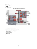
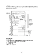
Page 12: ...diagram is below Function of X240H 1 Decoder of VSB QAM control of TUNER 2 264MHz 32bit MIPS CPU 3 MPEG decoder and format switch of HD and SD 4 NTSC Video Decoder with 3D Comb 5 USB 1 1 interface 6 Two I2S input output 7 S PDIF output ...

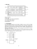
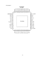
Page 13: ...tegrated on a single chip Also included is support for High bandwidth Digital Content Protection HDCP Main pins instruction 83 84 SCL SDA 49 50 DDCSCL DDCSDA connect with E2PROM store EDID and external HDMI 51 52 MCL MDA connect with E2PROM store HDCP KEY 66 71 77 R G B input for VGA 68 74 79 YPbPr input 90 PIXCLK 24 bit digital signal ...

Page 14: ...am A phase locked transmit clock is transmitted in parallel with the data streams over a fifth LVDS link At a transmit clock frequency of 85MHz 28bits of RGB data and 4bits of LCD timing and control data HSYNC VSYNC CNTL1 CNTL2 are transmitted at a rate of 595Mbps per LVDS channel Also available is THC63LVDM63R that converts 21bits of CMOS TTL data into LVDS Low Voltage Differential Signaling data...

Page 15: ...eliminates the need for external heatsinks when playing music The gain of the amplifier is controlled by two gain select pins The gain selections are 15 3 21 2 27 2 and 31 8 dB The outputs are fully protected against shorts to GND VCC and output output shorts A fault terminal allows short circuit fault reporting and automatic recovery Thermal protection ensures that the maximum junction temperatur...

Page 16: ...14 Block diagram of TPA3008D2 ...

Page 17: ...15 Pin description ...

Page 18: ...alog board 667 L32FC18 53 667 L32FC18 46 LVDS To backlight board To key board IR board Power board X711 X704 X702 X701 X703 X705 X301 X201 X804 X202 X801 X803 X804 X501 X561 X801 X802 X709 X271 XV01 XV02 X250 X102 X101 X100 X5 Wiring diagram 16 ...

Page 19: ...nd if interfered possibly by the equipment like transmitting antenna non professional radio station and cellular phone 1 2 TV set Symptoms Possible cause Unable to switch the power on Check to see if the power plug has been inserted properly into the socket No picture and sound Check to see if the power supply of liquid crystal TV has been switched on As can be indicated by the red LED at the fron...

Page 20: ... batteries are installed in the reverse order Check if the battery is effective Check the distance or angle from the monitor Check if there is any obstruct between the remote control and the TV set Check if the remote control signal receiving window is exposed to strong fluorescence No picture and sound but only hash Check if the antenna cable is correctly connected or if it has received the video...

Page 21: ...mm 10mm 5mm Total defected point 8 7 5 4 Notes 1 Definition of defected point bright spot dark spot It is identified as a defected point if its area exceeds 1 2 of a single picture element R G B 2 Definition of bright spot It is identified as a bright spot if it is bright in the state of dark field and its bright size remains unchanged 3 Definition of dark spot It is identified as a dark spot if i...

Page 22: ...ight board DDR N141 N142 G601 and the voltages Check if the display of each channel s video signal is normal Check if the signal inputted from the channel to pin IC is normal or IC and its periphery is normal or the output of LVDS is normal Check if the display of each channel s audio signal is normal Check if the signal inputted from the channel to pin IC is normal or IC N601 TPA3008D2 MSP4440 an...

Page 23: ...easure Standby5V Check if L508 is rosin joint or short to the ground The power supply board fails to work properly Check DDR N141 N142 G601 and their voltage Check Z801 N801 and V582 Check the capacitor and resistor of N801 Check R748 is low level or not if FU801 is 5V Check DDR N141 N142 G601 and their voltages the soldering of N1 Check if R571 is square wave Check if N1 is rosin joint Check the ...

Page 24: ...ck N1 and its periphery Refer to 4 checking procedure Check backlight board R748 is low level or not Yes No Yes No Sound only with raster Check if the power supply of LVDS is normal or not Check the signal outputted from N1 to N561 is normal or not Check the signal outputted from N561 to 61 is normal or not Check the power supply and the periphery circuit of N1 Check pin 5 of N807 is low level or ...

Page 25: ...ndent pins of power amplifier have output Check periphery circuit of power amplifier s back level Check if there have signals inputted from R207 and R208 to power amplifier Check periphery circuit of power amplifier power supply circuit and circuit of pin MUTE Check if correspondent channels of N201 have input signal Check periphery circuit of N801 crystal oscillation and power supply circuit Foll...

Page 26: ...supply circuit There exits problems at the place from socket of AV terminal to C861 or C862 Check periphery circuit of V805 or V808 and power supply circuit Yes No Yes No Check if C439 has input signal Check if C854 has input signal Check periphery circuit of N101 crystal oscillation and power supply circuit Check periphery circuit of TUNER power supply circuit and bus line There exits problems at...

Page 27: ...oing Check if the input signal of YPbPr is normal Check periphery circuit of N502 and I2C bus of R606 R607 There is trouble at the path between VGA socket and N502 Yes No Check if the input signal of VGA is normal Check periphery circuit of N502 and I2C bus of R606 R607 There is trouble at the path between YPbPr socket and N502 then check N701 Yes No Check if the input signal of VGA is normal Chec...

Page 28: ...ly g HDMI with no sound Check if R509 and R510 output square wave and check if R505 has signal or not 3 5 Abnormal picture a A certain differential wire pair of LVDS of X561 RX0 RX1 RX2 RX3 is abnormal which may lead to lack of color or color splash b The digital signal of 24bit of N561 is rosin joint which may lead to lack of color or color splash ...

Page 29: ...CPU board ...

Page 30: ...CPU board ...

Page 31: ...CPU board ...

Page 32: ...CPU board ...

Page 33: ...CPU board ...

Page 34: ...CPU board ...

Page 35: ...CPU board ...

Page 36: ...CPU board ...

Page 37: ...CPU board ...

Page 38: ...CPU board ...

Page 39: ...AV trans connect board ...

Page 40: ...analog board ...

Page 41: ...32 power board 667 L32T18 20 ...

Page 42: ...ital processing board 667 L32FC18 69 N561 N502 N1 THC63LVDM83R 353 00830 10 AD9880KST 100 353 98800 20 X240H 353 02400 10 Trans connect board 667 L32FC18 46 Keypad board 667 27FC18 05 Indicator light board 667 L32W18 14A IR board 667 L32W18 09 Power supply board 667 L32T18 20 Remote control 301 D42FB6 06E RC D06 0E Panel 335 32017 00 V320B1 L04 ...

Page 43: ...APPENDIX Exploded view LC 32X18 ...

Page 44: ...connecting assy 12 870 10219 00 Mounting holder 13 808 10867 AF0 Rear cabinet USB 14 808 10865 AF0 Rear cabinet right 15 780 G18L1 AF1 Rear cabinet 16 808 10812 AF0 Power lead cover 17 615 20482 00 Bottom speaker assy 18 615 10578 00 Stand assy 19 808 10863 AF0 Speaker connecting cover 20 808 10866 AF0 Rear cabinet bottom 21 808 10864 AF0 Rear cabinet left 22 808 10859 AF0 decorate cover leftright...

Page 45: ...603 L32FC18 14 Ver 1 1 ...

Reviews: