


ZCU102 Evaluation Board User Guide
115
UG1182 (v1.2) March 20, 2017
Appendix B
Master Constraints File Listing
Overview
The master Xilinx design constraints (XDC) file template for the ZCU102 board provides for
designs targeting the ZCU102 evaluation board. Net names in the constraints listed
correlate with net names on the latest ZCU102 evaluation board schematic. Identify the
appropriate pins and replace the net names with net names in the user RTL. See the
Vivado
Design Suite User Guide: Using Constraints
(UG903)
for more information.
For detailed I/O standards information required for a particular interface, refer to the
constraint files generated by tools such as the memory interface generator (MIG) and base
system builder (BSB).
The FMC connectors J5 (HPC0) and J4 (HPC1) are connected to MPSoC banks powered by
the variable voltage VAJ_FMC. Because different FMC cards implement different circuitry,
the FMC bank I/O standards must be uniquely defined by each customer.
IMPORTANT:
The XDC file can be accessed on the Zynq Ult ZCU102 Development Kit website.
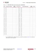
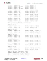
ZCU102 Board Constraints File Listing
#CLOCKS
#PS_REF_CLK 33 MHz U69 SI5341B
#Other net PACKAGE_PIN U24
- PS_REF_CLK Bank 503
#CLK_125 125 MHz U69 SI5341B
set_property PACKAGE_PIN F21 [get_ports "CLK_125_N"]
set_property IOSTANDARD LVDS_25
[get_ports "CLK_125_N"]
set_property PACKAGE_PIN G21
[get_ports "CLK_125_P"]
set_property IOSTANDARD LVDS_25
[get_ports "CLK_125_P"]
#CLK_74_25 74.25 MHz U69 SI5341B
set_property PACKAGE_PIN AK14
[get_ports "CLK_74_25_N"]
set_property IOSTANDARD LVDS_25
[get_ports "CLK_74_25_N"]
set_property PACKAGE_PIN AK15
[get_ports "CLK_74_25_P"]
set_property IOSTANDARD LVDS_25
[get_ports "CLK_74_25_P"]
#USER_SI570 300 MHz


