


ZC706 Evaluation Board User Guide
7
UG954 (v1.5) September 10, 2015
Chapter 1
ZC706 Evaluation Board Features
Overview
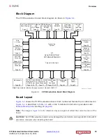
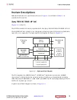
The ZC706 evaluation board for the XC7Z045 All Programmable SoC (AP SoC) provides a
hardware environment for developing and evaluating designs targeting the Zynq®-7000
XC7Z045-2FFG900C AP SoC. The ZC706 evaluation board provides features common to
many embedded processing systems, including DDR3 SODIMM and component memory, a
four-lane PCI Express® interface, an Ethernet PHY, general purpose I/O, and two UART
interfaces. Other features can be supported using VITA-57 FPGA mezzanine cards (FMC)
attached to the low pin count (LPC) FMC and high pin count (HPC) FMC connectors.
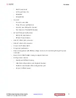
ZC706 Evaluation Board Features
The ZC706 evaluation board features are listed in here. Detailed information for each
feature is provided in
starting on
• Zynq-7000 XC7Z045-2FFG900C AP SoC
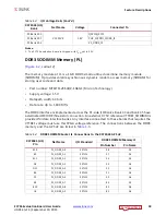
• 1 GB DDR3 memory SODIMM on the programmable logic (PL) side
• 1 GB DDR3 component memory (four [256 Mb x 8] devices) on the processing system
(PS) side
• Two 128 Mb Quad-SPI (QSPI) flash memory (Dual Quad-SPI)
• USB 2.0 ULPI (UTMI+ low pin interface) transceiver with micro-B USB connector
• Secure Digital (SD) connector
• USB JTAG interface via Digilent module with micro-B USB connector
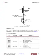
• Clock sources:
°
Fixed 200 MHz LVDS oscillator (differential)
°
I
2
C
programmable LVDS oscillator (differential)
°
Fixed 33.33 MHz LVCMOS oscillator (single-ended)
°
Subminiature version A (SMA) connectors (differential)
°
SMA connectors for GTX transceiver clocking (differential)