background image

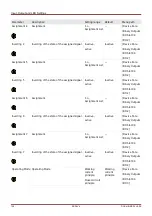
Input, Output and LED Settings

OR-4 X

BO Slot X5 ,BO Slot X6

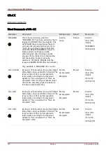
Direct Commands of OR- 4 X

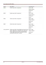
Parameter

Description

Setting range

Default

Menu path

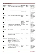
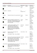
DISARMED

This is the second step, after the 
"DISARMED Ctrl" has been activated, that is 

required to DISARM the relay outputs. This 
will DISARM those output relays that are 

currently not latched and that are not on 
“hold” by a pending minimum hold time. 

CAUTION! RELAYS DISARMED in order to 
safely perform maintenance while 

eliminating the risk of taking an entire 
process off-line. (Note: Zone Interlocking 

and Supervision Contact cannot be 
disarmed). YOU MUST ENSURE that the 

relays are ARMED AGAIN after maintenance.

Only available if: DISARMED Ctrl = active

inactive, 

active

inactive

[Service

/Test (Prot 

inhibit)

/DISARMED

/BO Slot X5]

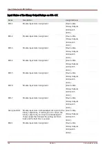
Force all Outs

By means of this function the normal Output 
Relay State can be overwritten (forced). The 

relay can be set from normal operation 
(relay works according to the assigned 

signals) to "force energized" or "force de-
energized" state. Forcing all outputs relays 

of an entire assembly group is superior to 
forcing a single output relay.

Normal, 

De-Energized, 

Energized

Normal

[Service

/Test (Prot 

inhibit)

/Force OR

/BO Slot X5]

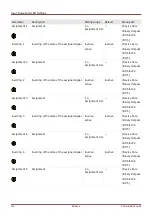
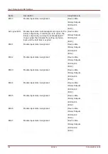
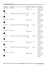
Force OR1

By means of this function the normal Output 

Relay State can be overwritten (forced). The 
relay can be set from normal operation 

(relay works according to the assigned 
signals) to "force energized" or "force de-

energized" state.

Normal, 

De-Energized, 

Energized

Normal

[Service

/Test (Prot 
inhibit)

/Force OR

/BO Slot X5]

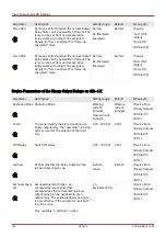
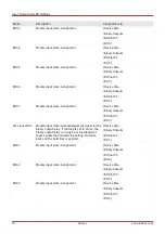
Force OR2

By means of this function the normal Output 
Relay State can be overwritten (forced). The 

relay can be set from normal operation 
(relay works according to the assigned 

signals) to "force energized" or "force de-
energized" state.

Normal, 

De-Energized, 

Energized

Normal

[Service

/Test (Prot 

inhibit)

/Force OR

/BO Slot X5]

153

MCDLV4

DOK-HB-MCDLV4-2E

Summary of Contents for HighPROtec MCDLV4

Page 1: ...Manual Line Differential Protection MCDLV4 Software Version 3 4 a DOK HB MCDLV4 2E Revision A English...

Page 2: ...urrent and Volt unbalance THD and THD Fund and RMS Max Min Avg phasors and angles Power Fund and RMS P Q S PF Metering Statistics and Demand Inrush 79 CTS 47 Standard 55 LOP 32 25 1 0 59N 59A 27A Prog...

Page 3: ...Order Code Order Code 3 MCDLV4 DOK HB MCDLV4 2E...

Page 4: ...0 RTU RS485 terminals B Modbus TCP DNP3 0 TCP UDP Ethernet 100 MB RJ45 C Profibus DP optic fiber ST connector D Profibus DP RS485 D SUB E Modbus RTU IEC60870 5 103 DNP3 0 RTU optic fiber ST connector...

Page 5: ...gic up to 80 equations The type of cards are as follows for the three main variants Variant Slot X1 Slot X2 Slot X3 Slot X4 Slot X5 Slot X6 MCDLV4 2 A DI8 X1 RO 6 X2 TI 4 TIS 4 cur transf TU volt tran...

Page 6: ...Slot X1 Power Supply Card with Digital Inputs 38 Slot X2 Relay Output Card 42 Slot X3 Current Transformer Measuring Inputs 45 Slot X4 Voltage Transformer Measuring Inputs 56 Slot X5 Multi Input Outpu...

Page 7: ...of the Demand Management 245 Signals of the Demand Management States of the Outputs 245 Global Protection Parameter of the Demand Management 246 States of the Inputs of the Demand Management 250 Ackno...

Page 8: ...Prot 479 Blocking all Protective Elements enduringly 479 Blocking all Protective Elements temporarily 479 Blocking all Trip Commands enduringly 480 Blocking all Trip Commands temporarily 480 General...

Page 9: ...Shedding 942 LVRT Low Voltage Ride Through 27 t 961 Intertripping Remote 977 PQS Power 32 37 985 PF Power Factor 55 1005 ExP External Protection 1014 Ext Temp Superv Protection Module External Tempera...

Page 10: ...with LC Connector for Long distance Protection Communication 1146 Boot phase 1148 Servicing and Maintenance 1149 Standards 1150 Approvals 1150 Design Standards 1150 High Voltage Tests 1151 EMC Immunit...

Page 11: ...Table of Contents md5_1 md5_2 RMS Handoff 0 File generated DOK HB MCDLV4 2E_A pdf This manual applies to devices version Version 3 4 a Build 35594 11 MCDLV4 DOK HB MCDLV4 2E...

Page 12: ...descriptions this manual includes Text graphic and formulae do not always apply to the actual delivery scope The drawings and graphics are not true to scale We do not accept any liability for damage a...

Page 13: ...th or serious injury WARNING indicates a hazardous situation which if not avoided could result in death or serious injury CAUTION used with the safety alert symbol indicates a hazardous situation whic...

Page 14: ...hat is to be protected You must ensure that the device will properly recognize and manage e g switch off the circuit breaker on the basis of your programming and parameterization all operational condi...

Page 15: ...ion of our website www woodward com If your publication is not there please contact your customer service representative to get the latest copy Important Information In line with the customer s requir...

Page 16: ...e work area as much as possible 4 Do not remove any printed circuit board PCB from the control cabinet unless absolutely necessary If you must remove the PCB from the control cabinet follow these prec...

Page 17: ...entation as well as the parameter setting and evaluation software Please check the consignment for completeness on arrival delivery note Please ascertain whether the type plate connection diagram type...

Page 18: ...pecially reserved for this purpose In general appropriate local guidelines and regulations must be followed when disposing of electrical devices and batteries Purpose of the Battery The purpose of the...

Page 19: ...a pre defined value can be selected 1 n Assignment List name 1 n VeEnable no assignment 1 n no assignm ent 1 name 1 n Assignment List Parameter of a Module Input with special values An 1 n output from...

Page 20: ...ll be reset by 0 at the input Thus the output will be set to 0 at the same time Time stage minimum pulse width The pulse width name t will be started if a 1 is feed to the input By starting name t the...

Page 21: ...talic SIGNALS are indicated by right and left double arrow heads and small caps Paths are indicated by brackets Software and Device names are written in italic Module and Instance Element names are di...

Page 22: ...e protective device Please Refer To Diagram Blockings only for line differential protection 4R IH2 Blo L1 Please Refer To Diagram IH2 5 IH2 Blo L2 Please Refer To Diagram IH2 6 IH2 Blo L3 Please Refer...

Page 23: ...ion module will lead to a general trip 20 name Trip L2 Each trip of an active trip authorized protection module will lead to a general trip 21 name Trip L3 Each trip of an active trip authorized prote...

Page 24: ...to a phase selective general alarm collective alarm 31 Prot Blo TripCmd 32 CB Pos Please Refer To Diagram CB CB Manager 33 CB Pos ON Please Refer To Diagram CB CB Manager 34 CB Pos OFF Please Refer To...

Page 25: ...n only be read within this level This level enables execution of Resets and Acknowledgements This level enables modification of protection settings This level provides full access not limited to all s...

Page 26: ...TIONS Load Reference Arrow System Within the HighPROTEC the Load Reference Arrow System is used in principal Generator protection relays are working based on the Generator Reference System 26 MCDLV4 D...

Page 27: ...taken into account that by deactivating for instance protective functions you also change the functionality of the device If you cancel the directional feature of the overcurrent protections then the...

Page 28: ...output relays MCDLV4 Hardware Variant 2 Optional Hardware Extension 0 Phase Current 5A 1A Ground Current 5A 1A 1 Phase Current 5A 1A Sensitive Ground Current 5A 1A Phase Current 5A 1A Ground Current 5...

Page 29: ...870 5 103 DNP RTU H Ethernet IEC61850 Modbus TCP DNP UDP TCP I RS 485 Ethernet Modbus TCP RTU IEC 60870 5 103 DNP UDP TCP RTU K Ethernet Fiber Optics IEC61850 Modbus TCP DNP UDP TCP L Ethernet Fiber O...

Page 30: ...DA system used the needed space depth differs If for instance a D Sub Plug is used it has to be added to the depth dimension The three side view shown in this section is exclusively valid for 19 devic...

Page 31: ...vice Moreover the power supply card needs a separate ground connection functional earth min 2 5 mm2 AWG 13 tightening torque 0 56 0 79 Nm 5 7 lb in See the Terminal Marking diagram in Section DI 4 X P...

Page 32: ...xcept dimensions in brackets inch The housing must be carefully grounded Connect a ground cable protective earth 4 to 6 mm2 AWG 11 9 tightening torque 1 7 Nm 15 lb in to the housing using the screw th...

Page 33: ...15 lb in to the housing using the screw that is marked with the ground symbol at the rear side of the device Moreover the power supply card needs a separate ground connection functional earth min 2 5...

Page 34: ...ly group may be integrated In the following the terminal assignment of the individual assembly groups are shown The exact installation place of the individual modules can be learned from the connectio...

Page 35: ...upply card needs a separate ground connection functional earth min 2 5 mm2 AWG 13 tightening torque 0 56 0 79 Nm 5 7 lb in See the Terminal Marking diagram in Section DI 4 X Power Supply and Digital I...

Page 36: ...nt input L3 winding side 1 I G W1 Earth current input IG winding side 1 I L1 W2 Phase current input L1 winding side 2 I L2 W2 Phase current input L2 winding side 2 I L3 W2 Phase current input L3 windi...

Page 37: ...xternal galvanic decoupled CTs See chapter Current Transformers of the manual Only for use with external galvanic decoupled CTs See chapter Current Transformers of the manual Caution Sensitive Current...

Page 38: ...device type The different variants have a different scope of functions Available assembly groups in this slot DI8 X1 This assembly group comprises a wide range power supply unit and two non grouped d...

Page 39: ...Installation and Connection DI8 X Power Supply and Digital Inputs Ensure the correct tightening torques 39 MCDLV4 DOK HB MCDLV4 2E 0 56 0 79 Nm 5 7 lb in 0 3 Nm 2 65 lb in...

Page 40: ...power supply unit are non polarized The device could be provided with AC or DC voltage Digital inputs For each digital input group the related voltage input range has to be parameterized Wrong switchi...

Page 41: ...8 9 10 11 12 COM1 13 14 15 16 17 18 L Power Supply DI1 COM2 DI2 COM3 DI3 DI4 DI5 DI6 DI7 DI8 COM do not use do not use L X n c Functional Earth L L COM1 DI1 COM2 DI2 DI3 DI4 DI5 DI6 DI7 DI8 COM3 dono...

Page 42: ...ordered device type The different variants have a different scope of functions Available assembly groups in this slot RO 6 X2 Assembly Group with 6 Relay Outputs The available combinations can be gath...

Page 43: ...ts In chapter Assignment binary outputs the assignment of the binary output relays is specified The changeable signals are listed in the assignment list which can be found in the appendix Ensure the c...

Page 44: ...V4 DOK HB MCDLV4 2E 1 2 3 4 5 6 7 8 9 10 11 12 13 14 15 16 17 18 BO3 BO1 BO2 BO4 BO5 BO6 X BO1 C BO1 n o BO1 n c BO2 C BO2 n o BO2 n c BO3 C BO3 n o BO3 n c BO4 C BO4 n o BO4 n c BO5 C BO5 n o BO5 n c...

Page 45: ...ive ground current measuring card Available assembly groups in this slot TI 4 X3 Standard ground current measuring card TIS 4 X3 Sensitive Ground current measuring card The Technical data of the sensi...

Page 46: ...t circuited before the current circuit to the device is opened The current measuring inputs may exclusively be connected to current measuring transformers with galvanic separation Do not interchange t...

Page 47: ...Installation and Connection 47 MCDLV4 DOK HB MCDLV4 2E...

Page 48: ...Electro mechanical assignment 48 MCDLV4 DOK HB MCDLV4 2E 1 2 3 4 5 6 7 8 9 10 11 12 IL1 1A 5A N IL2 1A 5A N IL3 1A 5A N IG 1A 5A N X IL1 1A IL1 N IL1 5A IL2 1A IL2 N IL3 1A IL3 N IL3 5A IG 1A IG N IG...

Page 49: ...ry insulation functionality All current measuring inputs can be provided with 1 A or 5 A nominal Make sure that the wiring is correct Sensitive Ground Current Measurement The proper use of sensitive c...

Page 50: ...ansformer Connection Examples 50 MCDLV4 DOK HB MCDLV4 2E L1 L2 L3 IL1 IL2 IL3 1 X 2 3 4 5 6 7 8 9 10 11 12 Three phase current measurement In secondary 5 A IL1 1A 5A N IL2 1A 5A N IL3 1A 5A N IG 1A 5A...

Page 51: ...1A 5A N IL2 1A 5A N IL3 1A 5A N IG 1A 5A N Warning The shielding at the dismantled end of the line has to be put through the cable type current transformer and has to be grounded at the cable side Rin...

Page 52: ...LV4 2E L1 L2 L3 IL2 IL1 IL3 IL2 IL3 IL1 1 X 2 3 4 5 6 7 8 9 10 11 12 IG Three phase current measurement In secondary 5 A Earth current measuring via Holmgreen connection IGnom secondary 5 A IL1 1A 5A...

Page 53: ...LV4 2E L1 L2 L3 IL1 IL2 IL3 1 X 2 3 4 5 6 7 8 9 10 11 12 IG Three phase current measurement In secondary 1 A Earth current measuring via Holmgreen connection IGnom secondary 1 A IL1 1A 5A N IL2 1A 5A...

Page 54: ...IG IL1 1A 5A N IL2 1A 5A N IL3 1A 5A N IG 1A 5A N Warning The shielding at the dismantled end of the line has to be put through the cable type current transformer and has to be grounded at the cable...

Page 55: ...LV4 2E L1 L3 L2 IL1 IL3 IL2 1 X 2 3 4 5 6 7 8 9 10 11 12 IG Three phase current measurement In secondary 1 A Earth current measuring via Holmgreen connection IGnom secondary 1 A IL1 1A 5A N IL3 1A 5A...

Page 56: ...available 5 output relays in addition to the voltage transformer measuring inputs Available assembly groups in this slot TU Card with 4 voltage transformer measuring inputs TU K5 Card with 4 voltage...

Page 57: ...ters the correct connection of the voltage measuring inputs has to be set phase to neutral star phase to phase Open Delta respectively V Connection Ensure the correct tightening torques The rotating f...

Page 58: ...the assignment of the Output Relays is specified The changeable signals are listed in the Assignment List section Ensure the correct tightening torques Please carefully consider the current carrying...

Page 59: ...Assignment 59 MCDLV4 DOK HB MCDLV4 2E BO2 BO3 BO4 BO5 1 3 2 4 5 6 7 8 9 10 11 12 13 14 15 16 17 18 BO1 VL1 1 VL1 2 VL2 1 VL2 2 VL3 1 VL3 2 VX1 1 VX1 2 1 X 2 3 4 5 6 7 8 9 10 11 12 13 14 15 16 17 18 B...

Page 60: ...rs star connection open delta connection duly into account Now adjust voltage values in the nominal voltage range with the corresponding nominal frequency which are not likely to cause overvoltage or...

Page 61: ...Voltage Transformers 61 MCDLV4 DOK HB MCDLV4 2E L1 L2 L3 VL12 VL23 VL31 VL1 VL2 VL3 VL1 L1 L3 L2 N VL2 VL3 VL12 VL23 VL31 1 X 2 3 4 5 6 7 8 Three phase voltage measurement wiring of the measurement in...

Page 62: ...L1 L2 L3 VL12 VL23 VL31 VL1 VL2 VL3 L1 L3 L2 N VL2 VL3 VL12 VL23 VL31 VL1 n VX Three phase voltage measurement wiring of the measurement inputs star connection Measurement of the residual voltage VG...

Page 63: ...E L1 L2 L3 VL12 VL23 VL31 VL1 VL2 VL3 L1 L3 L2 VL12 VL23 VL31 1 X 2 3 4 5 6 7 8 Three phase voltage measurement wiring of the measurement inputs delta connection Notice Calculation of the residual vol...

Page 64: ...VL2 VL3 VL1 L1 L3 L2 N VL2 VL3 VL12 VL23 VL31 1 X 2 3 4 5 6 7 8 Three phase voltage measurement wiring of the measurement inputs star connection Fourth measuring input for measuring a synchronisation...

Page 65: ...6 7 8 L1 L2 L3 VL12 VL23 VL31 VL1 VL2 VL3 L1 L3 L2 VL12 VL23 VL31 n VX e Three phase voltage measurement wiring of the measurement inputs delta connection Measurement of the residual voltage VG via a...

Page 66: ...n and Connection 66 MCDLV4 DOK HB MCDLV4 2E L1 L2 L3 VL12 VL23 VL31 L1 L3 L2 VL12 VL23 VL31 1 X 2 3 4 5 6 7 8 Two phase voltage measurement wiring of the measuring inputs Open Delta VL3 VL31 VL2 VL23...

Page 67: ...scope of functions Available assembly groups in this slot RO 6 X5 Assembly Group with 6 Relay Outputs This card in Slot X5 is identical to the one in Slot X2 DI8 OR4 X5 Assembly Group with 8 Digital...

Page 68: ...sholds can result in malfunctions wrong signal transfer times Via the assignment list the states of the digital inputs are assigned to the module inputs e g I 1 The digital inputs are provided with di...

Page 69: ...ion the assignment of the Output Relays is specified The changeable signals are listed in the Assignment List section Ensure the correct tightening torques Please carefully consider the current carryi...

Page 70: ...n Assignment 70 MCDLV4 DOK HB MCDLV4 2E 1 X 2 3 4 5 6 7 8 9 10 11 12 13 14 15 16 17 18 BO1 BO2 BO3 BO4 COM1 DI1 DI2 DI3 DI4 DI5 DI6 DI7 DI8 COM1 COM1 DI1 DI2 DI3 DI4 DI5 DI6 DI7 DI8 COM1 BO1 BO2 BO3 B...

Page 71: ...iants have a different scope of functions Available assembly groups in this slot DI8 OR4 X6 Assembly Group with 8 Digital Inputs and 4 Output Relays This card in Slot X6 is identical to the one in Slo...

Page 72: ...lds can result in malfunctions wrong signal transfer times Via the assignment list the states of the digital inputs are assigned to the module inputs e g I 1 The digital inputs are provided with diffe...

Page 73: ...t 73 MCDLV4 DOK HB MCDLV4 2E 1 X 2 3 4 5 6 7 8 9 10 11 12 13 14 15 16 17 18 n c n c n c n c n c n c n c n c n c COM1 DI1 DI2 DI3 DI4 DI5 DI6 DI7 DI8 DI2 DI3 DI1 DI5 DI6 DI4 DI8 COM1 DI7 DI 8 X 1 3 2 4...

Page 74: ...of the device Slots An Ethernet interface may be available depending on the device type ordered The available combinations can be gathered from the ordering code 74 MCDLV4 DOK HB MCDLV4 2E X1 X2 X3 X1...

Page 75: ...Installation and Connection Ethernet RJ45 Terminals 75 MCDLV4 DOK HB MCDLV4 2E 1 8 TxD TxD RxD n c n c RxD n c n c...

Page 76: ...Slots The Protection Communication interface is available in slot X102 Available assembly groups in this slot Fiber optics interface for the ProtCom Protection Communication module 76 MCDLV4 DOK HB MC...

Page 77: ...ong Distance Protection Communication After plugging in the LC connector for the Long Distance Protection Communication fasten the metal protecting cap The tightening torque for the screw is 0 3 Nm 2...

Page 78: ...interface Available assembly groups in this slot RS485 Terminals for Modbus DNP and IEC Fiber Optics Interface for Modbus DNP and IEC Fiber Optics Interface for Profibus D SUB Interface for Modbus DN...

Page 79: ...odbus IEC 60870 5 103 connection cable must be shielded The shielding has to be fixed at the screw beneath the interface at the rear side of the device The communication is halfduplex 79 MCDLV4 DOK HB...

Page 80: ...example Device at the end of the bus setting wire jumpers to activate the integrated Terminal Resistor 80 MCDLV4 DOK HB MCDLV4 2E 6 4 5 3 2 1 5V GND R1 560 R2 120 Protective Relay P P N N R1 R2 R1 HF...

Page 81: ...5 6 TR P 1 3 2 4 5 6 TR P P N P N P N P N TR N TR N TR N TR N Common Common Common Common HF Shield HF Shield HF Shield HF Shield 2 2nF internal 2 2nF internal 1 3 2 4 5 6 TR P 1 3 2 4 5 6 TR P 1 3 2...

Page 82: ...Installation and Connection Profibus DP Modbus RTU IEC 60870 5 103 via fibre optic Fibre Optic 82 MCDLV4 DOK HB MCDLV4 2E...

Page 83: ...anical assignment The connection cable must be shielded 83 MCDLV4 DOK HB MCDLV4 2E D SUB assignment bushing 1Earthing shielding 3RxD TxD P High Level 4RTS signal 5DGND Ground neg Potential of aux volt...

Page 84: ...lding has to be fixed at the screw which is marked with the ground symbol at the back side of the device 84 MCDLV4 DOK HB MCDLV4 2E D SUB assignment bushing 1Earthing shielding 3RxD TxD P High Level 4...

Page 85: ...Installation and Connection Profibus DP Modbus RTU IEC 60870 5 103 via fibre optic Fibre Optic 85 MCDLV4 DOK HB MCDLV4 2E...

Page 86: ...nd Connection Ethernet TCP IP via Fiber Optics Fiber Optics FO After plugging in the LC connector fasten the metal protecting cap The tightening torque for the screw is 0 3 Nm 2 65 lb in 86 MCDLV4 DOK...

Page 87: ...IG B00X and Supervision Contact Rear side of the device Slots This comprises the IRIG B00X and the System contact Supervision Contact 87 MCDLV4 DOK HB MCDLV4 2E X1 X2 X3 X100 X102 X5 X6 X104 X4 X103 s...

Page 88: ...n the device is free from internal faults While the device is booting up the Self Supervision Contact SC relay Life Contact remains dropped off unenergized As soon as the system is properly started an...

Page 89: ...Installation and Connection PC Interface X120 USB Mini B 89 MCDLV4 DOK HB MCDLV4 2E B1 B2 und B3 Housing USB Interface for Parameter Setting and Evaluation Software X120...

Page 90: ...Navigation Operation Navigation Operation The following illustration applies to protective devices with a small display 90 MCDLV4 DOK HB MCDLV4 2E 1 2 3 5 7 6 8 10 9 4...

Page 91: ...Navigation Operation The following illustration applies to protective devices with a large display 91 MCDLV4 DOK HB MCDLV4 2E 1 2 3 5 6 8 7 10 9 4...

Page 92: ...he Service Dept immediately 3 Display Via the display you can read out operational data and edit parameters 4 LEDs group B right Messages inform you about operational conditions system data or other d...

Page 93: ...menu Here only the first assignments of the LEDs will be shown Every three seconds the SOFTKEYs will be shown flashing Displaying the multiple Assignments If the INFO Button is pressed only the first...

Page 94: ...edge messages In order to reset please press the Softkey wrench and enter the password The reset menu can be left by pressing the Softkey Arrow left 8 USB Interface Smart view Connection Connection to...

Page 95: ...the top of a list Via SOFTKEY Bottom of list you will jump directly to the end of a list Via SOFTKEY the related digit will be incremented Continuous pressure fast Via SOFTKEY the related digit will b...

Page 96: ...fter the debouncing time has expired Inverting where necessary The debouncing time will be started each time the state of the input signal alternates In addition to the debouncing time that can be set...

Page 97: ...uld be edited at the HMI Call up the assignments of the Digital Input Arrow right on the DI and select the assignment that should be removed deleted Please note this has to marked with the cursor The...

Page 98: ...arameter Digital Inputs Navigate to the Digital Input that should be checked At the HMI A multiple assignment that means if a Digital Input is used more than once if it is assigned to multiple targets...

Page 99: ...effective Thus transient signals will not be misinterpreted no debouncing time 20 ms 50 ms 100 ms no debouncing time Device Para Digital Inputs DI Slot X1 Group 1 Nom voltage Nominal voltage of the d...

Page 100: ...ve active inactive Device Para Digital Inputs DI Slot X1 Group 3 Debouncing time 4 A change of the state of a digital input will only be recognized after the debouncing time has expired become effecti...

Page 101: ...A change of the state of a digital input will only be recognized after the debouncing time has expired become effective Thus transient signals will not be misinterpreted no debouncing time 20 ms 50 ms...

Page 102: ...DI 8P X Signal Description DI 1 Signal Digital Input DI 2 Signal Digital Input DI 3 Signal Digital Input DI 4 Signal Digital Input DI 5 Signal Digital Input DI 6 Signal Digital Input DI 7 Signal Digit...

Page 103: ...me Device Para Digital Inputs DI Slot X5 Group 1 Inverting 2 Inverting the input signals inactive active inactive Device Para Digital Inputs DI Slot X5 Group 1 Debouncing time 2 A change of the state...

Page 104: ...100 ms no debouncing time Device Para Digital Inputs DI Slot X5 Group 1 Inverting 6 Inverting the input signals inactive active inactive Device Para Digital Inputs DI Slot X5 Group 1 Debouncing time...

Page 105: ...A change of the state of a digital input will only be recognized after the debouncing time has expired become effective Thus transient signals will not be misinterpreted 8 no debouncing time 20 ms 50...

Page 106: ...DI 8 X Signal Description DI 1 Signal Digital Input DI 2 Signal Digital Input DI 3 Signal Digital Input DI 4 Signal Digital Input DI 5 Signal Digital Input DI 6 Signal Digital Input DI 7 Signal Digit...

Page 107: ...rcuit current principle By the Operating Mode it can be determined whether the relay output works in working current or closed circuit principle Latched active or inactive Latched inactive If the latc...

Page 108: ...cknowledgment options Binary output relays can be acknowledged Via the push button C at the operating panel Each binary output relay can be acknowledged by a signal of the assignment list If Latched i...

Page 109: ...ting 4 1 Assignment 5 Inverting 5 1 inactive active Lat ched 1 Assignment 6 Inverting 6 1 Assignment 7 Inverting 7 1 Inverting 1 1 hold time t hold 1 1 S1 1 R 1 State of the binary output relay Acknow...

Page 110: ...tact The System OK relay SC cannot be parameterized The system contact is an operating current contact that picks up when the device is free from internal faults While the device is booting up the Sys...

Page 111: ...e de energized state Forcing all outputs relays of an entire assembly group is superior to forcing a single output relay Normal De Energized Energized Normal Service Test Prot inhibit Force OR BO Slot...

Page 112: ...can be overwritten forced The relay can be set from normal operation relay works according to the assigned signals to force energized or force de energized state Normal De Energized Energized Normal S...

Page 113: ...ry Outputs BO Slot X2 BO 1 Assignment 1 Assignment 1 n Assignment List BO Slot X2 SG 1 TripCm d BO Slot X5 Device Para Binary Outputs BO Slot X2 BO 1 Inverting 1 Inverting of the state of the assigned...

Page 114: ...ing 6 Inverting of the state of the assigned signal inactive active inactive Device Para Binary Outputs BO Slot X2 BO 1 Assignment 7 Assignment 1 n Assignment List Device Para Binary Outputs BO Slot X...

Page 115: ...ra Binary Outputs BO Slot X2 BO 2 Inverting Inverting of the collective signal OR gate disjunction In combination with inverted input signals an AND gate can be programmed Conjunction inactive active...

Page 116: ...t 1 n Assignment List Device Para Binary Outputs BO Slot X2 BO 2 Inverting 5 Inverting of the state of the assigned signal inactive active inactive Device Para Binary Outputs BO Slot X2 BO 2 Assignmen...

Page 117: ...edgement Signal An acknowledgement signal that acknowledges the corresponding binary output relay can be assigned to each output relay The acknowledgement signal is only effective if the parameter Lat...

Page 118: ...t 1 n Assignment List Device Para Binary Outputs BO Slot X2 BO 3 Inverting 4 Inverting of the state of the assigned signal inactive active inactive Device Para Binary Outputs BO Slot X2 BO 3 Assignmen...

Page 119: ...0s Device Para Binary Outputs BO Slot X2 BO 4 Latched Defines whether the Relay Output will be latched when it picks up inactive active inactive Device Para Binary Outputs BO Slot X2 BO 4 Acknowledgem...

Page 120: ...t 1 n Assignment List Device Para Binary Outputs BO Slot X2 BO 4 Inverting 3 Inverting of the state of the assigned signal inactive active inactive Device Para Binary Outputs BO Slot X2 BO 4 Assignmen...

Page 121: ...y Outputs BO Slot X2 BO 5 t hold To clearly identify the state transition of a binary output relay the new state is being hold at least for the duration of the hold time 0 00 300 00s 0 00s Device Para...

Page 122: ...Outputs BO Slot X2 BO 5 Assignment 2 Assignment 1 n Assignment List Device Para Binary Outputs BO Slot X2 BO 5 Inverting 2 Inverting of the state of the assigned signal inactive active inactive Device...

Page 123: ...ot X2 BO 5 Assignment 7 Assignment 1 n Assignment List Device Para Binary Outputs BO Slot X2 BO 5 Inverting 7 Inverting of the state of the assigned signal inactive active inactive Device Para Binary...

Page 124: ...nction In combination with inverted input signals an AND gate can be programmed Conjunction inactive active inactive Device Para Binary Outputs BO Slot X2 BO 6 Assignment 1 Assignment 1 n Assignment L...

Page 125: ...6 Assignment 1 n Assignment List Device Para Binary Outputs BO Slot X2 BO 6 Inverting 6 Inverting of the state of the assigned signal inactive active inactive Device Para Binary Outputs BO Slot X2 BO...

Page 126: ...03s Service Test Prot inhibit DISARMED BO Slot X2 Force Mode By means of this function the normal Output Relay States can be overwritten forced in case that the Relay is not in a disarmed state The re...

Page 127: ...Module input state Assignment Device Para Binary Outputs BO Slot X2 BO 1 BO1 6 Module input state Assignment Device Para Binary Outputs BO Slot X2 BO 1 BO1 7 Module input state Assignment Device Para...

Page 128: ...ment Device Para Binary Outputs BO Slot X2 BO 2 BO2 7 Module input state Assignment Device Para Binary Outputs BO Slot X2 BO 2 Ack signal BO 2 Module input state Acknowledgement signal for the binary...

Page 129: ...ment Device Para Binary Outputs BO Slot X2 BO 3 Ack signal BO 3 Module input state Acknowledgement signal for the binary output relay If latching is set to active the binary output relay can only be a...

Page 130: ...ate Acknowledgement signal for the binary output relay If latching is set to active the binary output relay can only be acknowledged if those signals that initiated the setting are fallen back and the...

Page 131: ...tive the binary output relay can only be acknowledged if those signals that initiated the setting are fallen back and the hold time is expired Device Para Binary Outputs BO Slot X2 BO 5 BO6 1 Module i...

Page 132: ...ment Device Para Binary Outputs BO Slot X2 BO 6 Ack signal BO 6 Module input state Acknowledgement signal for the binary output relay If latching is set to active the binary output relay can only be a...

Page 133: ...DISARMED Signal CAUTION RELAYS DISARMED in order to safely perform maintenance while eliminating the risk of taking an entire process off line Note The Self Supervision Contact cannot be disarmed YOU...

Page 134: ...energized state Forcing all outputs relays of an entire assembly group is superior to forcing a single output relay Normal De Energized Energized Normal Service Test Prot inhibit Force OR BO Slot X4 F...

Page 135: ...ting range Default Menu path Operating Mode Operating Mode Working current principle Closed circuit principle Working current principle Device Para Binary Outputs BO Slot X4 BO 1 t hold To clearly ide...

Page 136: ...Outputs BO Slot X4 BO 1 Assignment 2 Assignment 1 n Assignment List Device Para Binary Outputs BO Slot X4 BO 1 Inverting 2 Inverting of the state of the assigned signal inactive active inactive Device...

Page 137: ...ot X4 BO 1 Assignment 7 Assignment 1 n Assignment List Device Para Binary Outputs BO Slot X4 BO 1 Inverting 7 Inverting of the state of the assigned signal inactive active inactive Device Para Binary...

Page 138: ...nction In combination with inverted input signals an AND gate can be programmed Conjunction inactive active inactive Device Para Binary Outputs BO Slot X4 BO 2 Assignment 1 Assignment 1 n Assignment L...

Page 139: ...inactive Device Para Binary Outputs BO Slot X4 BO 2 Assignment 6 Assignment 1 n Assignment List Device Para Binary Outputs BO Slot X4 BO 2 Inverting 6 Inverting of the state of the assigned signal in...

Page 140: ...output relay The acknowledgement signal is only effective if the parameter Latched is set to active Only available if Latched active 1 n Assignment List Device Para Binary Outputs BO Slot X4 BO 3 Inv...

Page 141: ...assigned signal inactive active inactive Device Para Binary Outputs BO Slot X4 BO 3 Assignment 5 Assignment 1 n Assignment List Device Para Binary Outputs BO Slot X4 BO 3 Inverting 5 Inverting of the...

Page 142: ...ll be latched when it picks up inactive active inactive Device Para Binary Outputs BO Slot X4 BO 4 Acknowledgem ent Acknowledgement Signal An acknowledgement signal that acknowledges the corresponding...

Page 143: ...assigned signal inactive active inactive Device Para Binary Outputs BO Slot X4 BO 4 Assignment 4 Assignment 1 n Assignment List Device Para Binary Outputs BO Slot X4 BO 4 Inverting 4 Inverting of the...

Page 144: ...of the hold time 0 00 300 00s 0 00s Device Para Binary Outputs BO Slot X4 BO 5 t Off Delay Switch Off Delay 0 00 300 00s 0 00s Device Para Binary Outputs BO Slot X4 BO 5 Latched Defines whether the Re...

Page 145: ...assigned signal inactive active inactive Device Para Binary Outputs BO Slot X4 BO 5 Assignment 3 Assignment 1 n Assignment List Device Para Binary Outputs BO Slot X4 BO 5 Inverting 3 Inverting of the...

Page 146: ...Slot X4 BO 5 DISARMED Ctrl Enables and disables the disarming of the relay outputs This is the first step of a two step process to inhibit the operation or the relay outputs Please refer to DISARMED f...

Page 147: ...e Output Relay does not show the state of the signals that are assigned on it Only available if Mode Timeout DISARM 0 00 300 00s 0 03s Service Test Prot inhibit Force OR BO Slot X4 Input States of the...

Page 148: ...ary Outputs BO Slot X4 BO 1 BO2 1 Module input state Assignment Device Para Binary Outputs BO Slot X4 BO 2 BO2 2 Module input state Assignment Device Para Binary Outputs BO Slot X4 BO 2 BO2 3 Module i...

Page 149: ...O3 3 Module input state Assignment Device Para Binary Outputs BO Slot X4 BO 3 BO3 4 Module input state Assignment Device Para Binary Outputs BO Slot X4 BO 3 BO3 5 Module input state Assignment Device...

Page 150: ...ment Device Para Binary Outputs BO Slot X4 BO 4 BO4 6 Module input state Assignment Device Para Binary Outputs BO Slot X4 BO 4 BO4 7 Module input state Assignment Device Para Binary Outputs BO Slot X4...

Page 151: ...O Slot X4 BO 5 BO5 7 Module input state Assignment Device Para Binary Outputs BO Slot X4 BO 5 Ack signal BO 5 Module input state Acknowledgement signal for the binary output relay If latching is set t...

Page 152: ...entire process off line Note The Self Supervision Contact cannot be disarmed YOU MUST ENSURE that the relays are ARMED AGAIN after maintenance Outs forced Signal The State of at least one Relay Outpu...

Page 153: ...ut Relay State can be overwritten forced The relay can be set from normal operation relay works according to the assigned signals to force energized or force de energized state Forcing all outputs rel...

Page 154: ...ting range Default Menu path Operating Mode Operating Mode Working current principle Closed circuit principle Working current principle Device Para Binary Outputs BO Slot X5 BO 1 t hold To clearly ide...

Page 155: ...Outputs BO Slot X5 BO 1 Assignment 2 Assignment 1 n Assignment List Device Para Binary Outputs BO Slot X5 BO 1 Inverting 2 Inverting of the state of the assigned signal inactive active inactive Device...

Page 156: ...ot X5 BO 1 Assignment 7 Assignment 1 n Assignment List Device Para Binary Outputs BO Slot X5 BO 1 Inverting 7 Inverting of the state of the assigned signal inactive active inactive Device Para Binary...

Page 157: ...nction In combination with inverted input signals an AND gate can be programmed Conjunction inactive active inactive Device Para Binary Outputs BO Slot X5 BO 2 Assignment 1 Assignment 1 n Assignment L...

Page 158: ...inactive Device Para Binary Outputs BO Slot X5 BO 2 Assignment 6 Assignment 1 n Assignment List Device Para Binary Outputs BO Slot X5 BO 2 Inverting 6 Inverting of the state of the assigned signal in...

Page 159: ...output relay The acknowledgement signal is only effective if the parameter Latched is set to active Only available if Latched active 1 n Assignment List Device Para Binary Outputs BO Slot X5 BO 3 Inv...

Page 160: ...assigned signal inactive active inactive Device Para Binary Outputs BO Slot X5 BO 3 Assignment 5 Assignment 1 n Assignment List Device Para Binary Outputs BO Slot X5 BO 3 Inverting 5 Inverting of the...

Page 161: ...ll be latched when it picks up inactive active inactive Device Para Binary Outputs BO Slot X5 BO 4 Acknowledgem ent Acknowledgement Signal An acknowledgement signal that acknowledges the corresponding...

Page 162: ...assigned signal inactive active inactive Device Para Binary Outputs BO Slot X5 BO 4 Assignment 4 Assignment 1 n Assignment List Device Para Binary Outputs BO Slot X5 BO 4 Inverting 4 Inverting of the...

Page 163: ...Supervision Contact cannot be disarmed YOU MUST ENSURE that the relays are ARMED AGAIN after maintenance permanent timeout permanent Service Test Prot inhibit DISARMED BO Slot X5 t Timeout DISARM The...

Page 164: ...Input Output and LED Settings 164 MCDLV4 DOK HB MCDLV4 2E...

Page 165: ...Module input state Assignment Device Para Binary Outputs BO Slot X5 BO 1 BO1 6 Module input state Assignment Device Para Binary Outputs BO Slot X5 BO 1 BO1 7 Module input state Assignment Device Para...

Page 166: ...ment Device Para Binary Outputs BO Slot X5 BO 2 BO2 7 Module input state Assignment Device Para Binary Outputs BO Slot X5 BO 2 Ack signal BO 2 Module input state Acknowledgement signal for the binary...

Page 167: ...ment Device Para Binary Outputs BO Slot X5 BO 3 Ack signal BO 3 Module input state Acknowledgement signal for the binary output relay If latching is set to active the binary output relay can only be a...

Page 168: ...ment Device Para Binary Outputs BO Slot X5 BO 4 BO4 7 Module input state Assignment Device Para Binary Outputs BO Slot X5 BO 4 Ack signal BO 4 Module input state Acknowledgement signal for the binary...

Page 169: ...DISARMED in order to safely perform maintenance while eliminating the risk of taking an entire process off line Note The Self Supervision Contact cannot be disarmed YOU MUST ENSURE that the relays are...

Page 170: ...if the state of the OR assignment of the signals is true green red red flash green flash green Device Para LEDs LEDs group A LED 1 LED inactive color The LED lights up in this color if the state of t...

Page 171: ...of the state of the assigned signal inactive active inactive Device Para LEDs LEDs group A LED 1 Latched Defines whether the LED will be latched when it picks up inactive active active ack by alarm L...

Page 172: ...nactive Device Para LEDs LEDs group A LED 2 Assignment 2 Assignment 1 n Assignment List Device Para LEDs LEDs group A LED 2 Inverting 2 Inverting of the state of the assigned signal inactive active in...

Page 173: ...ble if Latched active 1 n Assignment List Device Para LEDs LEDs group A LED 3 LED active color The LED lights up in this color if the state of the OR assignment of the signals is true green red red fl...

Page 174: ...f the assigned signal inactive active inactive Device Para LEDs LEDs group A LED 3 Assignment 5 Assignment 1 n Assignment List Device Para LEDs LEDs group A LED 3 Inverting 5 Inverting of the state of...

Page 175: ...gnment List Device Para LEDs LEDs group A LED 4 Inverting 1 Inverting of the state of the assigned signal inactive active inactive Device Para LEDs LEDs group A LED 4 Assignment 2 Assignment 1 n Assig...

Page 176: ...latching is set to active the LED can only be acknowledged if those signals that initiated the setting are no longer present Only available if Latched active 1 n Assignment List Device Para LEDs LEDs...

Page 177: ...ve active inactive Device Para LEDs LEDs group A LED 5 Assignment 4 Assignment 1 n Assignment List Device Para LEDs LEDs group A LED 5 Inverting 4 Inverting of the state of the assigned signal inactiv...

Page 178: ...this color if the state of the OR assignment of the signals is untrue green red red flash green flash Device Para LEDs LEDs group A LED 6 Assignment 1 Assignment 1 n Assignment List Device Para LEDs...

Page 179: ...alarm inactive Device Para LEDs LEDs group A LED 7 Ack signal Acknowledgement signal for the LED If latching is set to active the LED can only be acknowledged if those signals that initiated the setti...

Page 180: ...3 Assignment 1 n Assignment List Device Para LEDs LEDs group A LED 7 Inverting 3 Inverting of the state of the assigned signal inactive active inactive Device Para LEDs LEDs group A LED 7 Assignment 4...

Page 181: ...LED1 4 Module input state LED Device Para LEDs LEDs group A LED 1 LED1 5 Module input state LED Device Para LEDs LEDs group A LED 1 Acknow Sig 1 Module input state Acknowledgement Signal only for auto...

Page 182: ...EDs group A LED 2 LED3 1 Module input state LED Device Para LEDs LEDs group A LED 3 LED3 2 Module input state LED Device Para LEDs LEDs group A LED 3 LED3 3 Module input state LED Device Para LEDs LED...

Page 183: ...e input state LED Device Para LEDs LEDs group A LED 4 LED4 5 Module input state LED Device Para LEDs LEDs group A LED 4 Acknow Sig 4 Module input state Acknowledgement Signal only for automatic acknow...

Page 184: ...EDs group A LED 5 LED6 1 Module input state LED Device Para LEDs LEDs group A LED 6 LED6 2 Module input state LED Device Para LEDs LEDs group A LED 6 LED6 3 Module input state LED Device Para LEDs LED...

Page 185: ...s LEDs group A LED 7 LED7 3 Module input state LED Device Para LEDs LEDs group A LED 7 LED7 4 Module input state LED Device Para LEDs LEDs group A LED 7 LED7 5 Module input state LED Device Para LEDs...

Page 186: ...chapter is valid analog The only difference is group A and group B within the menu paths Via push button INFO it is always possible to display the current alarms alarm texts that are assigned to an LE...

Page 187: ...vice Para LEDs LEDs group A LED 1 n Latched active ack by pickup See also Chapter Acknowledgments for more information The Product CD that is delivered with the device contains a PDF Template in order...

Page 188: ...he LED for System OK lights up in green thus signalizing that the protection function is activated Please refer to chapter Self Supervision and to the external document Troubleshooting Guide to find o...

Page 189: ...y recommended to define passwords different from the default ones The default password 1234 does not provide any security against unauthorized access It is recommended to define as part of the overall...

Page 190: ...has to be entered firstly The new password up to 8 digits is then to be confirmed twice Please proceed as follows In order to change the password please enter your old password by means of the Softke...

Page 191: ...cess authorizations are protected by secure passwords These passwords have to be kept as a secret and to be known only by the authorized persons The default password 1234 does not provide any security...

Page 192: ...ess to the reset and acknowledge options In addition to that it permits changing of protection settings and the configuration of the trip manager Control Lv1 This password grants permission for switch...

Page 193: ...00 seconds it changes into Read Only Lv0 mode automatically This parameter t max Edit can be modified within menu Device Para HMI 193 MCDLV4 DOK HB MCDLV4 2E Supervisor Lv3 Device Configuration Read O...

Page 194: ...rd once again However the access permission is valid only for the panel any access via Smart view has to be unlocked separately When no key is pressed for a time that can be specified via the Device p...

Page 195: ...e this can be done with the setting parameter Device Para HMI Security Smart view via USB For Line Differential devices there is the additional option to deactivate the access to the remote device via...

Page 196: ...disabled Reset to Factory Defaults All records will be deleted and the measured values and counters will be reset Exception The operation hours counter is preserved From the Reset dialog select Reset...

Page 197: ...default and Reset all passwords shall be available Only Fact defaults Only the Reset to factory default option shall be available Dialog deact The Reset dialog shall be disabled If the password should...

Page 198: ...OK HB SMARTVE Menu controlled parameter setting incl validity checks Offline configuration of all relay types Reading and evaluating of statistical data and measuring values Setting into operation ass...

Page 199: ...disturbance record channel layout and views including channel overlapping and zooming Analyze sample by sample data points and line up the displayed analog waveform channels along with the recorded in...

Page 200: ...e display of measured values Scaling of Measured values By means of the parameter Scaling the user can determine how measured values are to be displayed within the HMI and Smart view Primary quantitie...

Page 201: ...the settings for the current and voltage transformers kWh kVArh or kVAh 999 999 99 MWh MVArh or MVAh 999 999 99 GWh GVArh or GVAh 999 999 99 Temperature Unit applies only for devices with temperature...

Page 202: ...Phase L2 Operation Measured Values Id Is L3 Measured value calculated Restraint Current Phase L3 Operation Measured Values Id Id L1 Measured value calculated Differential Current Phase L1 Operation M...

Page 203: ...red Values IdG Value Description Menu path IsG Measured value calculated Ground Stabilizing Current Operation Measured Values IdG IdG Measured value calculated Ground Differential Current IdG Operatio...

Page 204: ...d settings General Settings Phase Sequence Current Transformer Values Value Description Menu path IL1 Measured value Phase current fundamental Operation Measured Values CT Local Current IL2 Measured v...

Page 205: ...ent IL3 H2 Measured value 2nd harmonic 1st harmonic of IL3 Operation Measured Values CT Local Current IG H2 meas Measured value 2nd harmonic 1st harmonic of IG measured Operation Measured Values CT Lo...

Page 206: ...d Angle Zero Sequence System Reference phasor is required to calculate the angle Operation Measured Values CT Local Current phi I1 Measured value calculated Angle of Positive Sequence System Reference...

Page 207: ...ues CT Local Current RMS IL3 THD Measured value calculated IL3 Total Harmonic Distortion Operation Measured Values CT Local Current RMS IL1 THD Measured value calculated IL1 Total Harmonic Current Ope...

Page 208: ...t fundamental Operation Measured Values CT Remote Current I1 Measured value calculated Positive phase sequence current fundamental Operation Measured Values CT Remote Current I2 Measured value calcula...

Page 209: ...em Phasor at remote location Reference phasor required Operation Measured Values CT Remote Current phi I1 Measured value calculated Angle of Positive Sequence System Phasor at remote location Referenc...

Page 210: ...at is different from the one that had been set at Field settings General Settings Phase Sequence Voltage Transformer Values Value Description Menu path f Measured value Frequency Operation Measured Va...

Page 211: ...on Measured Values Voltage V2 Measured value calculated Symmetrical components negative phase sequence voltage fundamental Operation Measured Values Voltage VL12 RMS Measured value Phase to phase volt...

Page 212: ...o calculate the angle Operation Measured Values Voltage phi VL1 Measured value calculated Angle of Phasor VL1 This phase is used as reference to calculate the angles of other phases Only if VT con Pha...

Page 213: ...ccount automatically Operation Measured Values Voltage VL12 THD Measured value calculated V12 Total Harmonic Distortion Ground wave Operation Measured Values Voltage RMS VL23 THD Measured value calcul...

Page 214: ...Total Harmonic Distortion Operation Measured Values Voltage RMS VL1 THD Measured value calculated VL1 Total Harmonic Distortion Operation Measured Values Voltage RMS VL2 THD Measured value calculated...

Page 215: ...lue calculated Power factor Sign Convention sign PF sign P Operation Measured Values Power Wp Positive Active Power is consumed active energy Operation Measured Values Energy Wp Negative Active Power...

Page 216: ...mpted Active Power RMS Operation Measured Values Power RMS cos phi RMS Measured value calculated Power factor Sign Convention sign PF sign P Operation Measured Values Power RMS P 1 Measured value calc...

Page 217: ...g kW kVAr kVA MW MVAr MVA GW GVAr GVA Power Auto Scaling Device Para Measurem Display General Settings Energy Units Energy Units Energy Auto Scaling kWh kVArh kVA h MWh MVArh MV Ah GWh GVArh GV Ah MWh...

Page 218: ...Res Cr Signal Wq Net Reset Counter Wq Res Cr Signal Wq Reset Counter Wq Res Cr Signal Wq Reset Counter Res all Energy Cr Signal Reset of all Energy Counters Cr OflwW Ws Net Signal Counter Ws Net will...

Page 219: ...mum and Maximum Values Peak Values Pointers Time interval for the calculation of the minimum and maximum values Reset Configuration Options Where to configure Within menu Device Para Statistics Min Ma...

Page 220: ...Start FC only Trip command option to limit the average current demand Yes Please refert to chapter System Alarms View average values and peak values Where Within menu Operation Statistics Demand Confi...

Page 221: ...g period fixed fixed Average calculation is reset by the end of the period that means with the next starting period duration fixed or sliding period Start Fct The average values are calculated based o...

Page 222: ...mand avg peak avg inactive active inactive Operation Reset ResFc Min Resetting of all Minimum values inactive active inactive Operation Reset ResFc Max Resetting of all Maximum values inactive active...

Page 223: ...liding average calculation 1 n Assignment List Device Para Statistics Vavg Duration Vavg Recording time 2 s 5 s 10 s 15 s 30 s 1 min 5 min 10 min 15 min 30 min 1 h 2 h 6 h 12 h 1 d 2 d 5 d 7 d 10 d 30...

Page 224: ...ment List Device Para Statistics Demand Current Demand Duration I Demand Recording time Only available if Start I Demand via Duration 2 s 5 s 10 s 15 s 30 s 1 min 5 min 10 min 15 min 30 min 1 h 2 h 6...

Page 225: ...Resetting of Statistics Power Demand avg peak avg 1 n Assignment List Device Para Statistics Demand Power Demand Duration P Demand Recording time Only available if Start P Demand via Duration 2 s 5 s...

Page 226: ...stics Demand Power Demand ResFc Vavg I State of the module input Resetting of the sliding average calculation Device Para Statistics Vavg ResFc I Demand I State of the module input Resetting of Statis...

Page 227: ...th Res Cr Vavg Number of resets since last booting The timestamp shows date and time of the last reset Operation Statistics Vavg Res Cr I Demand Number of resets since last booting The timestamp shows...

Page 228: ...Statistics Max Id Is L3 max Measured value calculated Restraint Current Phase L3 Maximum Value Operation Statistics Max Id Id L1 max Measured value calculated Differential Current Phase L1 Maximum Val...

Page 229: ...escription Menu path IsG max Measured value calculated Ground Stabilizing Current Maximum Value Operation Statistics Max IdG IdG max Measured value calculated Ground Differential Current IdG Maximum V...

Page 230: ...lue unbalanced load current fundamental Operation Statistics Min CT Local IL1 H2 max Maximum ratio of 2nd harmonic over fundamental of IL1 Operation Statistics Max CT Local IL1 H2 min Minimum ratio of...

Page 231: ...IG measured Operation Statistics Min CT Local IG H2 calc max Measured value calculated Maximum ratio of 2nd harmonic over fundamental of IG calculated Operation Statistics Max CT Local IG H2 calc min...

Page 232: ...Statistics Demand CT Local IL3 min RMS IL3 minimum value RMS Operation Statistics Min CT Local IG meas max RMS Measured value IG maximum value RMS Operation Statistics Max CT Local IG meas min RMS Me...

Page 233: ...easured value calculated I2 I1 minimum value phase sequence will be taken into account automatically Operation Statistics Min CT Local IL1 Peak demand IL1 Peak value RMS value Operation Statistics Dem...

Page 234: ...positive phase sequence voltage fundamental Operation Statistics Min Voltage V2 max Maximum value Symmetrical components negative phase sequence voltage fundamental Operation Statistics Max Voltage V2...

Page 235: ...value RMS Operation Statistics Max Voltage VL31 avg RMS VL31 average value RMS Operation Statistics Vavg VL31 min RMS VL31 minimum value RMS Operation Statistics Min Voltage VL1 max RMS VL1 maximum v...

Page 236: ...Min Voltage VX meas max RMS Measured value VX maximum value RMS Operation Statistics Max Voltage VX meas min RMS Measured value VX minimum value RMS Operation Statistics Min Voltage VG calc max RMS M...

Page 237: ...will be taken into account automatically Operation Statistics Min Voltage V f max Maximum value Ratio Volts Hertz in relation to nominal values Operation Statistics Max Voltage V f min Minimum value...

Page 238: ...rent power Operation Statistics Max Power S avg Average of the apparent power Operation Statistics Demand Power Demand S min Minimum value of the apparent power Operation Statistics Min Power P max Ma...

Page 239: ...Convention sign PF sign P Operation Statistics Max Power cos phi min RMS Minimum value of the power factor Sign Convention sign PF sign P Operation Statistics Min Power VA Peak demand VA Peak value RM...

Page 240: ...he User to keep energy demand below target values bound by contract with the energy supplier If the contractual target values are exceeded extra charges are to be paid to the energy supplier Therefore...

Page 241: ...time window can be set to fixed or sliding Example for a fixed window If the range is set for 15 minutes the protective device calculates the average current or power over the past 15 minutes and upd...

Page 242: ...3 4 Window configuration sliding Window configuration fixed sliding sliding t Delay 0 Duration Average Calculation Alarm t Delay 0 Average Calculation Alarm t Delay 0 Average Calculation Alarm t Dela...

Page 243: ...Watt Reactive Power VAr Apparent Powr VA The specific settings are to be set within menu SysA Power Determine if the peak value supervision should generate an alarm or if it should run in the silent m...

Page 244: ...d Apparent Power exceeded Alarm Watt Demand Signal Alarm averaged Active Power exceeded Alarm VAr Demand Signal Alarm averaged Reactive Power exceeded Alarm VA Demand Signal Alarm averaged Apparent Po...

Page 245: ...stages are blocked that are parameterized ExBlo Fc active 1 n Assignment List SysA General Settings Alarm Alarm inactive active inactive SysA Power Watt Threshold Threshold to be entered as primary va...

Page 246: ...ysA Demand Power Demand Watt Demand t Delay Tripping Delay 0 60min 0min SysA Demand Power Demand Watt Demand Alarm Alarm inactive active inactive SysA Demand Power Demand VAr Demand Threshold Threshol...

Page 247: ...mand Threshold Threshold to be entered as primary value 10 500000A 500A SysA Demand Current Demand t Delay Tripping Delay 0 60min 0min SysA Demand Current Demand Alarm Alarm inactive active inactive S...

Page 248: ...System Alarms Parameter Description Setting range Default Menu path t Delay Tripping Delay 0 3600s 0s SysA THD V THD 248 MCDLV4 DOK HB MCDLV4 2E...

Page 249: ...System Alarms States of the Inputs of the Demand Management Name Description Assignment via ExBlo I Module input state External blocking SysA General Settings 249 MCDLV4 DOK HB MCDLV4 2E...

Page 250: ...l Input all can be acknowledged All LEDs at once Where Within the menu Device Para Acknowledge All Binary Output Relays at once Where Within the menu Device Para Acknowledge All SCADA signals at once...

Page 251: ...of this single LED Binary Output Relay Where Within the configuration menu of this single Binary Output Relay Pending Trip Command Where Within the module TripControl As long as you are within the pa...

Page 252: ...1 i e you explicitly select the items to be acknowledged Ack LEDs Pressing the C key for approx 1 second acknowledges all LEDs immediately only the password will be asked for see below Ack LEDs relay...

Page 253: ...ignment list that acknowledges all acknowledgeable LEDs at once acknowledges all acknowledgeable binary outputs at once acknowledges all acknowledgeable SCADA signals at once 253 MCDLV4 DOK HB MCDLV4...

Page 254: ...ation Reset you can reset counters delete records e g disturbance records and reset special things like statistics thermal replica The description of the reset commands can be found within the corresp...

Page 255: ...f all signals can be viewed This means the User is able to see if the individual signals are active or inactive at that moment The User can see all signals sorted by protective elements modules State...

Page 256: ...ns shall be available with this dialog Fact def PW rst Only Fact defaults Reset deact Fact def PW rst Device Para Security Miscellaneous Smart view via USB Activate allow or inactivate disallow the Sm...

Page 257: ...alling back into Read only level Lv0 20 3600s 180s Device Para Security Miscellaneous Display Off The display back light will be turned off when this timer has expired 20 3600s 180s Device Para HMI Me...

Page 258: ...parameters Pre trigger time and Post trigger time in percent of the Max file size value To trigger the disturbance recorder up to 8 signals can be selected from the assignment list The trigger events...

Page 259: ...Recorders stop making any further recordings Auto overwriting inactive until the memory has been cleared manually 259 MCDLV4 DOK HB MCDLV4 2E...

Page 260: ...Recorders 260 MCDLV4 DOK HB MCDLV4 2E Start 1 Trigger 1 Start 2 Trigger Start 3 Trigger Start 4 Trigger Start 5 Trigger Start 6 Trigger Start 7 Trigger Start 8 Trigger Man Trigger Recording 1...

Page 261: ...0 1 0 1 300 ms 200 ms Pre trigger time t 0 1 500 ms Post trigger time t 0 1 1000 ms t rec t rec Max file size t 0 1 2000 ms Max file size Start1 Prot Trip Start2 Start3 Start4 Start5 Start6 Start7 Sta...

Page 262: ...0 1 300 ms 1200 ms Pre trigger time t 0 1 500 ms Post trigger time t 0 1 2000 ms t rec t 0 1 2000 ms Max file size Start 1 Prot Alarm Start 2 Start 3 Start 4 Start 5 Start 6 Start 7 Start 8 Post trigg...

Page 263: ...hin the menu Operation Disturb rec you can Delete disturbance records Choose via SOFTKEY up and SOFTKEY down the disturbance record that is to be deleted Call up the detailed view of the disturbance r...

Page 264: ...e 1 n Assignment List Device Para Recorders Disturb rec Start 3 Start recording if the assigned signal is true 1 n Assignment List Device Para Recorders Disturb rec Start 4 Start recording if the assi...

Page 265: ...ara Recorders Disturb rec Max file size The maximum storage capacity per record including pre trigger and post trigger time The amount of records depends on the size of each record on the max file siz...

Page 266: ...on recording Signal Recording memory full Signal Memory full Clear fail Signal Clear failure in memory Res all records Signal All records deleted Res rec Signal Delete record Man Trigger Signal Manual...

Page 267: ...already at the HMI After a fault a popup window will be sent onto the display in order to draw the users attention to the fault The Fault Recorder will provide information on the causes of the fault A...

Page 268: ...ge of the General Pickup Signal Please note that General Pickup is an or connection disjunction of all Pickup signals General Trip is an OR connection of all Trips 268 MCDLV4 DOK HB MCDLV4 2E Prot Ala...

Page 269: ...overlay popup appears on the display of the HMI A popup will appear on the HMI display when the General Pickup Prot Pickup disappears No time to trip will be shown if the pickup signal that triggers...

Page 270: ...ey OK How to find out fast if a fault has lead to a trip or not Faults that lead to a trip will be indicated by a flash icon right side within the overview menu of the fault recorder Which fault recor...

Page 271: ...displayed depends on which protection module has tripped That means e g that the thresholds are shown In case that the trip was initiated by the MotorStart applies to motor protection relays protectio...

Page 272: ...tem within this fault record How to read Out the Fault Recorder In order to read out a fault record there are two options available Option 1 A Fault has popped up on the HMI because an trip or pickup...

Page 273: ...lt Recorder Parameter Description Setting range Default Menu path Record Mode Recorder Mode Set the behaviour of the recorder Alarms and Trips Trips only Trips only Device Para Recorders Fault rec t m...

Page 274: ...General Alarm Prot Alarm A grid fault No can have several Fault No This counter will be incremented by each General Alarm Exception AR this applies only to devices that offer auto reclosing Time stamp...

Page 275: ...vent rec Select an event Direct Commands of the Event Recorder Parameter Description Setting range Default Menu path Res all rec Reset all records inactive active inactive Operation Reset Event Record...

Page 276: ...Recorder The Trend Recorder is to be configured within Device Para Recorders Trend Recorder menu The User has to set the time interval This defines the distance between two measuring points The User c...

Page 277: ...Recorders 277 MCDLV4 DOK HB MCDLV4 2E Trend rec 10 min Resolution 60 min 15 min 5 min 30 min Trend1 1 n Assignment List Trend2 1 n Assignment List Trend10 1 n Assignment List Trend rec...

Page 278: ...3 Observed Value3 1 n TrendRecList CT Local IL3 RMS Device Para Recorders Trend rec Trend4 Observed Value4 1 n TrendRecList CT Local IG meas RMS Device Para Recorders Trend rec Trend5 Observed Value5...

Page 279: ...d RevData Trend rec Global Values of the Trend Recorder The TrendRecList below summarizes all signals that the User can assign Name Description No assignment VT VL1 Measured value Phase to neutral vol...

Page 280: ...Measured value Frequency VT VL1 THD Measured value calculated VL1 Total Harmonic Distortion VT VL2 THD Measured value calculated VL2 Total Harmonic Distortion VT VL3 THD Measured value calculated VL3...

Page 281: ...fundamental PQSCr P Measured value calculated Active power P Fed Active Power P Consumpted Active Power fundamental PQSCr Q Measured value calculated Reactive power Q Fed Reactive Power Q Consumpted R...

Page 282: ...ed At least one SCADA System is connected to the device SCADA not connected No SCADA System is connected to the device TCP IP Parameter TcpIp Global TCP IP Parameters Parameter Description Setting ran...

Page 283: ...n Setting range Default Menu path Keep Alive Retry Keep alive retry is the number of retransmissions to be carried out before declaring that the remote end is not available 3 3 3 Device Para TCP IP Ad...

Page 284: ...n from the device such as Type of unit version Measuring values Statistical measured values Switch operating position State of device Time and date State of the device s digital inputs Protection Stat...

Page 285: ...y identified after expiry of a supervision time t timeout Response time defining the period within which an enquiry from the master has to be answered Part 2 Hardware Connection For hardware connectio...

Page 286: ...TU network If a different port than the default port 502 should be used please proceed as follows Choose Private within the TCP Port Configuration Set the port number Set the maximum accepted time of...

Page 287: ...ult Device Para Modbus Communication TCP Port IP Port Number And Only available if TCP Port Config Private In general it is recommended to keep the default value if this is not possible then select a...

Page 288: ...e after expiry of this time the device concludes a communication failure within the Scada system 1 3600s 10s Device Para Modbus Communication General Settings Scada CmdBlo Activating allowing Deactiva...

Page 289: ...sponds to a virtual binary output of the protective device 1 n Assignment List Device Para Modbus Configb Registers States Latched Config Bin Inp2 Latched Configurable Binary Input inactive active ina...

Page 290: ...responds to a virtual binary output of the protective device 1 n Assignment List Device Para Modbus Configb Registers States Latched Config Bin Inp6 Latched Configurable Binary Input inactive active i...

Page 291: ...esponds to a virtual binary output of the protective device 1 n Assignment List Device Para Modbus Configb Registers States Latched Config Bin Inp10 Latched Configurable Binary Input inactive active i...

Page 292: ...responds to a virtual binary output of the protective device 1 n Assignment List Device Para Modbus Configb Registers States Latched Config Bin Inp14 Latched Configurable Binary Input inactive active...

Page 293: ...responds to a virtual binary output of the protective device 1 n Assignment List Device Para Modbus Configb Registers States Latched Config Bin Inp18 Latched Configurable Binary Input inactive active...

Page 294: ...responds to a virtual binary output of the protective device 1 n Assignment List Device Para Modbus Configb Registers States Latched Config Bin Inp22 Latched Configurable Binary Input inactive active...

Page 295: ...responds to a virtual binary output of the protective device 1 n Assignment List Device Para Modbus Configb Registers States Latched Config Bin Inp26 Latched Configurable Binary Input inactive active...

Page 296: ...responds to a virtual binary output of the protective device 1 n Assignment List Device Para Modbus Configb Registers States Latched Config Bin Inp30 Latched Configurable Binary Input inactive active...

Page 297: ...Measured Values Mapped Meas 3 Mapped Measured Values They can be used to provide measured values to the Modbus Master 1 n TrendRecList Device Para Modbus Configb Registers Measured Values Mapped Meas...

Page 298: ...us Configb Registers Measured Values Mapped Meas 10 Mapped Measured Values They can be used to provide measured values to the Modbus Master 1 n TrendRecList Device Para Modbus Configb Registers Measur...

Page 299: ...s They can be used to provide measured values to the Modbus Master 1 n TrendRecList Device Para Modbus Configb Registers Measured Values States of the Module Inputs of the MODBUS Protocol Name Descrip...

Page 300: ...t Config Bin Inp Device Para Modbus Configb Registers States Config Bin Inp9 I State of the module input Config Bin Inp Device Para Modbus Configb Registers States Config Bin Inp10 I State of the modu...

Page 301: ...ut Config Bin Inp Device Para Modbus Configb Registers States Config Bin Inp18 I State of the module input Config Bin Inp Device Para Modbus Configb Registers States Config Bin Inp19 I State of the mo...

Page 302: ...ut Config Bin Inp Device Para Modbus Configb Registers States Config Bin Inp27 I State of the module input Config Bin Inp Device Para Modbus Configb Registers States Config Bin Inp28 I State of the mo...

Page 303: ...They can be used to provide measured values to the Modbus Master Operation Count and RevData Modbus General Settings Mapped Meas 4 Mapped Measured Values They can be used to provide measured values t...

Page 304: ...d RevData Modbus General Settings Mapped Meas 12 Mapped Measured Values They can be used to provide measured values to the Modbus Master Operation Count and RevData Modbus General Settings Mapped Meas...

Page 305: ...gnals Output States Some signals that are for a short time active only have to be acknowledged separately e g Trip signals by the Communication System Signal Description Transmission RTU Signal SCADA...

Page 306: ...9999999999 Operation Count and RevData Modbus RTU NoOfOverrunErro s Total Number of Overrun Failures Physically corrupted Frame 0 0 9999999999 Operation Count and RevData Modbus RTU NoOfParityErrors...

Page 307: ...TCP NoOfRequestsFor Me Total Number of requests for this slave 0 0 9999999999 Operation Count and RevData Modbus TCP NoOfResponse Total number of requests having been responded 0 0 9999999999 Operatio...

Page 308: ...ere is optional an D SUB interface at the rear side of the device Connect bus and device wiring Up to 123 slaves can be connected Terminate the Bus by means of an Terminate Resistor Error Handling Inf...

Page 309: ...ut of the protective device 1 n Assignment List Device Para Profibus Config Bin Inp 1 16 Latched 2 Defines whether the Input is latched Only available if Latched active inactive active inactive Device...

Page 310: ...Input This corresponds to a virtual binary output of the protective device 1 n Assignment List Device Para Profibus Config Bin Inp 1 16 Latched 7 Defines whether the Input is latched Only available i...

Page 311: ...Input This corresponds to a virtual binary output of the protective device 1 n Assignment List Device Para Profibus Config Bin Inp 1 16 Latched 12 Defines whether the Input is latched Only available...

Page 312: ...put This corresponds to a virtual binary output of the protective device 1 n Assignment List Device Para Profibus Config Bin Inp 17 32 Latched 17 Defines whether the Input is latched Only available if...

Page 313: ...Input This corresponds to a virtual binary output of the protective device 1 n Assignment List Device Para Profibus Config Bin Inp 17 32 Latched 22 Defines whether the Input is latched Only available...

Page 314: ...Input This corresponds to a virtual binary output of the protective device 1 n Assignment List Device Para Profibus Config Bin Inp 17 32 Latched 27 Defines whether the Input is latched Only available...

Page 315: ...evice Para Profibus Config Bin Inp 17 32 Config Bin Inp 32 Virtual Digital Input This corresponds to a virtual binary output of the protective device 1 n Assignment List Device Para Profibus Config Bi...

Page 316: ...state Scada Assignment Device Para Profibus Config Bin Inp 1 16 Assignment 10 I Module input state Scada Assignment Device Para Profibus Config Bin Inp 1 16 Assignment 11 I Module input state Scada A...

Page 317: ...t state Scada Assignment Device Para Profibus Config Bin Inp 17 32 Assignment 23 I Module input state Scada Assignment Device Para Profibus Config Bin Inp 17 32 Assignment 24 I Module input state Scad...

Page 318: ...Communication Failure Connection active Connection active Scada Cmd 1 Scada Command Scada Cmd 2 Scada Command Scada Cmd 3 Scada Command Scada Cmd 4 Scada Command Scada Cmd 5 Scada Command Scada Cmd 6...

Page 319: ...subsystem has recognized in received trigger frames from host 1 1 99999999 Operation Count and RevData Profibus ssResets Number of subsystem resets restarts from ss manager 1 1 99999999 Operation Cou...

Page 320: ...e Operation Status Display Profibus State Baud rate The baud rate that has been detected lastly will still be shown after a connection issue 12 Mb s 6 Mb s 3 Mb s 1 5 Mb s 0 5 Mb s 187500 baud 93750 b...

Page 321: ...supported The following IEC60870 5 103 functions will be supported Initialization Reset Time Synchronization Reading out of time stamped instantaneous signals General Queries Cyclic Signals General C...

Page 322: ...r to the data point list Commands The data point list comprises a list of the supported commands Any command will be responded by the device with a positive or negative confirmation If the command is...

Page 323: ...ch is used for recognition of communication errors The parity bit ensures that with even parity EVEN always an even number of bits with valence 1 or with odd parity ODD an odd number of 1 valence bits...

Page 324: ...roblems related to the Command Response Queue this setting switches the device over to a different behavior inactive active inactive Device Para IEC 103 Optical rest position Optical rest position Lig...

Page 325: ...tivate Block MD I Module input state Activation of the blocking of IEC103 transmission in monitor direction Service Test Prot inhibit Scada IEC 103 IEC60870 5 103 Signals Output States Signal Descript...

Page 326: ...gs Number of bad Messages 0 0 9999999999 Operation Count and RevData IEC 103 NBadParities Number of Parity Errors 0 0 9999999999 Operation Count and RevData IEC 103 NBreakSignals Number of Communicati...

Page 327: ...ICD By means of a Substation Configuration Tool to describe the structure of the substation assignment of the devices to the primary technique etc a virtual wiring of the IEDs among each other and wi...

Page 328: ...vices as well as switch gear usually is done with a Substation Configuration Tool Therefore the ICD files of all connected IEDs in the IEC61850 environment have to be available The result of the stati...

Page 329: ...IEC61850 of the Smart view Manual IEC 61850 Virtual Outputs Additionally to the standardized logical node status information up to 32 free configurable status information can be assigned to 32 Virtual...

Page 330: ...the SCD file to other devices within the IEC61850 substation 1 n Assignment List Device Para IEC61850 VirtualOutput2 Virtual Output This signal can be assigned or visualized via the SCD file to other...

Page 331: ...ed or visualized via the SCD file to other devices within the IEC61850 substation 1 n Assignment List Device Para IEC61850 VirtualOutput11 Virtual Output This signal can be assigned or visualized via...

Page 332: ...gned or visualized via the SCD file to other devices within the IEC61850 substation 1 n Assignment List Device Para IEC61850 VirtualOutput21 Virtual Output This signal can be assigned or visualized vi...

Page 333: ...ssignment List Device Para IEC61850 VirtualOutput29 Virtual Output This signal can be assigned or visualized via the SCD file to other devices within the IEC61850 substation 1 n Assignment List Device...

Page 334: ...tual Output GGIO Device Para IEC61850 VirtOut9 I Module input state Binary state of the Virtual Output GGIO Device Para IEC61850 VirtOut10 I Module input state Binary state of the Virtual Output GGIO...

Page 335: ...Device Para IEC61850 VirtOut25 I Module input state Binary state of the Virtual Output GGIO Device Para IEC61850 VirtOut26 I Module input state Binary state of the Virtual Output GGIO Device Para IEC...

Page 336: ...gnal Virtual Input IEC61850 GGIO Ind VirtInp16 Signal Virtual Input IEC61850 GGIO Ind VirtInp17 Signal Virtual Input IEC61850 GGIO Ind VirtInp18 Signal Virtual Input IEC61850 GGIO Ind VirtInp19 Signal...

Page 337: ...Self Supervision of the GGIO Input Quality of GGIO In24 Self Supervision of the GGIO Input Quality of GGIO In25 Self Supervision of the GGIO Input Quality of GGIO In26 Self Supervision of the GGIO Inp...

Page 338: ...like e g SCADA Single Point Controllable Status Output SPCSO19 Status bit that can be set by clients like e g SCADA Single Point Controllable Status Output SPCSO20 Status bit that can be set by clien...

Page 339: ...iption SPCSO31 Status bit that can be set by clients like e g SCADA Single Point Controllable Status Output SPCSO32 Status bit that can be set by clients like e g SCADA Single Point Controllable Statu...

Page 340: ...RevData IEC61850 NoOfGooseTxAll Total Number of GOOSE messages that have been published by this device 0 0 9999999999 Operation Count and RevData IEC61850 NoOfGooseTxNe w Total Number of new GOOSE mes...

Page 341: ...99999 Operation Count and RevData IEC61850 NoOfDataChange Notification Number of detected changes within the datasets that are published with GOOSE messages 0 0 9999999999 Operation Count and RevData...

Page 342: ...E Publisher on or off Off Off On Error Operation Status Display IEC61850 State GooseSubscriber State State of the GOOSE Subscriber on or off Off Off On Error Operation Status Display IEC61850 State Mm...

Page 343: ...ial Port DNP3 TCP via Ethernet DNP3 UDP via Ethernet DNP Protocol General Settings Please note that unsolicited reporting is not available for serial communication if more than one slave is connected...

Page 344: ...is to be done as a next step Binary Inputs States to be send to the master Double Bit Inputs Breaker states to be send to the master Counters Counters to be send to the master Analog Inputs e g measu...

Page 345: ...to avoid gaps that will slow down the performance of the DNP communication That means do not leave unused inputs outputs in between used inputs outputs e g Do not use Binary Output 1 and 3 when 2 is...

Page 346: ...igned onto the Relay Inputs Please note You can use a Set Reset element Flip Flop from Logics Direct Commands of the DNP Parameter Description Setting range Default Menu path Res all Diag Cr Reset all...

Page 347: ...P Port Number IP Port Number In general it is recommended to keep the default value if this is not possible then select a number out of the private range 49152 52151 or 52162 65535 that is not yet in...

Page 348: ...3 Communication Direction Bit Enables Direction Bit functionality The Direction Bit is 0 for SlaveStation and 1 for MasterStation inactive active inactive Device Para DNP3 Communication Max Frame Size...

Page 349: ...t does not receive confirmation back from the master 0 255 2 Device Para DNP3 Communication TestSeqNo Test if sequence number of request is incremented If it is not correctly incremented the request w...

Page 350: ...aryInput 3 Virtual Digital Input DNP This corresponds to a virtual binary output of the protective device 1 n Assignment List Device Para DNP3 Point map Binary Inputs BinaryInput 4 Virtual Digital Inp...

Page 351: ...vice Para DNP3 Point map Binary Inputs BinaryInput 12 Virtual Digital Input DNP This corresponds to a virtual binary output of the protective device 1 n Assignment List Device Para DNP3 Point map Bina...

Page 352: ...evice Para DNP3 Point map Binary Inputs BinaryInput 21 Virtual Digital Input DNP This corresponds to a virtual binary output of the protective device 1 n Assignment List Device Para DNP3 Point map Bin...

Page 353: ...evice Para DNP3 Point map Binary Inputs BinaryInput 30 Virtual Digital Input DNP This corresponds to a virtual binary output of the protective device 1 n Assignment List Device Para DNP3 Point map Bin...

Page 354: ...evice Para DNP3 Point map Binary Inputs BinaryInput 39 Virtual Digital Input DNP This corresponds to a virtual binary output of the protective device 1 n Assignment List Device Para DNP3 Point map Bin...

Page 355: ...evice Para DNP3 Point map Binary Inputs BinaryInput 48 Virtual Digital Input DNP This corresponds to a virtual binary output of the protective device 1 n Assignment List Device Para DNP3 Point map Bin...

Page 356: ...evice Para DNP3 Point map Binary Inputs BinaryInput 57 Virtual Digital Input DNP This corresponds to a virtual binary output of the protective device 1 n Assignment List Device Para DNP3 Point map Bin...

Page 357: ...uble bit binary output of the protective device 1 n Assignment List Device Para DNP3 Point map Double Bit Inputs DoubleBitInput 2 Double Bit Digital Input DNP This corresponds to a double bit binary o...

Page 358: ...n Assignment List Device Para DNP3 Point map BinaryCounter BinaryCounter 4 Counter can be used to report counter values to the DNP master 1 n Assignment List Device Para DNP3 Point map BinaryCounter B...

Page 359: ...value 1 Analog value can be used to report values to the master DNP 1 n TrendRecList Device Para DNP3 Point map Analog Input Scale Factor 1 The scale factor is used to convert the measured value in an...

Page 360: ...value 3 Analog value can be used to report values to the master DNP 1 n TrendRecList Device Para DNP3 Point map Analog Input Scale Factor 3 The scale factor is used to convert the measured value in an...

Page 361: ...value 5 Analog value can be used to report values to the master DNP 1 n TrendRecList Device Para DNP3 Point map Analog Input Scale Factor 5 The scale factor is used to convert the measured value in an...

Page 362: ...value 7 Analog value can be used to report values to the master DNP 1 n TrendRecList Device Para DNP3 Point map Analog Input Scale Factor 7 The scale factor is used to convert the measured value in an...

Page 363: ...value 9 Analog value can be used to report values to the master DNP 1 n TrendRecList Device Para DNP3 Point map Analog Input Scale Factor 9 The scale factor is used to convert the measured value in an...

Page 364: ...alue 11 Analog value can be used to report values to the master DNP 1 n TrendRecList Device Para DNP3 Point map Analog Input Scale Factor 11 The scale factor is used to convert the measured value in a...

Page 365: ...alue 13 Analog value can be used to report values to the master DNP 1 n TrendRecList Device Para DNP3 Point map Analog Input Scale Factor 13 The scale factor is used to convert the measured value in a...

Page 366: ...alue 15 Analog value can be used to report values to the master DNP 1 n TrendRecList Device Para DNP3 Point map Analog Input Scale Factor 15 The scale factor is used to convert the measured value in a...

Page 367: ...alue 17 Analog value can be used to report values to the master DNP 1 n TrendRecList Device Para DNP3 Point map Analog Input Scale Factor 17 The scale factor is used to convert the measured value in a...

Page 368: ...alue 19 Analog value can be used to report values to the master DNP 1 n TrendRecList Device Para DNP3 Point map Analog Input Scale Factor 19 The scale factor is used to convert the measured value in a...

Page 369: ...alue 21 Analog value can be used to report values to the master DNP 1 n TrendRecList Device Para DNP3 Point map Analog Input Scale Factor 21 The scale factor is used to convert the measured value in a...

Page 370: ...alue 23 Analog value can be used to report values to the master DNP 1 n TrendRecList Device Para DNP3 Point map Analog Input Scale Factor 23 The scale factor is used to convert the measured value in a...

Page 371: ...alue 25 Analog value can be used to report values to the master DNP 1 n TrendRecList Device Para DNP3 Point map Analog Input Scale Factor 25 The scale factor is used to convert the measured value in a...

Page 372: ...alue 27 Analog value can be used to report values to the master DNP 1 n TrendRecList Device Para DNP3 Point map Analog Input Scale Factor 27 The scale factor is used to convert the measured value in a...

Page 373: ...alue 29 Analog value can be used to report values to the master DNP 1 n TrendRecList Device Para DNP3 Point map Analog Input Scale Factor 29 The scale factor is used to convert the measured value in a...

Page 374: ...100 00 1 Device Para DNP3 Point map Analog Input Analog value 31 Analog value can be used to report values to the master DNP 1 n TrendRecList Device Para DNP3 Point map Analog Input Scale Factor 31 T...

Page 375: ...vice Para DNP3 Point map Binary Inputs BinaryInput4 I Virtual Digital Input DNP This corresponds to a virtual binary output of the protective device Device Para DNP3 Point map Binary Inputs BinaryInpu...

Page 376: ...ice Para DNP3 Point map Binary Inputs BinaryInput13 I Virtual Digital Input DNP This corresponds to a virtual binary output of the protective device Device Para DNP3 Point map Binary Inputs BinaryInpu...

Page 377: ...ice Para DNP3 Point map Binary Inputs BinaryInput22 I Virtual Digital Input DNP This corresponds to a virtual binary output of the protective device Device Para DNP3 Point map Binary Inputs BinaryInpu...

Page 378: ...ice Para DNP3 Point map Binary Inputs BinaryInput31 I Virtual Digital Input DNP This corresponds to a virtual binary output of the protective device Device Para DNP3 Point map Binary Inputs BinaryInpu...

Page 379: ...ice Para DNP3 Point map Binary Inputs BinaryInput40 I Virtual Digital Input DNP This corresponds to a virtual binary output of the protective device Device Para DNP3 Point map Binary Inputs BinaryInpu...

Page 380: ...ice Para DNP3 Point map Binary Inputs BinaryInput49 I Virtual Digital Input DNP This corresponds to a virtual binary output of the protective device Device Para DNP3 Point map Binary Inputs BinaryInpu...

Page 381: ...ice Para DNP3 Point map Binary Inputs BinaryInput58 I Virtual Digital Input DNP This corresponds to a virtual binary output of the protective device Device Para DNP3 Point map Binary Inputs BinaryInpu...

Page 382: ...ital Input DNP This corresponds to a double bit binary output of the protective device Device Para DNP3 Point map Double Bit Inputs DoubleBitInput4 I Double Bit Digital Input DNP This corresponds to a...

Page 383: ...mb of Vdips to Trip Counter Total number of voltage dips that caused a Trip AR AR Shot No Counter Auto Reclosure Attempts AR Total number Cr Total number of all executed Automatic Reclosures Attempts...

Page 384: ...Protocols Name Description SG 5 Pos Signal Circuit Breaker Position 0 Indeterminate 1 OFF 2 ON 3 Disturbed SG 6 Pos Signal Circuit Breaker Position 0 Indeterminate 1 OFF 2 ON 3 Disturbed 384 MCDLV4 DO...

Page 385: ...tal Output DNP This corresponds to a virtual binary input of the protective device BinaryOutput6 Virtual Digital Output DNP This corresponds to a virtual binary input of the protective device BinaryOu...

Page 386: ...s to a virtual binary input of the protective device BinaryOutput24 Virtual Digital Output DNP This corresponds to a virtual binary input of the protective device BinaryOutput25 Virtual Digital Output...

Page 387: ...cates a disturbed serial connection 0 0 9999999999 Operation Count and RevData DNP3 NBadParities Diagnostic counter Number of parity errrors A large number indicates a disturbed serial connection 0 0...

Page 388: ...n A the bays for Device 1 2 and Device 2 1 are located quite close together and the two fiber optic cables are connected with the same patch panel If the connections have been swapped inadvertently as...

Page 389: ...ignal Transfer will not work after this trigger permanently or limited by timeout A device restart will clear force status normal blocked Ignore Rx Currents normal Service Test Prot inhibit Force Prot...

Page 390: ...vice inactive active active Protection Para Global Prot Para Prot Transfer ProtCom 24h Err WarnLev Set a warning level for maximum errors per 24h An Error Rate above this level will generate a warning...

Page 391: ...g systems is synchron with remote device FrameSync Frames are synchronized TimeSync Internal time bases are synchronized Loopback Device is in Loopback mode Values of the Protection Communication Valu...

Page 392: ...isplay Prot Transfer ProtCom Advanced States NoOfEthRxOk Service counter Total Number of valid ethernet Rx frames 0 0 9999999999 Operation Status Display Prot Transfer ProtCom Advanced States NoOfEthR...

Page 393: ...mode of Protection communication for the local device Disconnected Disconnected Client Server Loopback Operation Status Display Prot Transfer ProtCom Advanced States Communication Communication status...

Page 394: ...pecifications Used Protocol Hardware Interface Recommended Application Without time synchronization Not recommended IRIG B IRIG B Terminal Recommended if interface available SNTP RJ45 Ethernet Recomme...

Page 395: ...the connected time generator used synchronization protocol when using Modbus TCP SNTP or DNP3 TCP UDP Network load and data package transmission times Please consider the accuracy of the used time gen...

Page 396: ...e menu 2 There also configure the switching of daylight saving time 3 Select the used time synchronization protocol in the TimeSync menu e g IRIG B 4 Set the parameters of the synchronization protocol...

Page 397: ...vice Para Time Timezone Summertime m Month of clock change summertime Only available if DST manual inactive January February March April May June July August September October November December March...

Page 398: ...mber December October Device Para Time Timezone Wintertime d Day of clock change wintertime Only available if DST manual inactive Sunday Monday Tuesday Wednesday Thursday Friday Saturday General day S...

Page 399: ...11 Port Vila UTC 10 5 Lord Howe Island UTC 10 Sydney UTC 9 5 Adelaide UTC 9 Tokyo UTC 8 Hong Kong UTC 7 Bangkok UTC 6 5 Rangoon UTC 6 Colombo UTC 5 75 Kathmandu UTC 5 5 New Delhi UTC 5 Islamabad UTC...

Page 400: ...fault Menu path TimeSync Time synchronisation IRIG B SNTP Modbus IEC60870 5 103 DNP3 ProtCom Device Para Time TimeSync TimeSync Signals Output States of the Time Synchronization Signal Description syn...

Page 401: ...thin the network The device can be configured for one or two SNTP servers The protection relay s system time will be synchronised with the connected SNTP server 1 4 times per minute In turn the SNTP s...

Page 402: ...nu Operation Status Display TimeSync The server quality gives information about the accuracy of the used server The quality should be GOOD or SUFFICIENT A server with BAD quality should not be used be...

Page 403: ...roceed as follows Check if the wiring is correct Ethernet cable connected Check if a valid IP address is set in the device Device Para TCP IP Check if the IP address of the SNTP server is set in the d...

Page 404: ...ctive inactive Operation Reset Global Protection Parameters of the SNTP Parameter Description Setting range Default Menu path Server1 Server 1 inactive active inactive Device Para Time TimeSync SNTP I...

Page 405: ...TimeSync SNTP IP Byte4 IP1 IP2 IP3 IP4 0 255 0 Device Para Time TimeSync SNTP Signals of the SNTP Signal Description SNTP active Signal If there is no valid SNTP signal for 120 sec SNTP is regarded a...

Page 406: ...ounter Total Number of filtered Time Corrections 0 0 9999999999 Operation Count and RevData TimeSync SNTP NoOfSlowTrans Service counter Total Number of slow Transfers 0 0 9999999999 Operation Count an...

Page 407: ...0ms 0 1000 00000 ms Operation Status Display TimeSync SNTP PrecServer2 Precision of Server 2 0ms 0 1000 00000 ms Operation Status Display TimeSync SNTP ServerQlty Quality of Server used for Synchroni...

Page 408: ...evice supports IRIG B according to the IRIG STANDARD 200 04 This means that all time synchronization formats IRIG B00X IRIG B000 B001 B002 B003 B004 B005 B006 B007 are supported It is recommended to u...

Page 409: ...configured IRIG B Control Commands In addition to the date and time information the IRIG B code offers the option to transmit up to 18 control commands that can be processed by the protective device...

Page 410: ...of the Type IRIG B00X IRIG B types differ in types of included Coded Expressions year control functions straight binary seconds IRIGB 000 IRIGB 001 IRIGB 002 IRIGB 003 IRIGB 004 IRIGB 005 IRIGB 006 IR...

Page 411: ...c funtions Control Signal10 Signal IRIG B Control Signal The external IRIG B generator can set these signals They can be used for further control procedures inside the device e g logic funtions Contro...

Page 412: ...vData TimeSync IRIG B NoOfFrameErrors Total Number of Frame Errors Physically corrupted Frame 0 0 65535 Operation Count and RevData TimeSync IRIG B Edges Edges Total number of rising and falling edges...

Page 413: ...d frequency transformer ratios Protection Parameters Protection Parameters are part of the Parameter Tree This tree comprises Global Protection Parameters are part of the Protection Parameters All set...

Page 414: ...ter file They will be executed directly e g Resetting of a Counter State of the Module Inputs Module Inputs are part of the Parameter Tree The State of the Module Input is context dependent By means o...

Page 415: ...n 1 n 0 s 0 05 n 1 n 0 s active inactive active inactive 0 In 1 n 0 s 0 05 n 1 n 0 s active inactive active inactive 0 In 1 n 0 s 0 05 n 1 n 0 s active inactive active inactive 0 In 1 n 0 s 0 05 n 1 n...

Page 416: ...the IED relay can be enhanced adapted by means of Adaptive Parameters in order to meet the requirements of modified states of the grid or the power supply system respectively to manage unpredictable e...

Page 417: ...itch OnTo Fault condition it is usually requested to make the embedded protective function tripping the faulted line faster instantaneously or sometimes non directionally Such a Switch OnTo Fault appl...

Page 418: ...ection element 1 Standard Set Default settings 2 Adaptive Set 1 SOTF application Switch Onto Fault 3 Adaptive Set 2 CLPU application Cold Load Pickup 4 Adaptive Set 3 Voltage Controlled time overcurre...

Page 419: ...an be realized After a reclosure attempt the tripping thresholds or tripping curves of the overcurrent protection can be adapted Depending on undervoltage the overcurrent protection can be modified Vo...

Page 420: ...ng Alarm Signal Alarm LVRT 1 Alarm Signal Alarm voltage stage LVRT 1 t LVRT is running Signal t LVRT is running LVRT 2 Alarm Signal Alarm voltage stage LVRT 2 t LVRT is running Signal t LVRT is runnin...

Page 421: ...d Signal from remote device Sig Trans Rx Signal8 Rx Receive Status of received Signal from remote device Sig Trans Rx Signal9 Rx Receive Status of received Signal from remote device Sig Trans Rx Signa...

Page 422: ...Modbus Scada Cmd 4 Scada Command Modbus Scada Cmd 5 Scada Command Modbus Scada Cmd 6 Scada Command Modbus Scada Cmd 7 Scada Command Modbus Scada Cmd 8 Scada Command Modbus Scada Cmd 9 Scada Command Mo...

Page 423: ...61850 GGIO Ind IEC61850 VirtInp28 Signal Virtual Input IEC61850 GGIO Ind IEC61850 VirtInp29 Signal Virtual Input IEC61850 GGIO Ind IEC61850 VirtInp30 Signal Virtual Input IEC61850 GGIO Ind IEC61850 Vi...

Page 424: ...IEC 103 Scada Cmd 1 Scada Command IEC 103 Scada Cmd 2 Scada Command IEC 103 Scada Cmd 3 Scada Command IEC 103 Scada Cmd 4 Scada Command IEC 103 Scada Cmd 5 Scada Command IEC 103 Scada Cmd 6 Scada Comm...

Page 425: ...ogics LE5 Out Signal Latched Output Q Logics LE5 Out inverted Signal Negated Latched Output Q NOT Logics LE6 Gate Out Signal Output of the logic gate Logics LE6 Timer Out Signal Timer Output Logics LE...

Page 426: ...ogics LE15 Out Signal Latched Output Q Logics LE15 Out inverted Signal Negated Latched Output Q NOT Logics LE16 Gate Out Signal Output of the logic gate Logics LE16 Timer Out Signal Timer Output Logic...

Page 427: ...ogics LE25 Out Signal Latched Output Q Logics LE25 Out inverted Signal Negated Latched Output Q NOT Logics LE26 Gate Out Signal Output of the logic gate Logics LE26 Timer Out Signal Timer Output Logic...

Page 428: ...ogics LE35 Out Signal Latched Output Q Logics LE35 Out inverted Signal Negated Latched Output Q NOT Logics LE36 Gate Out Signal Output of the logic gate Logics LE36 Timer Out Signal Timer Output Logic...

Page 429: ...ogics LE45 Out Signal Latched Output Q Logics LE45 Out inverted Signal Negated Latched Output Q NOT Logics LE46 Gate Out Signal Output of the logic gate Logics LE46 Timer Out Signal Timer Output Logic...

Page 430: ...ogics LE55 Out Signal Latched Output Q Logics LE55 Out inverted Signal Negated Latched Output Q NOT Logics LE56 Gate Out Signal Output of the logic gate Logics LE56 Timer Out Signal Timer Output Logic...

Page 431: ...ogics LE65 Out Signal Latched Output Q Logics LE65 Out inverted Signal Negated Latched Output Q NOT Logics LE66 Gate Out Signal Output of the logic gate Logics LE66 Timer Out Signal Timer Output Logic...

Page 432: ...ogics LE75 Out Signal Latched Output Q Logics LE75 Out inverted Signal Negated Latched Output Q NOT Logics LE76 Gate Out Signal Output of the logic gate Logics LE76 Timer Out Signal Timer Output Logic...

Page 433: ...Parameters 433 MCDLV4 DOK HB MCDLV4 2E...

Page 434: ...rameter Change the parameter Now you can save the change you made and have them adopted by the system or change additional parameters and save finally all the altered parameters and have them adopted...

Page 435: ...mark in front of the respective parameter In order to make things easier to follow up especially where complex parameter changes are involved on every superior higher ranking menu level above the temp...

Page 436: ...pressing the Yes Softkey or dismiss by pressing No To change additional parameters and save afterwards move to other parameters and change them A star symbol in front of the changed parameters indicat...

Page 437: ...stion mark plausibility trace This makes it possible to control or follow from the main menu level at any time where implausibilities are intended to be saved In addition to the question mark trace to...

Page 438: ...n DI4 has to be active 1 If DI4 becomes again inactive 0 parameter set 2 will remain active 1 as long as there is no clear request e g DI3 becomes active 1 all the other assignments are inactive 0 Via...

Page 439: ...nal from remote device Sig Trans Rx Signal13 Rx Receive Status of received Signal from remote device Sig Trans Rx Signal14 Rx Receive Status of received Signal from remote device Sig Trans Rx Signal15...

Page 440: ...Q NOT Logics LE4 Gate Out Signal Output of the logic gate Logics LE4 Timer Out Signal Timer Output Logics LE4 Out Signal Latched Output Q Logics LE4 Out inverted Signal Negated Latched Output Q NOT Lo...

Page 441: ...inverted Signal Negated Latched Output Q NOT Logics LE14 Gate Out Signal Output of the logic gate Logics LE14 Timer Out Signal Timer Output Logics LE14 Out Signal Latched Output Q Logics LE14 Out inv...

Page 442: ...t inverted Signal Negated Latched Output Q NOT Logics LE24 Gate Out Signal Output of the logic gate Logics LE24 Timer Out Signal Timer Output Logics LE24 Out Signal Latched Output Q Logics LE24 Out in...

Page 443: ...t inverted Signal Negated Latched Output Q NOT Logics LE34 Gate Out Signal Output of the logic gate Logics LE34 Timer Out Signal Timer Output Logics LE34 Out Signal Latched Output Q Logics LE34 Out in...

Page 444: ...t inverted Signal Negated Latched Output Q NOT Logics LE44 Gate Out Signal Output of the logic gate Logics LE44 Timer Out Signal Timer Output Logics LE44 Out Signal Latched Output Q Logics LE44 Out in...

Page 445: ...t inverted Signal Negated Latched Output Q NOT Logics LE54 Gate Out Signal Output of the logic gate Logics LE54 Timer Out Signal Timer Output Logics LE54 Out Signal Latched Output Q Logics LE54 Out in...

Page 446: ...t inverted Signal Negated Latched Output Q NOT Logics LE64 Gate Out Signal Output of the logic gate Logics LE64 Timer Out Signal Timer Output Logics LE64 Out Signal Latched Output Q Logics LE64 Out in...

Page 447: ...t inverted Signal Negated Latched Output Q NOT Logics LE74 Gate Out Signal Output of the logic gate Logics LE74 Timer Out Signal Timer Output Logics LE74 Out Signal Latched Output Q Logics LE74 Out in...

Page 448: ...hed Output Q Logics LE79 Out inverted Signal Negated Latched Output Q NOT Logics LE80 Gate Out Signal Output of the logic gate Logics LE80 Timer Out Signal Timer Output Logics LE80 Out Signal Latched...

Page 449: ...be overwritten temporarily in case that the status of the signal that activates the setting lock cannot be modified or should not be modified spare key The Setting Lock can be bypassed by means of the...

Page 450: ...ou can set date and time Version Within this menu Device parameters Version you can obtain information on the soft and hardware version Display of ANSI Codes The display of ANSI codes can be activated...

Page 451: ...el HMI only Establishing a connection via TCP IP to the device is only possible if your device is equipped with an Ethernet Interface RJ45 Contact your IT administrator in order to establish the netwo...

Page 452: ...nactive active inactive Operation Acknowledge Ack Scada SCADA will be acknowledged inactive active inactive Operation Acknowledge Reboot Rebooting the device no yes no Service General Setting Lock Byp...

Page 453: ...Setting Group that was activated lastly Only available if PSet Switch PSS via Inp fct 1 n PSS Protection Para PSet Switch PS3 activated by This Setting Group will be the active one if The Parameter Se...

Page 454: ...Device Para Acknowledge Ack BO All acknowledgeable binary output relays will be acknowledged if the state of the assigned signal becomes true Only available if Remote Reset active 1 n Assignment List...

Page 455: ...meter Setting Group Protection Para PSet Switch PS2 I State of the module input respectively of the signal that should activate this Parameter Setting Group Protection Para PSet Switch PS3 I State of...

Page 456: ...t function min 1 param changed Signal At least one parameter has been changed Setting Lock Bypass Signal Short period unlock of the Setting Lock Param to be saved Number of parameters to be saved 0 me...

Page 457: ...Device Parameters 457 MCDLV4 DOK HB MCDLV4 2E...

Page 458: ...System Module Value Description Menu path Build Build Device Para Version DM Version Version Device Para Version Operating hours Cr Operating hours counter of the protective device Operation Count and...

Page 459: ...side and the mains operational method like frequency primary and secondary values General Field Parameters Parameter Description Setting range Default Menu path Phase Sequence Phase Sequence directio...

Page 460: ...General Settings Id Cutoff Level The Differential Current shown in the Display or within the PC Software will be displayed as zero if the Differential Current falls below this Cutoff Level This parame...

Page 461: ...Differential Current falls below this Cutoff Level This parameter has no impact on recorders 0 0 0 100In 0 005In Device Para Measurem Display Diff ISG Cutoff Level The GroundRestraint Current shown in...

Page 462: ...of the connected earth current transformer If the earth current is measured via the Holmgreen connection the primary value of the phase current transformer must be entered here 1 50000A 1000A Field Pa...

Page 463: ...in the Display or within the PC Software will be displayed as zero if the calculated Earth Current falls below this Cutoff Level This parameter has no impact on recorders 0 0 0 100In 0 005In Device P...

Page 464: ...T sec Nominal current of the secondary side of the current transformers This setting accords to the local CT setting of the Remote Device NOTE This setting should be identical with Local CT setting of...

Page 465: ...voltage transformers which is only taken into account in the direct measurement of the residual voltage GVT con measured broken delta 60 500000V 10000V Field Para VT EVT sec Secondary nominal voltage...

Page 466: ...is set to Measured only if the residual voltage is fed to the fourth measuring input of the voltage measuring card measured calculated measured Field Para Direction Ground MTA Ground Maximum Torque A...

Page 467: ...f the measured Residual Voltage falls below this Cutoff Level This parameter has no impact on recorders 0 0 0 100Vn 0 005Vn Device Para Measurem Display Voltage VG calc Cutoff Level The calculated Res...

Page 468: ...ed Voltage Phase Phase Winding Side 2 60 500000V 10000V Field Para Transformer W1 Connection Gro unding Note The zero current will be removed in order to prevent faulty tripping of the differential pr...

Page 469: ...r refers to the primary side W1 15 15 0 Field Para Transformer Measuring Side Defines which winding of transformer is connected to this device Devices uses Transformer nameplate data in the right way...

Page 470: ...of a protection stage permanently In each of the protection stages the tripping command to the CB can be permanently blocked For this purpose the parameter TripCmd Blo has to be set to active Temporar...

Page 471: ...r example the state of a digital input but you can also choose any other signal from the assignment list In order to establish a temporary blockage of a protection stage the parameter ExBlo TripCmd Fc...

Page 472: ...ble 1 Prot ExBlo TripCmd I name ExBlo TripCmd name ExBlo TripCmd I 32 Prot ExBlo TripCmd 3 name Blo TripCmd Prot Blo TripCmd active name ExBlo TripCmd active name ExBlo TripCmd Fc inactive no assignme...

Page 473: ...Blockings 473 MCDLV4 DOK HB MCDLV4 2E...

Page 474: ...RMS values will remain active See chapter Wide frequency range This applies to devices that offer wide frequency range measurement only 474 MCDLV4 DOK HB MCDLV4 2E GeneralProt_Y03 Blockings name ExBl...

Page 475: ...me ExBlo1 I name ExBlo2 I 4L Please Refer To Diagram Prot Prot active The General Protection module is not deactivated or blocked name active name Id IdH name Ex rev Interl no assignment 1 n Assignmen...

Page 476: ...pplies to devices that offer wide frequency range measurement only 476 MCDLV4 DOK HB MCDLV4 2E QU_Y01 Blockings Q V active Q V ExBlo1 no assignment 1 n Assignment List 38b Frequency is within the nomi...

Page 477: ...to devices that offer wide frequency range measurement only 477 MCDLV4 DOK HB MCDLV4 2E Pdoc_Y01 Blockings active name ExBlo1 no assignment 1 n Assignment List 38a Frequency is within the nominal fre...

Page 478: ...ces that offer wide frequency range measurement only 478 MCDLV4 DOK HB MCDLV4 2E Edoc_Y01 Blockings calculated name ExBlo1 no assignment 1 n Assignment List 38a Frequency is within the nominal frequen...

Page 479: ...ve Protection active If the master module Protection was activated and a blockade for this module was not activated respectively the assigned blocking signal is inactive at that moment then the Protec...

Page 480: ...t the parameter Blo TripCmd inactive Blocking all Trip Commands temporarily In order to allow the principle use of blocking the entire protection call up the menu Protection Para Global Prot Para Prot...

Page 481: ...Prot active active name ExBlo Fc inactive 1 n Assignment List Prot ExBlo2 no assignment Prot ExBlo1 no assignment 1 n Assignment List Prot available 1 At the moment no parameter is being changed excep...

Page 482: ...g Phase L1 PROT TRIP L1 is a collective signal OR connected for all trips issued by any of the protective elements concerning Phase L1 PROT ALARM is the collective alarm signal OR ed from all protecti...

Page 483: ...dule Protection Prot 483 MCDLV4 DOK HB MCDLV4 2E 1 Prot Trip name Trip name Each trip of an active trip authorized protection module will lead to a general trip name Trip Prot Trip name n Trip 15 15 1...

Page 484: ...ot 484 MCDLV4 DOK HB MCDLV4 2E Prot Alarm Prot Alarm 1 name Alarm name Alarm name Alarm name Each alarm of a module except from supervision modules but including CBF will lead to a general alarm colle...

Page 485: ...n Trip L2 V 1 Trip L2 V n Trip L2 Prot Trip L3 I 1 Trip L3 I n Trip L3 V 1 Trip L3 V n Trip L3 IG 1 Trip VG n TripCmd Prot Trip G IG n Trip 1 1 1 1 Prot Trip Each phase selective trip of a trip author...

Page 486: ...larm L2 V 1 Alarm L2 V n Alarm L2 Prot Alarm L3 I 1 Alarm L3 I n Alarm L3 V 1 Alarm L3 V n Alarm L3 IG 1 Alarm VG n Alarm Prot Alarm G IG n Alarm 1 1 1 1 Prot Alarm Each phase selective alarm of a mod...

Page 487: ...rectional values are permanently available under the menu path Operation Measured Values Direction detection Direction I Determined direction of the phase currents See also below Directional_Feature_P...

Page 488: ...rot Para Prot ExBlo1 If external blocking of this module is activated allowed the global protection functionality of the device will be blocked if the state of the assigned signal becomes true 1 n Ass...

Page 489: ...ing of the Trip Command Protection Para Global Prot Para Prot Protection Module Signals Output States Signal Description available Signal Protection is available active Signal active ExBlo Signal Exte...

Page 490: ...use several faults with trip and autoreclosing each fault being identified by an increased fault number In this case the grid fault number remains the same Trip Initial reason of trip It is transferre...

Page 491: ...4 DOK HB MCDLV4 2E Prot I dir n poss Prot I dir rev Prot I dir fwd VL1 IL1 IL2 IL3 VL3 VL2 Prot I Phase MTA VL12 VL1 VL23 VL2 VL31 VL3 VL23 I1 Phase MTA reverse forward Voltage memory forward reverse...

Page 492: ...phase sequence voltage V2 will be used as polarizing quantity if V2 and I2 are available otherwise 3V0 will be used The operating quantity is either I2 if V2 and I2 are available else IG meas The fol...

Page 493: ...ured 3V0 Source Field Para calculated VG calc VX meas IG meas 3V0 I2 V2 IG meas dir ctrl Dual 3V0 3V0 If V2 and I2 are available I2 is the operating quantity else IG meas is the operating quantity V2...

Page 494: ...r 3V0 Source in the Field Para Direction menu IG calc Ipol IG meas The measured neutral current usually IG meas will be used as polarizing quantity Dual For this method the measured neutral current Ip...

Page 495: ...al current and neutral ground current IG calc IG meas 0 fixed IG calc Ipol IG meas not used Residual current and neutral ground current preferred residual current and neutral voltage alternatively IG...

Page 496: ...wd forward reverse not possible 10a 10a 10a If IPol is available MTA 0 else MTA Ground MTA 90 Phase MTA Priority if available reverse forward polarizing 50N 51N direction detection MTA measured 3V0 So...

Page 497: ...parts of a system Beside protection functions protective relays more and more will take care about controlling switchgear like circuit breakers load break switches disconnectors and ground connectors...

Page 498: ...m includes the graphically description of the switchgear and its designation name as well as its features short circuit proof or not For displaying in the devices software the switchgears designations...

Page 499: ...ker supervised Switch Disconnector controlled Switch Disconnector supervised Ground Connector controlled Ground Connector supervised Disconnector controlled Disconnector supervised Assignment of posit...

Page 500: ...urrent position of the Three Position Disconnector The separation into two switchgears prevent unintentional direct switching from the ON position via the OFF position into the EARTH position From sec...

Page 501: ...it is in the closed position The circuit breaker can be switched in the withdrawn and in the non withdrawn position The signals of the control circuit low voltage plug have to be wired and configurat...

Page 502: ...osition change of a switchgear results in a change of the corresponding switchgear symbol For the detection of a switchgear s position always two separate Aux contacts are recommended If only one Aux...

Page 503: ...true If the command is executed and properly fed back before the timer has run down POS OFF will become true Otherwise if the timer has expired POS DISTURB will become true The following table shows...

Page 504: ...nal Pos Indeterm disappears If the moving time elapsed before the switchgear has reached the end position the switching operation was not successful and the Position Indication will change to POS Dist...

Page 505: ...ker Positions Aux ON I Aux OFF I POS ON POS OFF POS Indeterm POS Disturb POS State Not wired 0 0 0 1 while t Move OFF is running 0 while t Move OFF is running 0 Intermediate Not wired 1 0 1 0 0 1 OFF...

Page 506: ...reclosure issues the following commands Automatic Switch Command Release by synchronizing unit 50P Trips of Protective Elements Interlockings Trip Manager t Min Hold Time Latched TripCmd Prot ON ON C...

Page 507: ...that only tripping commands which are assigned in the Trip Manager lead to an operation of the switchgear In addition to that the User can set the minimum hold time of the tripping command within thi...

Page 508: ...p CB 15a R SG x Number of Operations name TripCmd name Module name of the assigned trip command 1 15a name TripCmd 15a name TripCmd 15a name TripCmd active SG x Latched inactive S 1 R 1 1 Acknowledge...

Page 509: ...defines which signal indicates synchronism If the synchronism condition shall be evaluated by the internal Synch Check module the signal Sync Ready to Close release by synch check module has to be ass...

Page 510: ...igital inputs or internal signals and LOCAL REMOTE Control via push buttons SCADA digital inputs or internal signals 510 MCDLV4 DOK HB MCDLV4 2E Aux ON I Aux OFF I Ready I Sys in Sync I SG OFF Cmd ON...

Page 511: ...rwritten manually to keep the ability to switch the affected switchgear A manipulated switchgear position will be indicated on the display by an exclamation mark beside the switchgear symbol WARNING M...

Page 512: ...y Remote NonInterl Non Interlocking is active SG Indeterm Minimum one Switchgear is moving Position cannot be determined SG Disturb Minimum one Switchgear is disturbed Counters of the Command Executio...

Page 513: ...urve that the user provides The relay will monitor the frequency of ON OFF cycles The User can set thresholds for the maximum allowed sum of interrupt currents and the maximum allowed sum of interrupt...

Page 514: ...at the user can replicate the switchgear wear curve within menu Control SG SG x SGW Each point has two settings the interrupt current in kilo amperes and the allowed operation counts No matter how man...

Page 515: ...ake currents If the circuit breaker maintenance curve is exceeded an alarm will be issued The breaker maintenance curve is to be taken from the technical data sheet of the breaker manufactor By means...

Page 516: ...ble if SGwear Curve Fc active 1 32000 150 Control SG SG 1 SG Wear Current4 Interrupted Current Level 4 Only available if SGwear Curve Fc active 0 00 2000 00kA 20 00kA Control SG SG 1 SG Wear Count4 Op...

Page 517: ...if SGwear Curve Fc active 0 00 2000 00kA 20 00kA Control SG SG 1 SG Wear Count8 Open Counts Allowed 8 Only available if SGwear Curve Fc active 1 32000 1 Control SG SG 1 SG Wear Current9 Interrupted Cu...

Page 518: ...hold for the Alarm WearLevel Lockout Signal Threshold for the Lockout Level Res CB OPEN capacity Signal Reset of the wear maintenance curve i e of the counter for the Circuit Breaker OPEN capacity Isu...

Page 519: ...RevData Control SG 1 Direct Commands of the Breaker Wear Module Parameter Description Setting range Default Menu path Res TripCmd Cr Resetting of the Counter total number of trip commands inactive act...

Page 520: ...itched to the menu General Settings In this menu switching authority and interlockings can be set By means of the softkey SG it can be switched to the menu SG In this menu specific settings for the sw...

Page 521: ...ngs In this menu the switching authority can be changed Select between Local or Local and Remote Now it is possible to execute switching commands at the HMI Push the right arrow softkey to get to the...

Page 522: ...ore it can be closed only After pushing the softkey ON a confirmation window appears When you are sure to proceed with the switching operation press the softkey YES The switching command will be given...

Page 523: ...witchgear Breaker Manager Notice For the case the switchgear does not reach the new end position within the set supervision time the following Warning appears on the display 523 MCDLV4 DOK HB MCDLV4 2...

Page 524: ...Name Description Assignment via NonInterl I Non Interlocking Control General Settings Synchronization inputs Name Description No assignment Sync Ready to Close Signal Ready to Close DI Slot X1 DI 1 S...

Page 525: ...gics LE3 Gate Out Signal Output of the logic gate Logics LE3 Timer Out Signal Timer Output Logics LE3 Out Signal Latched Output Q Logics LE3 Out inverted Signal Negated Latched Output Q NOT Logics LE4...

Page 526: ...12 Out inverted Signal Negated Latched Output Q NOT Logics LE13 Gate Out Signal Output of the logic gate Logics LE13 Timer Out Signal Timer Output Logics LE13 Out Signal Latched Output Q Logics LE13 O...

Page 527: ...LE22 Out inverted Signal Negated Latched Output Q NOT Logics LE23 Gate Out Signal Output of the logic gate Logics LE23 Timer Out Signal Timer Output Logics LE23 Out Signal Latched Output Q Logics LE2...

Page 528: ...LE32 Out inverted Signal Negated Latched Output Q NOT Logics LE33 Gate Out Signal Output of the logic gate Logics LE33 Timer Out Signal Timer Output Logics LE33 Out Signal Latched Output Q Logics LE3...

Page 529: ...LE42 Out inverted Signal Negated Latched Output Q NOT Logics LE43 Gate Out Signal Output of the logic gate Logics LE43 Timer Out Signal Timer Output Logics LE43 Out Signal Latched Output Q Logics LE4...

Page 530: ...LE52 Out inverted Signal Negated Latched Output Q NOT Logics LE53 Gate Out Signal Output of the logic gate Logics LE53 Timer Out Signal Timer Output Logics LE53 Out Signal Latched Output Q Logics LE5...

Page 531: ...LE62 Out inverted Signal Negated Latched Output Q NOT Logics LE63 Gate Out Signal Output of the logic gate Logics LE63 Timer Out Signal Timer Output Logics LE63 Out Signal Latched Output Q Logics LE6...

Page 532: ...LE72 Out inverted Signal Negated Latched Output Q NOT Logics LE73 Gate Out Signal Output of the logic gate Logics LE73 Timer Out Signal Timer Output Logics LE73 Out Signal Latched Output Q Logics LE7...

Page 533: ...ription No assignment Id TripCmd Signal Trip Command IdH TripCmd Signal Trip Command IdG TripCmd Signal Trip Command IdGH TripCmd Signal Trip Command I 1 TripCmd Signal Trip Command I 2 TripCmd Signal...

Page 534: ...ipCmd Signal Trip Command f 4 TripCmd Signal Trip Command f 5 TripCmd Signal Trip Command f 6 TripCmd Signal Trip Command PQS 1 TripCmd Signal Trip Command PQS 2 TripCmd Signal Trip Command PQS 3 Trip...

Page 535: ...Switchgear Breaker Manager Name Description Ext Temp Superv 3 TripCmd Signal Trip Command Trip Trans TripCmd Signal Trip Command 535 MCDLV4 DOK HB MCDLV4 2E...

Page 536: ...s of a Controlled Circuit Breaker Parameter Description Setting range Default Menu path Aux ON The CB is in ON position if the state of the assigned signal is true 52a 1 n DI LogicList DI Slot X1 DI 1...

Page 537: ...ignment List Control SG SG 1 Interlockings Interl OFF1 Interlocking of the OFF command 1 n Assignment List Control SG SG 1 Interlockings Interl OFF2 Interlocking of the OFF command 1 n Assignment List...

Page 538: ...Cmd2 Off Command to the Circuit Breaker if the state of the assigned signal becomes true 1 n Trip Cmds IdH TripCmd Control SG SG 1 Trip Manager Off Cmd3 Off Command to the Circuit Breaker if the stat...

Page 539: ...nal becomes true 1 n Trip Cmds Control SG SG 1 Trip Manager Off Cmd11 Off Command to the Circuit Breaker if the state of the assigned signal becomes true 1 n Trip Cmds Trip Trans TripCm d Control SG S...

Page 540: ...l becomes true 1 n Trip Cmds Control SG SG 1 Trip Manager Off Cmd20 Off Command to the Circuit Breaker if the state of the assigned signal becomes true 1 n Trip Cmds Control SG SG 1 Trip Manager Off C...

Page 541: ...l becomes true 1 n Trip Cmds Control SG SG 1 Trip Manager Off Cmd29 Off Command to the Circuit Breaker if the state of the assigned signal becomes true 1 n Trip Cmds Control SG SG 1 Trip Manager Off C...

Page 542: ...l becomes true 1 n Trip Cmds Control SG SG 1 Trip Manager Off Cmd38 Off Command to the Circuit Breaker if the state of the assigned signal becomes true 1 n Trip Cmds Control SG SG 1 Trip Manager Off C...

Page 543: ...l becomes true 1 n Trip Cmds Control SG SG 1 Trip Manager Off Cmd47 Off Command to the Circuit Breaker if the state of the assigned signal becomes true 1 n Trip Cmds Control SG SG 1 Trip Manager Off C...

Page 544: ...l becomes true 1 n Trip Cmds Control SG SG 1 Trip Manager Off Cmd56 Off Command to the Circuit Breaker if the state of the assigned signal becomes true 1 n Trip Cmds Control SG SG 1 Trip Manager Off C...

Page 545: ...l becomes true 1 n Trip Cmds Control SG SG 1 Trip Manager Off Cmd65 Off Command to the Circuit Breaker if the state of the assigned signal becomes true 1 n Trip Cmds Control SG SG 1 Trip Manager Off C...

Page 546: ...al becomes true 1 n Trip Cmds Control SG SG 1 Trip Manager Off Cmd74 Off Command to the Circuit Breaker if the state of the assigned signal becomes true 1 n Trip Cmds Control SG SG 1 Trip Manager Off...

Page 547: ...ll time 0 100 00s 0s Control SG SG 1 General Settings Controlled Circuit Breaker Input States Name Description Assignment via Aux ON I Module Input State Position indicator check back signal of the CB...

Page 548: ...le input Interlocking of the ON command Control SG SG 1 Interlockings Interl ON3 I State of the module input Interlocking of the ON command Control SG SG 1 Interlockings Interl OFF1 I State of the mod...

Page 549: ...OFF Signal One or more IL_Off inputs are active CES succesf Signal Command Execution Supervision Switching command executed successfully CES Disturbed Signal Command Execution Supervision Switching Co...

Page 550: ...aked SGwear Slow SG Signal Alarm the circuit breaker load break switch becomes slower Res SGwear Sl SG Signal Resetting the slow Switchgear Alarm ON Cmd Signal ON Command issued to the switchgear Depe...

Page 551: ...ction Parameters of a Monitored Circuit Breaker Parameter Description Setting range Default Menu path Aux ON The CB is in ON position if the state of the assigned signal is true 52a 1 n DI LogicList C...

Page 552: ...ignment List Control SG SG 3 Interlockings Interl OFF1 Interlocking of the OFF command 1 n Assignment List Control SG SG 3 Interlockings Interl OFF2 Interlocking of the OFF command 1 n Assignment List...

Page 553: ...SG SG 3 Trip Manager Off Cmd2 Off Command to the Circuit Breaker if the state of the assigned signal becomes true 1 n Trip Cmds Control SG SG 3 Trip Manager Off Cmd3 Off Command to the Circuit Breaker...

Page 554: ...becomes true 1 n Trip Cmds Control SG SG 3 Trip Manager Off Cmd11 Off Command to the Circuit Breaker if the state of the assigned signal becomes true 1 n Trip Cmds Control SG SG 3 Trip Manager Off Cm...

Page 555: ...l becomes true 1 n Trip Cmds Control SG SG 3 Trip Manager Off Cmd20 Off Command to the Circuit Breaker if the state of the assigned signal becomes true 1 n Trip Cmds Control SG SG 3 Trip Manager Off C...

Page 556: ...l becomes true 1 n Trip Cmds Control SG SG 3 Trip Manager Off Cmd29 Off Command to the Circuit Breaker if the state of the assigned signal becomes true 1 n Trip Cmds Control SG SG 3 Trip Manager Off C...

Page 557: ...l becomes true 1 n Trip Cmds Control SG SG 3 Trip Manager Off Cmd38 Off Command to the Circuit Breaker if the state of the assigned signal becomes true 1 n Trip Cmds Control SG SG 3 Trip Manager Off C...

Page 558: ...l becomes true 1 n Trip Cmds Control SG SG 3 Trip Manager Off Cmd47 Off Command to the Circuit Breaker if the state of the assigned signal becomes true 1 n Trip Cmds Control SG SG 3 Trip Manager Off C...

Page 559: ...l becomes true 1 n Trip Cmds Control SG SG 3 Trip Manager Off Cmd56 Off Command to the Circuit Breaker if the state of the assigned signal becomes true 1 n Trip Cmds Control SG SG 3 Trip Manager Off C...

Page 560: ...l becomes true 1 n Trip Cmds Control SG SG 3 Trip Manager Off Cmd65 Off Command to the Circuit Breaker if the state of the assigned signal becomes true 1 n Trip Cmds Control SG SG 3 Trip Manager Off C...

Page 561: ...al becomes true 1 n Trip Cmds Control SG SG 3 Trip Manager Off Cmd74 Off Command to the Circuit Breaker if the state of the assigned signal becomes true 1 n Trip Cmds Control SG SG 3 Trip Manager Off...

Page 562: ...ll time 0 100 00s 0s Control SG SG 3 General Settings Monitored Circuit Breaker Input States Name Description Assignment via Aux ON I Module Input State Position indicator check back signal of the CB...

Page 563: ...le input Interlocking of the ON command Control SG SG 3 Interlockings Interl ON3 I State of the module input Interlocking of the ON command Control SG SG 3 Interlockings Interl OFF1 I State of the mod...

Page 564: ...FF Signal One or more IL_Off inputs are active CES succesf Signal Command Execution Supervision Switching command executed successfully CES Disturbed Signal Command Execution Supervision Switching Com...

Page 565: ...aked SGwear Slow SG Signal Alarm the circuit breaker load break switch becomes slower Res SGwear Sl SG Signal Resetting the slow Switchgear Alarm ON Cmd Signal ON Command issued to the switchgear Depe...

Page 566: ...tion Parameters of a Controlled Disconnector Parameter Description Setting range Default Menu path Aux ON The CB is in ON position if the state of the assigned signal is true 52a 1 n DI LogicList Cont...

Page 567: ...ignment List Control SG SG 4 Interlockings Interl OFF1 Interlocking of the OFF command 1 n Assignment List Control SG SG 4 Interlockings Interl OFF2 Interlocking of the OFF command 1 n Assignment List...

Page 568: ...SG SG 4 Trip Manager Off Cmd2 Off Command to the Circuit Breaker if the state of the assigned signal becomes true 1 n Trip Cmds Control SG SG 4 Trip Manager Off Cmd3 Off Command to the Circuit Breaker...

Page 569: ...becomes true 1 n Trip Cmds Control SG SG 4 Trip Manager Off Cmd11 Off Command to the Circuit Breaker if the state of the assigned signal becomes true 1 n Trip Cmds Control SG SG 4 Trip Manager Off Cm...

Page 570: ...l becomes true 1 n Trip Cmds Control SG SG 4 Trip Manager Off Cmd20 Off Command to the Circuit Breaker if the state of the assigned signal becomes true 1 n Trip Cmds Control SG SG 4 Trip Manager Off C...

Page 571: ...l becomes true 1 n Trip Cmds Control SG SG 4 Trip Manager Off Cmd29 Off Command to the Circuit Breaker if the state of the assigned signal becomes true 1 n Trip Cmds Control SG SG 4 Trip Manager Off C...

Page 572: ...l becomes true 1 n Trip Cmds Control SG SG 4 Trip Manager Off Cmd38 Off Command to the Circuit Breaker if the state of the assigned signal becomes true 1 n Trip Cmds Control SG SG 4 Trip Manager Off C...

Page 573: ...l becomes true 1 n Trip Cmds Control SG SG 4 Trip Manager Off Cmd47 Off Command to the Circuit Breaker if the state of the assigned signal becomes true 1 n Trip Cmds Control SG SG 4 Trip Manager Off C...

Page 574: ...l becomes true 1 n Trip Cmds Control SG SG 4 Trip Manager Off Cmd56 Off Command to the Circuit Breaker if the state of the assigned signal becomes true 1 n Trip Cmds Control SG SG 4 Trip Manager Off C...

Page 575: ...l becomes true 1 n Trip Cmds Control SG SG 4 Trip Manager Off Cmd65 Off Command to the Circuit Breaker if the state of the assigned signal becomes true 1 n Trip Cmds Control SG SG 4 Trip Manager Off C...

Page 576: ...al becomes true 1 n Trip Cmds Control SG SG 4 Trip Manager Off Cmd74 Off Command to the Circuit Breaker if the state of the assigned signal becomes true 1 n Trip Cmds Control SG SG 4 Trip Manager Off...

Page 577: ...ell time 0 100 00s 0s Control SG SG 4 General Settings Controlled Disconnector Input States Name Description Assignment via Aux ON I Module Input State Position indicator check back signal of the CB 5...

Page 578: ...le input Interlocking of the ON command Control SG SG 4 Interlockings Interl ON3 I State of the module input Interlocking of the ON command Control SG SG 4 Interlockings Interl OFF1 I State of the mod...

Page 579: ...F Signal One or more IL_Off inputs are active CES succesf Signal Command Execution Supervision Switching command executed successfully CES Disturbed Signal Command Execution Supervision Switching Comm...

Page 580: ...aked SGwear Slow SG Signal Alarm the circuit breaker load break switch becomes slower Res SGwear Sl SG Signal Resetting the slow Switchgear Alarm ON Cmd Signal ON Command issued to the switchgear Depe...

Page 581: ...rotection Parameters of a Monitored Disconnector Parameter Description Setting range Default Menu path Aux ON The CB is in ON position if the state of the assigned signal is true 52a 1 n DI LogicList...

Page 582: ...ignment List Control SG SG 2 Interlockings Interl OFF1 Interlocking of the OFF command 1 n Assignment List Control SG SG 2 Interlockings Interl OFF2 Interlocking of the OFF command 1 n Assignment List...

Page 583: ...SG SG 2 Trip Manager Off Cmd2 Off Command to the Circuit Breaker if the state of the assigned signal becomes true 1 n Trip Cmds Control SG SG 2 Trip Manager Off Cmd3 Off Command to the Circuit Breaker...

Page 584: ...becomes true 1 n Trip Cmds Control SG SG 2 Trip Manager Off Cmd11 Off Command to the Circuit Breaker if the state of the assigned signal becomes true 1 n Trip Cmds Control SG SG 2 Trip Manager Off Cm...

Page 585: ...l becomes true 1 n Trip Cmds Control SG SG 2 Trip Manager Off Cmd20 Off Command to the Circuit Breaker if the state of the assigned signal becomes true 1 n Trip Cmds Control SG SG 2 Trip Manager Off C...

Page 586: ...l becomes true 1 n Trip Cmds Control SG SG 2 Trip Manager Off Cmd29 Off Command to the Circuit Breaker if the state of the assigned signal becomes true 1 n Trip Cmds Control SG SG 2 Trip Manager Off C...

Page 587: ...l becomes true 1 n Trip Cmds Control SG SG 2 Trip Manager Off Cmd38 Off Command to the Circuit Breaker if the state of the assigned signal becomes true 1 n Trip Cmds Control SG SG 2 Trip Manager Off C...

Page 588: ...l becomes true 1 n Trip Cmds Control SG SG 2 Trip Manager Off Cmd47 Off Command to the Circuit Breaker if the state of the assigned signal becomes true 1 n Trip Cmds Control SG SG 2 Trip Manager Off C...

Page 589: ...l becomes true 1 n Trip Cmds Control SG SG 2 Trip Manager Off Cmd56 Off Command to the Circuit Breaker if the state of the assigned signal becomes true 1 n Trip Cmds Control SG SG 2 Trip Manager Off C...

Page 590: ...l becomes true 1 n Trip Cmds Control SG SG 2 Trip Manager Off Cmd65 Off Command to the Circuit Breaker if the state of the assigned signal becomes true 1 n Trip Cmds Control SG SG 2 Trip Manager Off C...

Page 591: ...al becomes true 1 n Trip Cmds Control SG SG 2 Trip Manager Off Cmd74 Off Command to the Circuit Breaker if the state of the assigned signal becomes true 1 n Trip Cmds Control SG SG 2 Trip Manager Off...

Page 592: ...well time 0 100 00s 0s Control SG SG 2 General Settings Monitored Disconnector Input States Name Description Assignment via Aux ON I Module Input State Position indicator check back signal of the CB 5...

Page 593: ...le input Interlocking of the ON command Control SG SG 2 Interlockings Interl ON3 I State of the module input Interlocking of the ON command Control SG SG 2 Interlockings Interl OFF1 I State of the mod...

Page 594: ...F Signal One or more IL_Off inputs are active CES succesf Signal Command Execution Supervision Switching command executed successfully CES Disturbed Signal Command Execution Supervision Switching Comm...

Page 595: ...aked SGwear Slow SG Signal Alarm the circuit breaker load break switch becomes slower Res SGwear Sl SG Signal Resetting the slow Switchgear Alarm ON Cmd Signal ON Command issued to the switchgear Depe...

Page 596: ...ns decoupling elements ROCOF df dt please refer to chapter freqeuncy protection This element is consistent with a Frequency Protection element that is set to df dt within the Device Planning Vector sh...

Page 597: ...as either side is blocked via e g an external blocking The protective device provides restrained phase differential protection function with user configurable multiple slope percentage restrained cha...

Page 598: ...er Mode not used Application Type 2 cable line with transformer In zone transformer differential protection for a transformer that is installed within the protection zone 87 T The following device pla...

Page 599: ...nsformer CTB 1000 1 is higher than the primary rated current of the CT at substation A with current transformer CTA 800 1 the reference current Ib shall be defined from CTB as 1000 A The following set...

Page 600: ...ide to which this protection type is applied winding W1 or W2 For each of the two devices it must be selected via parameter Field settings Transformer Measuring side to which winding side of the trans...

Page 601: ...not used Set the Differential Protection Parameters Within Protection Para Set x Diff Prot Note 2 Settings for harmonic and CT saturation detection like Stab H2 H4 H5 can be set to inactive if they a...

Page 602: ...ra Transformer Set the Differential Protection Parameters In the menu Protection Para Set x Diff Prot Note 2 Settings for harmonic and CT saturation detection like Stab H2 H4 H5 can be set to active i...

Page 603: ...e strategy No 2 can be accomplished by assigning the output signal Comm Ok see Chapter ProtCom Protection Communication to a blocking input of the required backup protection Whenever the quality of th...

Page 604: ...former on transformer side W1 CTpri W2 Primary Rated current of Current Transformer on transformer side W2 CTsec W2 Secondary Rated current of Current Transformer on transformer side W2 Ib Base curren...

Page 605: ...g current see diagram Temporary Dynamic Rise of the Static Tripping Characteristic which is a configurable multiple of the base current Ib I W1 and I W2 are the corresponding compensated secondary cur...

Page 606: ...the base current is defined as Ib S N 3 V LL Rated PowerGenerator 3 Rated VoltageGenerator For step up transformers with two windings the two base currents for each winding are defined respectively a...

Page 607: ...m parameters voltage ratings tap position assuming the tap changer is on the winding 1 side winding connections and groundings and the secondary winding phase shift n relative to the primary The compe...

Page 608: ...is part of the protected differential zone None of the Amplitudes Matching factors must exceed a value of 10 kCT1 CT pri W1 IbW1 10 and kCT2 CT pri W2 IbW2 10 The ratio between the maximum and second...

Page 609: ...e secondary is lagging the primary side The User must select carefully the right number based on the winding connections The following table lists the typical transformer connection types and their co...

Page 610: ...ive Elements 610 MCDLV4 DOK HB MCDLV4 2E Yd1 Dy1 Yz1 V e cto r G ro u p P h a seS h ift Tra n sfo rm e r C o n n e ctio n Typ e Winding 1 Connection Winding 2 Connection 1 30 A B C A B C A a b c a b c...

Page 611: ...e Elements 611 MCDLV4 DOK HB MCDLV4 2E Yy2 Dd2 Dz2 V e cto r G ro u p P h a seS h ift Tra n sfo rm e r C o n n e ctio n Typ e Winding 1 Connection Winding 2 Connection 2 60 A B C C A B C A B a b c a b...

Page 612: ...e Elements 612 MCDLV4 DOK HB MCDLV4 2E Yd3 Dy3 Yz3 V e cto r G ro u p P h a seS h ift Tra n sfo rm e r C o n n e ctio n Typ e Winding 1 Connection Winding 2 Connection 3 90 A C B C B A a b c a b c A C...

Page 613: ...e Elements 613 MCDLV4 DOK HB MCDLV4 2E Yy4 Dd4 Dz4 V e cto r G ro u p P h a seS h ift Tra n sfo rm e r C o n n e ctio n Typ e Winding 1 Connection Winding 2 Connection 4 120 A B C A B C A B C a b c a...

Page 614: ...e Elements 614 MCDLV4 DOK HB MCDLV4 2E Yd5 Dy5 Yz5 V e cto r G ro u p P h a seS h ift Tra n sfo rm e r C o n n e ctio n Typ e Winding 1 Connection Winding 2 Connection 5 150 A B C A B C A B C a b c a...

Page 615: ...e Elements 615 MCDLV4 DOK HB MCDLV4 2E Yy6 Dd6 Dz6 V e cto r G ro u p P h a seS h ift Tra n sfo rm e r C o n n e ctio n Typ e Winding 1 Connection Winding 2 Connection 6 180 A B C A B C A B C a b c a...

Page 616: ...e Elements 616 MCDLV4 DOK HB MCDLV4 2E Yd7 Dy7 Yz7 V e cto r G ro u p P h a seS h ift Tra n sfo rm e r C o n n e ctio n Typ e Winding 1 Connection Winding 2 Connection 7 210 A B C A B C a b c a b c A...

Page 617: ...e Elements 617 MCDLV4 DOK HB MCDLV4 2E Yy8 Dd8 Dz8 V e cto r G ro u p P h a seS h ift Tra n sfo rm e r C o n n e ctio n Typ e Winding 1 Connection Winding 2 Connection 8 240 A B C A B C A B C a b c a...

Page 618: ...e Elements 618 MCDLV4 DOK HB MCDLV4 2E Yd9 Dy9 Yz9 V e cto r G ro u p P h a seS h ift Tra n sfo rm e r C o n n e ctio n Typ e Winding 1 Connection Winding 2 Connection 9 270 A B C a b c A B C A B C a...

Page 619: ...Elements 619 MCDLV4 DOK HB MCDLV4 2E Yy10 Dd10 Dz10 V e cto r G ro u p P h a seS h ift Tra n sfo rm e r C o n n e ctio n Typ e Winding 1 Connection Winding 2 Connection 10 300 A B C A B C A B C a c b...

Page 620: ...Elements 620 MCDLV4 DOK HB MCDLV4 2E Yd11 Dy11 Yz11 V e cto r G ro u p P h a seS h ift Tra n sfo rm e r C o n n e ctio n Typ e Winding 1 Connection Winding 2 Connection 11 330 A B C a b c A B C A B C...

Page 621: ...ansformer is part of the protected differential zone The phase shift n for the ACB phase sequence should be 12 s complement to the corresponding transformer connection type For instance Dy5 for the AB...

Page 622: ...ormer winding side whose neutral is grounded but not on the ungrounded winding side The differential current due to different groundings on two winding sides results in maloperation of phase different...

Page 623: ...n in this relay attention must be paid to the phase shift and CT ratios Under normal or external fault conditions the CT secondary currents from two windings should be equal in magnitude i e CTSec W1...

Page 624: ...AC Dy11 12 0 Dy5 DAB Dy1 6 Dy7 DAC Dy11 18 12 6 Dy11 DAB Dy1 12 0 Yd1 DAC Dy11 12 0 Yd5 DAB Dy1 6 Yd7 DAC Dy11 18 12 6 Yd11 DAB Dy1 12 0 Once a correct phase shift n is selected the phase compensation...

Page 625: ...he fundamental restraining can make the differential protection more sensitive to internal faults and more secure when harmonics or other transients occur The temporary restraining whenever effective...

Page 626: ...ould be set properly to identify effectively CT saturation but not to generate a nuisance trigger When the CT saturation monitor is active it will trigger the temporary restraining if m exceeds an int...

Page 627: ...deviation from full load amperage at each winding of the transformer Transformer ratio with respect to amplitude and transformer vector group and Ratio change by tap changer displacement All this is...

Page 628: ...eutral of the transformer the following definitions are taken The three phase symmetrical system I1 is rotated counter clockwise when transferring from winding 1 to winding 2 applies for ABC phase seq...

Page 629: ...ansformer differential protection Rotating the measured values of winding 2 to the reference winding 1 count clockwise with an angle of rotation number 0 1 11 30 degrees Adjustment of measured values...

Page 630: ...s and transformation matrices IW2 T Phase Shift I W2 T Phase Shift T0 1 2 11 Even Connection Groups Odd Connection Groups T0 1 0 0 0 1 0 0 0 1 T 2 0 1 0 0 0 1 1 0 0 T4 0 0 1 1 0 0 0 1 0 T6 1 0 0 0 1 0...

Page 631: ...ompromise between making a differential relay extremely fast and extremely reliable in its trip decisions Beginning with the static characteristic curve typical slopes of 25 and 50 for both sections a...

Page 632: ...is transient period is always started if the differential as well the restraining current is below 5 of the base current I b The following values are recommended for typical cases H2 Sta Default examp...

Page 633: ...knowledge of the grid and modes of operation do not prove another choice Block mode Default example active The Transient Monitor analyzes continuously the differential current signal If it detects sat...

Page 634: ...Protective Elements active The recommended value of the CT saturation monitor is 120 CT Satur Sensitvn Default example 100 634 MCDLV4 DOK HB MCDLV4 2E...

Page 635: ...on Para Global Prot Para Diff Prot Id ExBlo TripCmd External blocking of the Trip Command of the module the stage if blocking is activated allowed within a parameter set and if the state of the assign...

Page 636: ...Protection Para 1 4 Diff Prot Id Id min Constant minimum pickup current differential current Pickup value of the differential current based on the rated current Ib of the protection object 0 05 1 00I...

Page 637: ...Stab H2 Restraining of differential protection function against stationary or transient components of the 2nd harmonic at the phase current e g rush effect inactive active inactive Protection Para 1 4...

Page 638: ...ve ratio for temporary restraining of the differential protection function against transient 5th harmonic Only available if Stab H5 active 10 60 15 Protection Para 1 4 Diff Prot Id t Trans Time of tem...

Page 639: ...Alarm L1 Signal Alarm System Phase L1 Alarm L2 Signal Alarm System Phase L2 Alarm L3 Signal Alarm System L3 Alarm Signal Alarm Trip L1 Signal Trip System Phase L1 Trip L2 Signal Trip System Phase L2 T...

Page 640: ...3 Signal Phase L3 Blocking of the Phase Differential Protection because of fourth Harmonic IH5 Blo L1 Signal Phase L1 Blocking of the Phase Differential Protection because of fifth Harmonic IH5 Blo L2...

Page 641: ...d L2 H5 Measured value calculated Differential Current Phase L2 Harmonic 5 Operation Measured Values Id Id L3 H5 Measured value calculated Differential Current Phase L3 Harmonic 5 Operation Measured V...

Page 642: ...Statistics Max Id Id L3H4max Maximum Value Id L3H4 Operation Statistics Max Id Id L1H5max Maximum Value Id L1H5 Operation Statistics Max Id Id L2H5max Maximum Value Id L2H5 Operation Statistics Max I...

Page 643: ...his protection step is referred to as high set differential step IdH and only trips on faults within the protection zone Unrestrained High set Differential Protection Step IdH 643 MCDLV4 DOK HB MCDLV4...

Page 644: ...Prot IdH ExBlo2 External blocking of the module if blocking is activated allowed within a parameter set and if the state of the assigned signal is true 1 n Assignment List Protection Para Global Prot...

Page 645: ...ned to the corresponding global protection parameter If the signal becomes true those modules stages are blocked that are parameterized ExBlo TripCmd Fc active inactive active inactive Protection Para...

Page 646: ...Signal Trip Command blocked ExBlo TripCmd Signal External Blocking of the Trip Command Alarm L1 Signal Alarm System Phase L1 Alarm L2 Signal Alarm System Phase L2 Alarm L3 Signal Alarm System L3 Alarm...

Page 647: ...milarly to the phase restrained differential protection the ground restraining current is the vector difference of the measured earth current and the calculated zero sequence current from three measur...

Page 648: ...mers Phase current transformers to be connected to X3 IL1 X3 IL2 X3 IL3 Ground current transformer to be connected to X3 IG Calulated Reference Current Ib S N 3 V LL Rated PowerTransformer 3 Rated Vol...

Page 649: ...xBlo2 External blocking of the module if blocking is activated allowed within a parameter set and if the state of the assigned signal is true 1 n Assignment List Protection Para Global Prot Para Diff...

Page 650: ...effective if a signal is assigned to the corresponding global protection parameter If the signal becomes true those modules stages are blocked that are parameterized ExBlo TripCmd Fc active inactive...

Page 651: ...te External blocking1 Protection Para Global Prot Para Diff Prot IdG ExBlo2 I Module input state External blocking2 Protection Para Global Prot Para Diff Prot IdG ExBlo TripCmd I Module input state Ex...

Page 652: ...erential current Unstabilized High Set Differential Protection Element IdGH 652 MCDLV4 DOK HB MCDLV4 2E Idehi gh_Z01 Highset Ground Differential Current Protection Unstabilized high phase restricted e...

Page 653: ...IdGH ExBlo2 External blocking of the module if blocking is activated allowed within a parameter set and if the state of the assigned signal is true 1 n Assignment List Protection Para Global Prot Par...

Page 654: ...ponding global protection parameter If the signal becomes true those modules stages are blocked that are parameterized ExBlo TripCmd Fc active inactive active inactive Protection Para 1 4 Diff Prot Id...

Page 655: ...s Signal Transfer over Protection Communication allows for configuring 16 signals to be sent from one protective device to the other via the ProtCom connection Principle of the Sig Trans functionality...

Page 656: ...ve Captured Init 0 The last valid received status is kept If there has not been any valid received value yet the status is initialized to 0 inactive Captured Init 1 The last valid received status is k...

Page 657: ...ule must be assigned to the position inputs of the second switchgear QB Since the assignments are symmetric in this example it is possible to make the same assignments for device B with the only excep...

Page 658: ...ans Receive Rx Signal2 Fail safe Fallback mode for received signal if Protection communication is inactive Fixed 0 Fixed 1 Captured Init 0 Captured Init 1 Fixed 0 Protection Para Global Prot Para Prot...

Page 659: ...e Fixed 0 Fixed 1 Captured Init 0 Captured Init 1 Fixed 0 Protection Para Global Prot Para Prot Transfer Sig Trans Receive Rx Signal8 Fail safe Fallback mode for received signal if Protection communic...

Page 660: ...e Fixed 0 Fixed 1 Captured Init 0 Captured Init 1 Fixed 0 Protection Para Global Prot Para Prot Transfer Sig Trans Receive Rx Signal14 Fail safe Fallback mode for received signal if Protection communi...

Page 661: ...ist Protection Para Global Prot Para Prot Transfer Sig Trans General Settings Tx Signal1 Assignment of local signal to remote device 1 n Assignment List Protection Para Global Prot Para Prot Transfer...

Page 662: ...ent of local signal to remote device 1 n Assignment List Protection Para Global Prot Para Prot Transfer Sig Trans Transmit Tx Signal8 Assignment of local signal to remote device 1 n Assignment List Pr...

Page 663: ...ent of local signal to remote device 1 n Assignment List Protection Para Global Prot Para Prot Transfer Sig Trans Transmit Tx Signal14 Assignment of local signal to remote device 1 n Assignment List P...

Page 664: ...t are parameterized ExBlo Fc active inactive active inactive Protection Para 1 4 Prot Transfer Sig Trans Input States of the Signal Transfer Module Name Description Assignment via ExBlo1 I Module inpu...

Page 665: ...obal Prot Para Prot Transfer Sig Trans Transmit Tx Signal6 Tx Transmit Status of sent Signal to remote device Protection Para Global Prot Para Prot Transfer Sig Trans Transmit Tx Signal7 Tx Transmit S...

Page 666: ...obal Prot Para Prot Transfer Sig Trans Transmit Tx Signal13 Tx Transmit Status of sent Signal to remote device Protection Para Global Prot Para Prot Transfer Sig Trans Transmit Tx Signal14 Tx Transmit...

Page 667: ...Signal from remote device Rx Signal8 Rx Receive Status of received Signal from remote device Rx Signal9 Rx Receive Status of received Signal from remote device Rx Signal10 Rx Receive Status of receive...

Page 668: ...is required for a given application depends on the configuration of the line differential protection The values of differential and restraining current are transmitted over the ProtCom interface anywa...

Page 669: ...ExBlo TripCmd I name ExBlo TripCmd Fc inactive active name ExBlo TripCmd name ExBlo TripCmd Fc inactive active 1 name Blo TripCmd 1 1 1 Permissive 1 name Rx Trip1 Permissive no assignment 1 n Assignm...

Page 670: ...anager of the switchgear so that it can finally be assigned to an output relay to trigger the tripping coil 670 MCDLV4 DOK HB MCDLV4 2E TransferTrips_Z01 A B CT A Device A Device B QA QB CT B Trip Tra...

Page 671: ...lo2 External blocking of the module if blocking is activated allowed within a parameter set and if the state of the assigned signal is true 1 n Assignment List Protection Para Global Prot Para Prot Tr...

Page 672: ...ve Rx Trip4 Permis sive Optional local signal to release received Trip signal of the remote device 1 n Assignment List Protection Para Global Prot Para Prot Transfer Trip Trans Receive Parameter Descr...

Page 673: ...te allow or inactivate disallow blocking of the module stage This parameter is only effective if a signal is assigned to the corresponding global protection parameter If the signal becomes true those...

Page 674: ...rip1 Permissi ve Status of local signal for releasing received Trip signal of the remote device Protection Para Global Prot Para Prot Transfer Trip Trans Receive Rx Trip2 Permissi ve Status of local s...

Page 675: ...Receive Status of received Signal from remote device Permissive signal is considered Rx Trip2 Rx Receive Status of received Signal from remote device Permissive signal is considered Rx Trip3 Rx Receiv...

Page 676: ...ignal Description ExBlo Signal External Blocking Blo TripCmd Signal Trip Command blocked ExBlo TripCmd Signal External Blocking of the Trip Command Trip Signal Trip TripCmd Signal Trip Command 676 MCD...

Page 677: ...nt I2 the line to line voltage U31 and for phase current I3 the line to line voltage U12 In case the fault happens to be near the measuring location and there is no reference voltage for directional r...

Page 678: ...ce Planning menu Measuring Mode Fundamental TrueRMS negative phase sequence current I2 ANSI 51V Voltage restraint overcurrent protection Parameter Set VRestraint active Measuring Mode Fundamental True...

Page 679: ...onally as directional elements This means all 6 elements can be planned user defined in forward reverse or non directional For each element the following characteristics are available DEFT UMZ Definit...

Page 680: ...Protective Elements DEFT Definite Time Overcurrent 680 MCDLV4 DOK HB MCDLV4 2E t s I I 1 10 0 01 0 1 1 10 100 1 10 0 01 0 1 1 10 100 t t 40 40 300 s 300 s 0 0 s 0 0 s 0 01 0 01 I I DEFT...

Page 681: ...us Remark For I 20 I the curve stops decreasing the t values are kept constant at the value for I 20 I 681 MCDLV4 DOK HB MCDLV4 2E 0 01 0 1 1 10 100 0 01 0 1 1 10 100 t s I I multiples of pickup 0 05...

Page 682: ...eous Remark For I 20 I the curve stops decreasing the t values are kept constant at the value for I 20 I 682 MCDLV4 DOK HB MCDLV4 2E 0 01 0 1 1 10 100 0 01 0 1 1 10 100 0 05 0 1 0 2 0 5 1 1 5 t s I I...

Page 683: ...neous Remark For I 20 I the curve stops decreasing the t values are kept constant at the value for I 20 I 683 MCDLV4 DOK HB MCDLV4 2E 0 01 0 1 1 10 100 0 01 0 1 1 10 100 1000 0 05 0 1 0 2 0 5 1 1 5 t...

Page 684: ...ntaneous Remark For I 20 I the curve stops decreasing the t values are kept constant at the value for I 20 I 684 MCDLV4 DOK HB MCDLV4 2E 0 01 0 1 1 10 100 0 1 1 10 100 1000 0 05 0 1 0 2 0 5 1 1 5 t s...

Page 685: ...eous Remark For I 20 I the curve stops decreasing the t values are kept constant at the value for I 20 I 685 MCDLV4 DOK HB MCDLV4 2E 1 0 5 2 5 10 15 0 01 0 1 1 10 100 0 1 1 10 100 1000 t s I I multipl...

Page 686: ...ous Remark For I 20 I the curve stops decreasing the t values are kept constant at the value for I 20 I 686 MCDLV4 DOK HB MCDLV4 2E 0 5 1 2 5 10 15 0 01 0 1 1 10 100 0 1 1 10 100 1000 t s I I multiple...

Page 687: ...aneous Remark For I 20 I the curve stops decreasing the t values are kept constant at the value for I 20 I 687 MCDLV4 DOK HB MCDLV4 2E 0 5 1 2 5 10 15 0 01 0 1 1 10 100 0 1 1 10 100 1000 t s I I multi...

Page 688: ...Remark For I 20 I the curve stops decreasing the t values are kept constant at the value for I 20 I 688 MCDLV4 DOK HB MCDLV4 2E 20 If I I 1 0 01 0 1 1 10 100 0 1 1 10 100 0 05 0 1 0 2 0 5 1 1 5 t s I...

Page 689: ...le Resetting via characteristic delayed and instantaneous 689 MCDLV4 DOK HB MCDLV4 2E 0 05 0 5 1 2 5 10 0 01 0 1 1 10 100 0 1 1 10 100 1000 t s I In multiples of the nominal current tchar Reset Trip P...

Page 690: ...Resetting via characteristic delayed and instantaneous 690 MCDLV4 DOK HB MCDLV4 2E 0 05 0 5 1 2 5 10 0 01 0 1 1 10 100 0 01 0 1 1 10 100 1000 t s I In multiples of the nominal current tchar Pdoc_Z09 C...

Page 691: ...e Resetting via characteristic delayed and instantaneous 691 MCDLV4 DOK HB MCDLV4 2E 0 5 1 2 5 10 0 01 0 1 1 10 100 0 01 0 1 1 10 100 1000 t s I In multiples of the nominal current tchar Pdoc_Z1 0 Cha...

Page 692: ...Resetting via characteristic delayed and instantaneous 692 MCDLV4 DOK HB MCDLV4 2E 0 05 0 5 1 2 5 10 0 01 0 1 1 10 100 0 01 0 1 1 10 100 1000 t s I In multiples of the nominal current tchar Pdoc_Z11 C...

Page 693: ...otection Prot for more information 693 MCDLV4 DOK HB MCDLV4 2E non dir ectional reverse forward name Mode Prot I dir fwd Prot I dir rev name Fault in projected direction forw ard reverse direction dec...

Page 694: ...se Refer To Diagram IH2 Please Refer To Diagram IH2 15a 16b 17b 18b 24b 25b 26b 14 INV ILx max name t reset delay name tchar name Char name Reset Mode Basedonaboveparameters trippingtimesandresetmodes...

Page 695: ...ve Protection Para Global Prot Para I Prot I 1 ExBlo2 External blocking of the module if blocking is activated allowed within a parameter set and if the state of the assigned signal is true 1 n Assign...

Page 696: ...f the I Module Parameter Description Setting range Default Menu path Function Permanent activation or deactivation of module stage inactive active I 1 active I 2 inactive I 3 inactive I 4 inactive I 5...

Page 697: ...ule stage This parameter is only effective if a signal is assigned to the corresponding global protection parameter If the signal becomes true those modules stages are blocked that are parameterized E...

Page 698: ...tting range depends on the selected tripping curve Only available if Characteristic INV Or Characteristic Therm Flat Or Characteristic IT Or Characteristic I2T Or Characteristic I4T 0 02 20 00 1 Prote...

Page 699: ...e Restraint Protection inactive active inactive Protection Para 1 4 I Prot I 1 Measuring Mode Measuring Mode Only available if VRestraint active Phase to Ground Phase to Phase Phase to Ground Protecti...

Page 700: ...input state External reverse interlocking Protection Para Global Prot Para I Prot I 1 AdaptSet1 I Module input state Adaptive Parameter1 Protection Para Global Prot Para I Prot I 1 AdaptSet2 I Module...

Page 701: ...gnal Alarm L2 Alarm L3 Signal Alarm L3 Alarm Signal Alarm Trip L1 Signal General Trip Phase L1 Trip L2 Signal General Trip Phase L2 Trip L3 Signal General Trip Phase L3 Trip Signal Trip TripCmd Signal...

Page 702: ...he protection stages CB operating time about 50 ms Please take the CB operating times from the technical data specified in the relevant documentation provided by the CB manufacturer Necessary means Cu...

Page 703: ...chnical data specified in the relevant documentation provided by the CB manufacturer Necessary means Synchronizable current and voltage sources May be ampere meters Timer Procedure Synchronize the 3 p...

Page 704: ...hase time overcurrent protection may achieve adequate sensitivity and better coordination The device uses a simple linear model to determine the effective pickup by characterizing the relationship bet...

Page 705: ...dules In case that this parameter is set to Phase to Phase Vn MainVT sec In case that this parameter is set to Phase to Neutral Vn MainVT sec 3 If the parameter VT con within the field parameters is s...

Page 706: ...ry means Current source Voltage Source Current and Voltage meters and Timer Procedure Testing the threshold values 3 x single phase and 1 x three phase Feed Pickup voltage For each test performed feed...

Page 707: ...etc The negative sequence overcurrent protection function I2 can be used for line generator transformer and motor protection to protect the system from unbalanced faults Because the I2 protection fun...

Page 708: ...signals Tripping command deactivated or blocked IH2 IH2 Blo inactive active name IH2 Blo name IG name IH2 Blo 5 4 3 Please Refer To Diagram IH2 15a 14 I2 I 1 n Measuring method I2 name I 1 n DEFT INV...

Page 709: ...Procedure Testing the threshold values In order to get a negative sequence current please change the phase sequence at the terminals of the current source in case of ABC sequence to ACB in case of a...

Page 710: ...e proceed as follows Read and understand the section Adaptive Parameters within the chapter Parameter Do the device planning and set all required parameters for the Undervoltage element Do the device...

Page 711: ...ratio of the 2nd harmonic to the 1st harmonic is taken into account 711 MCDLV4 DOK HB MCDLV4 2E 1 ph Blo Inrush block mode 3 ph Blo Inrush IH2 IH1 IL1 IL2 IL3 Inrush active IH2 Blo L2 IH2 Blo L3 IH2 B...

Page 712: ...Protective Elements Do not use the Inrush element in combination with undelayed instantaneous overcurrent protection in order to prevent faulty tripping 712 MCDLV4 DOK HB MCDLV4 2E...

Page 713: ...the assigned signal is true 1 n Assignment List Protection Para Global Prot Para I Prot IH2 Setting Group Parameters of the Inrush Module Parameter Description Setting range Default Menu path Function...

Page 714: ...escription Assignment via ExBlo1 I Module input state External blocking1 Protection Para Global Prot Para I Prot IH2 ExBlo2 I Module input state External blocking2 Protection Para Global Prot Para I P...

Page 715: ...hree phase current source with adjustable frequency three phase current source for the first harmonic Procedure dependent on the parameterized blocking mode Feed the current to the secondary side with...

Page 716: ...hort circuit protection non directional Device Planning menu Setting non directional Measuring Mode Fundamental TrueRMS ANSI 67N G Earth overcurrent Earth short circuit protection directional Device P...

Page 717: ...LINV IEC AMZ IEC Long Time Inverse EINV IEC AMZ IEC Extremely Inverse MINV ANSI AMZ ANSI Moderately Inverse VINV ANSI AMZ ANSI Very Inverse EINV ANSI AMZ ANSI Extremely Inverse RINV R Inverse RXIDG T...

Page 718: ...Protective Elements DEFT Definite Time Overcurrent 718 MCDLV4 DOK HB MCDLV4 2E t s 1 10 0 01 0 1 1 10 100 1 10 0 01 0 1 1 10 100 I I t t 40 20 300 s 300 s 0 0 s 0 0 s 0 01 0 01 IG IG IG IG DEFT...

Page 719: ...rk For IG 20 IG the curve stops decreasing the t values are kept constant at the value for IG 20 IG 719 MCDLV4 DOK HB MCDLV4 2E 0 01 0 1 1 10 100 0 01 0 1 1 10 100 t s IG IG multiples of pickup 0 05 0...

Page 720: ...mark For IG 20 IG the curve stops decreasing the t values are kept constant at the value for IG 20 IG 720 MCDLV4 DOK HB MCDLV4 2E 0 01 0 1 1 10 100 0 01 0 1 1 10 100 0 05 0 1 0 2 0 5 1 1 5 t s IG IG m...

Page 721: ...emark For IG 20 IG the curve stops decreasing the t values are kept constant at the value for IG 20 IG 721 MCDLV4 DOK HB MCDLV4 2E 0 01 0 1 1 10 100 0 01 0 1 1 10 100 1000 0 05 0 1 0 2 0 5 1 1 5 t s I...

Page 722: ...s Remark For IG 20 IG the curve stops decreasing the t values are kept constant at the value for IG 20 IG 722 MCDLV4 DOK HB MCDLV4 2E 0 01 0 1 1 10 100 0 1 1 10 100 1000 0 05 0 1 0 2 0 5 1 1 5 t s IG...

Page 723: ...mark For IG 20 IG the curve stops decreasing the t values are kept constant at the value for IG 20 IG 723 MCDLV4 DOK HB MCDLV4 2E 1 0 5 2 5 10 15 0 01 0 1 1 10 100 0 1 1 10 100 1000 t s IG IG multiple...

Page 724: ...ark For IG 20 IG the curve stops decreasing the t values are kept constant at the value for IG 20 IG 724 MCDLV4 DOK HB MCDLV4 2E 0 5 1 2 5 10 15 0 01 0 1 1 10 100 0 1 1 10 100 1000 t s IG IG multiples...

Page 725: ...emark For IG 20 IG the curve stops decreasing the t values are kept constant at the value for IG 20 IG 725 MCDLV4 DOK HB MCDLV4 2E 0 5 1 2 5 10 15 0 01 0 1 1 10 100 0 1 1 10 100 1000 t s IG IG multipl...

Page 726: ...For IG 20 IG the curve stops decreasing the t values are kept constant at the value for IG 20 IG 726 MCDLV4 DOK HB MCDLV4 2E 20 If IG IG 1 0 01 0 1 1 10 100 0 1 1 10 100 0 05 0 1 0 2 0 5 1 1 5 t s IG...

Page 727: ...antaneous Remark The curve stops decreasing at t 0 02 s and is kept constant for higher IG values 727 MCDLV4 DOK HB MCDLV4 2E t s IG IG multiples of pickup tchar Trip Edoc_Z13 1 10 100 0 01 0 1 1 10 0...

Page 728: ...etting via characteristic delayed and instantaneous 728 MCDLV4 DOK HB MCDLV4 2E 0 05 0 5 1 2 5 10 0 01 0 1 1 10 100 0 1 1 10 100 1000 t s IG IGnom multiples of the nominal current tchar Reset Trip Edo...

Page 729: ...g via characteristic delayed and instantaneous 729 MCDLV4 DOK HB MCDLV4 2E 0 05 0 5 1 2 5 10 0 01 0 1 1 10 100 0 01 0 1 1 10 100 1000 t s IG IGnom multiples of the nominal current tchar Edoc_Z09 Char...

Page 730: ...ting via characteristic delayed and instantaneous 730 MCDLV4 DOK HB MCDLV4 2E 0 5 1 2 5 10 0 01 0 1 1 10 100 0 01 0 1 1 10 100 1000 t s IG IGnom multiples of the nominal current tchar Edoc_Z10 Char I2...

Page 731: ...g via characteristic delayed and instantaneous 731 MCDLV4 DOK HB MCDLV4 2E 0 05 0 5 1 2 5 10 0 01 0 1 1 10 100 0 01 0 1 1 10 100 1000 t s IG IGnom multiples of the nominal current tchar Edoc_Z11 Char...

Page 732: ...4 2E VX Prot Earth fault direction detection sin 90 VX IG I C reverse forward cos 180 VX IG I W forward reverse reverse VX IG SOLI RESI IG MTA forward Prot IG MTA Prot ECT Angle Cor Prot IG dir n poss...

Page 733: ...dir fwd Prot IG rev dir name Fault in projected direction direction decision Earth fault Prot IG dir n poss not possible inactive active name Dir n poss Nondir Trip 1 name IG 1 n Device planning 10 me...

Page 734: ...ge is not deactivated and no active blocking signals Tripping command deactivated or blocked IH2 Blo IG inactive active name IH2 Blo name VG VX name IG 1 name IG 1 n name IGH2 Blo 8 10 3 Please Refer...

Page 735: ...g is activated allowed within a parameter set and if the state of the assigned signal is true 1 n Assignment List Protection Para Global Prot Para I Prot IG 1 ExBlo TripCmd External blocking of the Tr...

Page 736: ...tive Protection Para 1 4 I Prot IG 1 ExBlo Fc Activate allow or inactivate disallow blocking of the module stage This parameter is only effective if a signal is assigned to the corresponding global pr...

Page 737: ...calculated calculated Protection Para 1 4 I Prot IG 1 Measuring method Measuring method fundamental or rms or 3rd harmonic only generator protection relays Fundamental True RMS Fundamental Protection...

Page 738: ...00s Protection Para 1 4 I Prot IG 1 tchar Time multiplier tripping characteristic factor The setting range depends on the selected tripping curve Only available if Characteristic INV Or Characteristic...

Page 739: ...possible e g if the required quantities for the direction detection cannot be measured or validated Direction detection is also impossible if the frequency deviates significantly from the nominal freq...

Page 740: ...nput state External reverse interlocking Protection Para Global Prot Para I Prot IG 1 AdaptSet1 I Module input state Adaptive Parameter1 Protection Para Global Prot Para I Prot IG 1 AdaptSet2 I Module...

Page 741: ...p Command Alarm Signal Alarm IG Trip Signal Trip TripCmd Signal Trip Command IGH2 Blo Signal blocked by an inrush Active AdaptSet Active Adaptive Parameter DefaultSet Signal Default Parameter Set Adap...

Page 742: ...t the non directional earth overcurrent analog to the non directional phase overcurrent protection Commissioning Ground Fault Protection directional 50N G 51N G 67N G Please test the directional earth...

Page 743: ...2 FLA is used as the threshold value This rating value I2 or I2 FLA is the permitted continuous unbalanced load current and it is specified in units of either In for CurrentBase Device Rating or Ib fo...

Page 744: ...the thermal energy at the end of the last cooling down phase or 0 if the last cooling down phase has ended see below or if there has not been any cooling down phase yet scaling factor As long as the...

Page 745: ...Blockings IL1 name Alarm Please Refer To Diagram Trip blockings 46 1 n Stage is not deactivated and no active blocking signals Tripping command deactivated or blocked IL3 IL2 name 46 1 n 2 3 15a 14 PP...

Page 746: ...d if the state of the assigned signal is true 1 n Assignment List Protection Para Global Prot Para I Prot I2 1 ExBlo TripCmd External blocking of the Trip Command of the module the stage if blocking i...

Page 747: ...e parameterized ExBlo TripCmd Fc active inactive active inactive Protection Para 1 4 I Prot I2 1 I2 The Threshold setting defines a minimum operating current magnitude of I2 for the 46 function to ope...

Page 748: ...ity constant This value is normally provided by the generator manufacturer Only available if Characteristic INV 1 00 200 00s 10 0s Protection Para 1 4 I Prot I2 1 cool If the unbalanced load current f...

Page 749: ...Prot Para I Prot I2 1 Current Unbalance Module Signals Output States Signal Description active Signal active ExBlo Signal External Blocking Blo TripCmd Signal Trip Command blocked ExBlo TripCmd Signal...

Page 750: ...by the relay is reversed Now turn off phase L1 Again check the measuring value of the unbalanced current I2 in the Measuring Values menu The measuring value of the asymmetrical current I2 should now...

Page 751: ...value Testing I2 I1 Configure minimum threshold value Threshold I2 0 01 x In and set I2 I1 greater or equal to 10 Apply a symmetrical three phase current system nominal currents The measuring value o...

Page 752: ...protection function is of one step design provided with a warning limit For this the device calculates the thermal load of the equipment by using the existing measured values and the parameter setting...

Page 753: ...Diagram Blockings IL1 RMS IL1 ThR Alarm Please Refer To Diagram Trip blockings Stage is not deactivated and no active blocking signals Tripping command deactivated or blocked Alarm Theta IL2 RMS IL2...

Page 754: ...etting range Default Menu path Reset Reset the Thermal Replica inactive active inactive Operation Reset Device Planning Parameters of the Thermal Overload Module Parameter Description Options Default...

Page 755: ...ra Global Prot Para I Prot ThR ExBlo2 External blocking of the module if blocking is activated allowed within a parameter set and if the state of the assigned signal is true 1 n Assignment List Protec...

Page 756: ...the Trip Command of the module stage inactive active inactive Protection Para 1 4 I Prot ThR ExBlo TripCmd Fc Activate allow or inactivate disallow blocking of the module stage This parameter is only...

Page 757: ...ameter Description Setting range Default Menu path warm Warming up time constant 1 60000s 10s Protection Para 1 4 I Prot ThR cool Cooling time constant 1 60000s 10s Protection Para 1 4 I Prot ThR 757...

Page 758: ...I Module input state External Blocking of the Trip Command Protection Para Global Prot Para I Prot ThR Signals of the Thermal Overload Signals Output States Signal Description active Signal active ExB...

Page 759: ...Operation Measured Values ThR Time To Trip Measured value calculated measured Remaining time until the thermal overload module will trip Operation Measured Values ThR Thermal Overload Module Statistic...

Page 760: ...For testing the trip delay a timer is to be connected to the contact of the associated trip relay Apply the current you have based your mathematical calculation on The timer is started as soon as the...

Page 761: ...ction by approximating closely the combined generator unit transformer over excitation curve Standard inverse time curves can be selected along with a linear reset rate that may be programmed to match...

Page 762: ...ments Characteristic Curve Shape INV B 762 MCDLV4 DOK HB MCDLV4 2E 1 1 2 1 4 1 6 1 8 2 0 1 1 10 100 1000 10 3 1 0 3 0 1 Time To Trip s Multiples of volts per hertz pickup t multiplier t t multiplier 1...

Page 763: ...Characteristic Curve Shape INV C 763 MCDLV4 DOK HB MCDLV4 2E 1 1 2 1 4 1 6 1 8 2 0 1 1 10 100 1000 10000 10 3 1 0 3 0 1 Time To Trip s Multiples of volts per hertz pickup t multiplier t t multiplier...

Page 764: ...ernal blocking of the module if blocking is activated allowed within a parameter set and if the state of the assigned signal is true 1 n Assignment List Protection Para Global Prot Para V f Prot V f 1...

Page 765: ...he module stage This parameter is only effective if a signal is assigned to the corresponding global protection parameter If the signal becomes true those modules stages are blocked that are parameter...

Page 766: ...t Para V f Prot V f 1 ExBlo2 I Module input state External blocking2 Protection Para Global Prot Para V f Prot V f 1 ExBlo TripCmd I Module input state External Blocking of the Trip Command Protection...

Page 767: ...overcurrent protection modules This module issues a signal only the module is not armed and does not issue a trip command In order to influence the trip settings of the overcurrent protection in case...

Page 768: ...IL3 SOTF CB x Pos OFF SOTF I SOTF AR Blo AR running SO TF t e nable t T SOTF Ext S OTF SOTF I CB Pos And I S OTF Mode CB Pos CB manual ON E xt SOTF Applies only for devices with Auto Reclosure S OTF...

Page 769: ...tective Elements Device Planning Parameters of the Switch Onto Fault Module Parameter Description Options Default Menu path Mode Mode do not use use do not use Device planning 769 MCDLV4 DOK HB MCDLV4...

Page 770: ...activated allowed within a parameter set and if the state of the assigned signal is true 1 n Assignment List Protection Para Global Prot Para SOTF Ex rev Interl External blocking of the module by exte...

Page 771: ...inactive active inactive Protection Para 1 4 SOTF Ex rev Interl Fc Activate allow or inactivate disallow blocking of the module stage This parameter is only effective if a signal is assigned to the c...

Page 772: ...erlocking Protection Para Global Prot Para SOTF Ext SOTF I Module input state External Switch Onto Fault Alarm Protection Para Global Prot Para SOTF Signals of the Switch Onto Fault Module Output Stat...

Page 773: ...aneous switch on the breaker manually and feed with an abrupt change current that is distinctly greater than the I threshold Mode Bkr state The breaker has to be in the OFF Position The signal SOTF EN...

Page 774: ...User s choice Using this enable signal some time inverse overcurrent elements may also be desensitized at the User s choice by means of activating adaptive settings of the corresponding overcurrent el...

Page 775: ...tized by means of adaptive parameters please refer to the Parameters section This timer will be stopped if the current falls below 0 9 times of the threshold of the load inrush detector and remains be...

Page 776: ...OFF Applies only for devices with Auto Reclosure CLPU Loa d Inru sh CLPU Se ttle Time ILx max 1 0 Threshold 0 9 Threshold S Q R CLPU detecte d 1 0 Threshold 0 9 Threshold Load Inrush De tector 1 1 1...

Page 777: ...Protective Elements Example Mode Breaker Position 777 MCDLV4 DOK HB MCDLV4 2E name CLPU CLPU Aux ON 0 1 0 1 CLPU detected t Load Off t Max Block Cold Load 0 1...

Page 778: ...ent List Protection Para Global Prot Para CLPU ExBlo2 External blocking of the module if blocking is activated allowed within a parameter set and if the state of the assigned signal is true 1 n Assign...

Page 779: ...rresponding global protection parameter If the signal becomes true those modules stages are blocked that are parameterized Ex rev Interl Fc active inactive active inactive Protection Para 1 4 CLPU t L...

Page 780: ...l I Module input state External reverse interlocking Protection Para Global Prot Para CLPU Signals of the Cold Load Pickup Module States of the Outputs Signal Description active Signal active ExBlo Si...

Page 781: ...itially carry out the test with an abrupt changing current that is switched ON and OFF above and below the I threshold Measure the tripping times Finally carry out the test by manually switching the b...

Page 782: ...xible assignment of initiate functions for individual shots Maximum six autoreclose shots Dynamic adjustment of protection setting values e g pickup time delay tripping curve etc during autoreclose pr...

Page 783: ...r each shot maximum 4 initiate functions protective functions which are dedicated to start this shot can be selected from an available protective function list When the autoreclosure process is runnin...

Page 784: ...trigger the transitions State transition diagram 784 MCDLV4 DOK HB MCDLV4 2E Standby 1 Ready 3 Lockout 6 t Blo after CB man ON 2 t Reset Lockout 7 Blocked 5 AR Cycle Start t dead t Run2Ready 4 Lock Tr...

Page 785: ...tion is within Standby state 2 t manual close block Suppose that the breaker is open and the AR state is in Standby state Then the breaker is closed manually The event CB Pos On starts a Manual Close...

Page 786: ...ist At least one of the assigned initiate functions is true triggers the Autoreclosure A complete autoreclose process with multi shot reclosing will be accomplished inside the Run state If the autorec...

Page 787: ...hour exceeds the limit Fault timer elapses tripping time too long Breaker failure during AR starting Manual breaker close operation during autoreclose process At least one protective function is still...

Page 788: ..._CLOSE True t Run2Ready 16 t dead 14 Waiting CB Open 13 Starting 12 Ready 11 Ready 11 AR Blo True AR Lock True AR Lock True AR Blo True AR Lock True AR Lock True AR Blo True AR Blo True AR Blo True AR...

Page 789: ...he fault timer does NOT time out and there are no other blocking and lockout conditions 13 Waiting Bkr Open While in the WAITING BKR OPEN state the autoreclosure supervises if the breaker is really tr...

Page 790: ...t Run2Ready timer and goes into the state T RUN2READY 16 t Run2Ready Successful Autoreclosure While in T RUN2READY state if there is no other blocking or lockout conditions and no more faults detected...

Page 791: ...MCDLV4 DOK HB MCDLV4 2E Pre Shot Shot AR running Shot 1 Shot 2 AR Module states t 0 1 Ready running Lockout Reclosing t 0 1 CB Pos t 0 1 Protection t 0 1 Protection t 0 1 Fault t 0 1 t DP1 t DP2 t Run...

Page 792: ...MCDLV4 DOK HB MCDLV4 2E Pre Shot Shot AR running Shot 1 Shot 2 AR Module states t 0 1 Ready running Ready Reclosing t 0 1 CB Pos t 0 1 Protection t 0 1 Protection t 0 1 Fault t 0 1 t DP1 t DP2 t Run2R...

Page 793: ...are about that and timing further until it times out After it times out the AR module looks at the breaker status again and sees that the breaker is open The AR goes to the STANDBY state no autoreclos...

Page 794: ...MCDLV4 2E Lockout Reset AR Module states t 0 1 Lockout t Blo after CB man ON Ready Circuit Breaker Manual Close t 0 1 t 0 1 Lockout Reset Time t Blo after CB man ON t Reset Lockout Standby CB Pos Pos...

Page 795: ...t of the autoreclosure element and it can be enabled by setting the parameter Zone coordination as active within the menu Protection Para AR General Settings for an upstream feeder protection device H...

Page 796: ...ansient fault the autoreclose with zone coordination will not be initiated again because of absence of the fault current and will be reset normally after the expiration of the reset timer t Run2Ready...

Page 797: ...Protective Elements 797 MCDLV4 DOK HB MCDLV4 2E HighPROTEC Recloser Shot 1 triggered by I 1 Fuse Characteristic Shot 2 triggered by I 2 Shot 1 triggered by I 1 Shot 2 triggered by I 2 I t I t I t...

Page 798: ...vice Cr Reset the Service Counters inactive active inactive Operation Reset Reset Lock via HMI Reset the AR Lockout via the panel inactive active inactive Operation Reset Res Max Shots h Cr Resetting...

Page 799: ...activated allowed within a parameter set and if the state of the assigned signal is true 1 n Assignment List Protection Para Global Prot Para AR General Settings Ex Shot Inc The AR Shot counter will b...

Page 800: ...meter Description Setting range Default Menu path Scada Reset Ex Lock The Lockout State of the AR can be reset by Scada Communication Commands Protection Para Global Prot Para AR General Settings 800...

Page 801: ...in step with the downstream ones for fast and delay curve operation thus avoiding overtripping inactive active inactive Protection Para 1 4 AR General Settings Ex Shot Inc Fc The AR Shot counter will...

Page 802: ...The start time has an impact on whether an AR attempt should be started when the fault is far away or high resistance Only available if Initiate Mode TripCmd 0 01 9999 00s 1s Protection Para 1 4 AR G...

Page 803: ...losure attempt for phase faults Only available if Shots 6 0 01 9999 00s 1s Protection Para 1 4 AR Shot Manager Shot Ctrl6 t DE1 Dead time between trip and reclosure attempt for earth faults Only avail...

Page 804: ...cuit breaker was switched on manually While this timer is running AR cannot be started 0 01 9999 00s 10 0s Protection Para 1 4 AR General Settings t Lock2Ready This timer is started by the lockout res...

Page 805: ...f the parameterized number of AR cycles is reached an alarm will be given out 1 65535 65535 Protection Para 1 4 AR Wear Monitor Max AR h Maximum Number of permitted Auto Reclosure Cycles per hour 1 20...

Page 806: ...Attempt Initiate Function Only available if Shots 1 6 Start fct Protection Para 1 4 AR Shot Manager Shot Ctrl1 Shot 1 InitiateFc3 Automatic Reclosure Attempt Initiate Function Only available if Shots...

Page 807: ...c Reclosure Attempt Initiate Function Only available if Shots 2 6 Start fct Protection Para 1 4 AR Shot Manager Shot Ctrl2 Shot 3 InitiateFc1 Automatic Reclosure Attempt Initiate Function Only availab...

Page 808: ...c Reclosure Attempt Initiate Function Only available if Shots 4 6 Start fct Protection Para 1 4 AR Shot Manager Shot Ctrl4 Shot 4 InitiateFc3 Automatic Reclosure Attempt Initiate Function Only availab...

Page 809: ...atic Reclosure Attempt Initiate Function Only available if Shots 5 6 Start fct Protection Para 1 4 AR Shot Manager Shot Ctrl5 Shot 6 InitiateFc1 Automatic Reclosure Attempt Initiate Function Only avai...

Page 810: ...eter Description Setting range Default Menu path Shot 6 InitiateFc4 Automatic Reclosure Attempt Initiate Function Only available if Shots 6 Start fct Protection Para 1 4 AR Shot Manager Shot Ctrl6 810...

Page 811: ...o Reclosure devices Note This parameter enables the functionality only The assignment has to be set within the global parameters Protection Para Global Prot Para AR General Settings Ex Lock I Module i...

Page 812: ...the reset signal e g digital input or Scada has been detected Blo Signal Auto Reclosure is blocked t Blo Reset Signal Delay Timer for resetting the AR blocking The release de blocking of the AR will...

Page 813: ...Protective Elements Signal Description ARRecCState Signal AutoReclosing states defined by IEC61850 1 Ready 2 In Progress 3 Successful 813 MCDLV4 DOK HB MCDLV4 2E...

Page 814: ...cuted Automatic Reclosures 0 0 65536 Operation Count and RevData AR Cr failed Total number of unsuccessfully executed automatic reclosure attempts 0 0 65536 Operation Count and RevData AR Cr Service A...

Page 815: ...the assigned signal is true If the state of this function is true the AR will be aborted 1 n Assignment List Protection Para Global Prot Para AR Block Fc abort 4 Abort the AR cycle if the state of the...

Page 816: ...e assigned signal is true If the state of this function is true the AR will be aborted Protection Para Global Prot Para AR Block Fc abort 4 Abort the AR cycle if the state of the assigned signal is tr...

Page 817: ...ip Transfer over Protection communication Scada Commands of the Auto Reclosure Name Description No assignment Sig Trans Rx Signal1 Rx Receive Status of received Signal from remote device Sig Trans Rx...

Page 818: ...his corresponds to a virtual binary input of the protective device DNP3 BinaryOutput8 Virtual Digital Output DNP This corresponds to a virtual binary input of the protective device DNP3 BinaryOutput9...

Page 819: ...This corresponds to a virtual binary input of the protective device DNP3 BinaryOutput29 Virtual Digital Output DNP This corresponds to a virtual binary input of the protective device DNP3 BinaryOutput...

Page 820: ...0 GGIO Ind IEC61850 VirtInp24 Signal Virtual Input IEC61850 GGIO Ind IEC61850 VirtInp25 Signal Virtual Input IEC61850 GGIO Ind IEC61850 VirtInp26 Signal Virtual Input IEC61850 GGIO Ind IEC61850 VirtIn...

Page 821: ...ke e g SCADA Single Point Controllable Status Output IEC61850 SPCSO16 Status bit that can be set by clients like e g SCADA Single Point Controllable Status Output IEC 103 Scada Cmd 1 Scada Command IEC...

Page 822: ...Protective Elements Name Description Profibus Scada Cmd 16 Scada Command 822 MCDLV4 DOK HB MCDLV4 2E...

Page 823: ...oreover set the tripping delay of the undervoltage protection t to some value that is longer than the detection time of the VT supervision module Take into account the following times VTS fuse failure...

Page 824: ...IP L2 alarm or trip caused by phase voltage VL2 V 1 ALARM L3 or V 1 TRIP L3 alarm or trip caused by phase voltage VL3 If however line to line voltages are applied to the measuring inputs and field par...

Page 825: ...f the Fundamental or if TrueRMS measurement is used In addition to that a sliding average supervision Vavg can be parametrized The required settings for the calculation of the average value of the sli...

Page 826: ...ugh the phase currents might already be above the minimum current threshold The minimum current check is optional in the sense that it has to enabled via setting Imin release check active After the mi...

Page 827: ...IL2 IL3 1 t V t delay Imin 0 1 active inactive V Imin release check active V Meas Circuit Superv inactive 38a 38b 1 12a 12b V V Mode V Device planning True RMS Fundamental V Measuring method Vavg VL1...

Page 828: ...ockings GeneralProt_Y02 V Blo TripCmd 28 V Alarm L1 29 V Alarm L2 30 V Alarm L3 14 V Alarm 20 V Trip L1 21 V Trip L2 22 V Trip L3 15 V Trip 15a V TripCmd any two any one V Alarm Mode all V t t 0 V V L...

Page 829: ...allowed within a parameter set and if the state of the assigned signal is true 1 n Assignment List Protection Para Global Prot Para V Prot V 1 ExBlo2 External blocking of the module if blocking is act...

Page 830: ...TripCmd Permanent blocking of the Trip Command of the module stage inactive active inactive Protection Para 1 4 V Prot V 1 ExBlo TripCmd Fc Activate allow or inactivate disallow blocking of the module...

Page 831: ...o Phase instead so that Vn VTsec 0 01 2 000Vn V 1 1 1Vn V 2 1 20Vn V 3 1 20Vn V 4 1 20Vn V 5 1 20Vn V 6 1 20Vn Protection Para 1 4 V Prot V 1 V Reset Drop Out is in percent of setting 80 99 97 Protect...

Page 832: ...r is permanently in open state in this case the undervoltage detection is blocked inactive active inactive Protection Para 1 4 V Prot V 1 Threshold Imin Threshold value that is used for the Imin relea...

Page 833: ...ls Output States Signal Description active Signal active ExBlo Signal External Blocking Blo TripCmd Signal Trip Command blocked ExBlo TripCmd Signal External Blocking of the Trip Command Alarm L1 Sign...

Page 834: ...phase for each element Testing the threshold values For testing the threshold values and fallback values the test voltage has to be increased until the relay is activated When comparing the displayed...

Page 835: ...values Please consider the following deviations For testing the threshold values the test voltage has to be decreased until the relay is activated For detection of the fallback value the measuring qua...

Page 836: ...VG Source measured calculated ANSI 59A Supervision of an Auxiliary additional Voltage in relation to Overvoltage Device Planning menu Setting V Within the corresponding Parameter Set VG Source measure...

Page 837: ...ur between the stator neutral and up to approx 20 of the winding towards the stator terminals In combination with the 59N element that detects ground faults from the stator terminals down to approxima...

Page 838: ...Neutral Voltage 3rd harmonic during normal operation 3rd harmonic during a fault 0 100 59 59N t T 0 t T 0 27TN 1 Logics prevents faulty tripping during dead system generator standstill Neutral voltage...

Page 839: ...ted and no active blocking signals VG 1 n name VG 1 n Tripping comm and deactivated or blocked 2 3 15a 14 31 23 V name Mode V Device planning measured calculated name VX Source Fundamental True RMS na...

Page 840: ...eter set and if the state of the assigned signal is true 1 n Assignment List Protection Para Global Prot Para V Prot VG 1 ExBlo2 External blocking of the module if blocking is activated allowed within...

Page 841: ...ve Protection Para 1 4 V Prot VG 1 ExBlo TripCmd Fc Activate allow or inactivate disallow blocking of the module stage This parameter is only effective if a signal is assigned to the corresponding glo...

Page 842: ...1 t Tripping delay 0 00 300 00s 0 00s Protection Para 1 4 V Prot VG 1 Meas Circuit Superv Activates the use of the measuring circuit supervision In this case the module will be blocked if a measuring...

Page 843: ...e input state External blocking1 Protection Para Global Prot Para V Prot VG 1 ExBlo2 I Module input state External blocking2 Protection Para Global Prot Para V Prot VG 1 ExBlo TripCmd I Module input s...

Page 844: ...scription active Signal active ExBlo Signal External Blocking Blo TripCmd Signal Trip Command blocked ExBlo TripCmd Signal External Blocking of the Trip Command Alarm Signal Alarm Residual Voltage Sup...

Page 845: ...ltmeter the deviation must be within the permissible tolerances Testing the trip delay For testing the trip delay a timer is to be connected to the contact of the associated trip relay The timer is st...

Page 846: ...is set within the corresponding parameter set Procedure Feed a three phase symmetrical voltage system Vn into the voltage measuring inputs of the relay Set the limiting value of VX x to 90 Vn Disconne...

Page 847: ...age The influence of harmonics on the measuring result is thus minimized Frequency tripping is sometimes not desired by low measured voltages which for instance occur during alternator acceleration Al...

Page 848: ...ts f DF DT Underfrequency and absolute frequency change per definite time interval f DF DT Overfrequency and absolute frequency change per definite time interval and delta phi Vector Surge 848 MCDLV4...

Page 849: ...rical generators consumers or electrical operating equipment in general against overfrequency Working Principle f and f Please refer to the block diagram on next page The frequency element supervises...

Page 850: ...Alarm f Please Refer To Diagram Trip blockings f 1 n Stage is not deactivated and no active blocking signals Tripping command deactivated or blocked VL3 VL2 0 t name t name f 1 n name Blo by V V Block...

Page 851: ...cy increase positive sign or decrease negative sign In the frequency parameter sets the User can define the kind of df dt mode Positive df dt the frequency element detects an increase in frequency Neg...

Page 852: ...o Diagram Blockings Please Refer To Diagram Trip blockings Stage is not deactivated and no active blocking signals Tripping comm and deactivated or blocked V Block f Field Para positive df dt negative...

Page 853: ...etects an increase in frequency Negative df dt the frequency element detects a decrease in frequency and Absolute df dt positive and negative the frequency element detects both increase and decrease i...

Page 854: ...df dt name f 1 n Please Refer To Diagram Blockings Please Refer To Diagram Trip blockings Stage is not deactivated and no active blocking signals T ripping command deactivated or blocked f V Block f F...

Page 855: ...he frequency supervision mode set in the Device Planning f and DF DT or f and DF DT the evaluated phase voltages are compared to the set frequency pickup threshold and the set frequency decrease or in...

Page 856: ...F DT f f Please Refer To Diagram Trip blockings Tripping com mand deactivated or blocked Please Refer To Diagram Blockings Stage is not deactivated and no active blocking signals f 1 n f and DF DT Or...

Page 857: ...Protective Elements 857 MCDLV4 DOK HB MCDLV4 2E fN f f DT DT Reset DF DF DF temporarily blocking t t1 t2 t3 t4 t6 Trip f 1 n f and DF DT name f 1 n t5...

Page 858: ...ault only when short circuit type currents exist but cannot avoid their development Power relays are able to pickup within 200 ms but they also cannot prevent the power rising to short circuit values...

Page 859: ...mains parallel operation The rotor displacement angle between stator and rotor is dependent on the mechanical moving torque of the generator The mechanical shaft power is balanced with the electrical...

Page 860: ...eclosing the generator suddenly feeds a very high consumer load The rotor displacement angle is decreased repeatedly and the voltage vector V1 changes its direction V1 Voltage vectors at mains failure...

Page 861: ...f the vector surge is blocked in case of loss of one or more phases of the measuring voltage Working Principle delta phi Please refer to the block diagram on next page The frequency element supervises...

Page 862: ...ocking signals name f 1 n two phases delta phi Mode one phase VL1 VL2 VL3 15 name Trip delta phi Field Para three phases name Mode delta phi Device planning delta phi calculation V Block f Field Para...

Page 863: ...e module if blocking is activated allowed within a parameter set and if the state of the assigned signal is true 1 n Assignment List Protection Para Global Prot Para f Prot f 1 ExBlo2 External blockin...

Page 864: ...4 f Prot f 1 Blo TripCmd Permanent blocking of the Trip Command of the module stage inactive active inactive Protection Para 1 4 f Prot f 1 ExBlo TripCmd Fc Activate allow or inactivate disallow bloc...

Page 865: ...on is inactive if DF 0 Only available if Device planning f Mode f and DF DT Or f and DF DT 0 0 10 0Hz 1 00Hz Protection Para 1 4 f Prot f 1 DT Time interval of the maximum admissible rate of frequency...

Page 866: ...Signal active ExBlo Signal External Blocking Blo by V Signal Module is blocked by undervoltage Blo TripCmd Signal Trip Command blocked ExBlo TripCmd Signal External Blocking of the Trip Command Alarm...

Page 867: ...ity to less than 99 95 of the trip value or 0 05 fn The relay must only fall back at 99 95 of the trip value at the earliest or 0 05 fn Successful test result Permissible deviations tolerances can be...

Page 868: ...nge of frequency until the respective element is activated Note the value Testing the trip delay Set the test voltage to nominal frequency Now apply a step change sudden change that is 1 5 times the s...

Page 869: ...result Permissible deviations tolerances and dropout ratios can be taken from the Technical Data Commissioning f and df dt Overfrequency and ROCOF Object to be tested All frequency protection stages t...

Page 870: ...result Permissible deviations tolerances and dropout ratios can be taken from the Technical Data Commissioning f and DF DT Overfrequency and DF DT Object to be tested All frequency protection stages t...

Page 871: ...ge source that can generate a definite step sudden change of the voltage pointers phase shift Procedure Testing the threshold values Apply a vector surge sudden change that is 1 5 times the setting va...

Page 872: ...e criterion V2 V1 AND connected in order to prevent faulty tripping in case of a lack of voltage within the positive phase sequence system Application Options of the V 012 Module Setting in Option ANS...

Page 873: ...012 1 n Stage is not deactivated and no active blocking signals Tripping command deactivated or blocked VL3 VL2 PPS filter V1 0 t name t name V012 1 n 2 3 name TripCmd 15a 15 V2 name V2 V1 name V2 V1...

Page 874: ...rameter set and if the state of the assigned signal is true 1 1 n Assignment List Protection Para Global Prot Para V Prot V012 1 ExBlo2 External blocking of the module if blocking is activated allowed...

Page 875: ...ctive active inactive Protection Para 1 4 V Prot V012 1 ExBlo TripCmd Fc Activate allow or inactivate disallow blocking of the module stage This parameter is only effective if a signal is assigned to...

Page 876: ...tection Para 1 4 V Prot V012 1 t Tripping delay 0 00 300 00s 0 00s Protection Para 1 4 V Prot V012 1 Meas Circuit Superv Activates the use of the measuring circuit supervision In this case the module...

Page 877: ...nal Description active Signal active ExBlo Signal External Blocking Blo TripCmd Signal Trip Command blocked ExBlo TripCmd Signal External Blocking of the Trip Command Alarm Signal Alarm voltage asymme...

Page 878: ...ase sequence to 0 5 Vn Set the tripping delay to 1 s In order to generate a negative phase sequence voltage interchange the wiring of two phases VL2 and VL3 Testing the trip delay Start the timer and...

Page 879: ...nc the User has to define to which phase the fourth measuring input is compared Synchrocheck The synchrocheck function is provided for the applications where a line has two ended power sources The syn...

Page 880: ...F The second condition for paralleling two electrical systems is that their frequencies are nearly equal This can be controlled by the generator s speed governor 880 MCDLV4 DOK HB MCDLV4 2E Line VL1...

Page 881: ...fBus fLine between the two system frequencies Voltage Curve with Enlarged Resolution Angular or Phase Difference Even if the frequency of both systems is exactly identical usually an angular differen...

Page 882: ...consideration a lead of the closing release impulse can be calculated in a way that breaker closing takes place at exactly the time when both systems are in angular conformity Basically the following...

Page 883: ...ment of synchronization and gives the paralleling release When paralleling two systems it has to be verified that the system to system mode is selected Paralleling two systems in generator to system m...

Page 884: ...L active DBLL active VT con Ext Blocked DBDL active CB Open LBDL DBLL DBDL Bypass override Sync override LB DB LBLL LL DL Sync SynchronRunTiming Sync SynchronFailed Sync SyncOverridden Sync VDiffTooHi...

Page 885: ...er closing time into account The synchrocheck element measures the three phase to neutral voltages VL1 VL2 and VL3 or the three phase to phase voltages VL1 L2 VL2 L3 and VL3 L1 of the station voltage...

Page 886: ...active VT con Ext Blocked DBDL active LBDL DBLL DBDL Bypass override Sync override LB DB LBLL LL DL Sync SyncOverridden Sync VDiffTooHigh Sync Ready to Close Sync SlipTooHigh Sync Sys in Sync Sync An...

Page 887: ...nction LBDL Live Bus Dead Line DBLL Dead Bus Live Line DBDL Dead Bus Dead Line Also the synchrocheck function can be bypassed by an external source When the synchrocheck function is overridden or bypa...

Page 888: ...and if the state of the assigned signal is true 1 n Assignment List Protection Para Global Prot Para Intercon Prot Sync Bypass The Synchrocheck will be bypassed if the state of the assigned signal lo...

Page 889: ...e Global Parameters logic input becomes true inactive active inactive Protection Para 1 4 Intercon Prot Sync General Settings SyncMode Synchrocheck mode GENERATOR2SYSTEM Synchronizing generator to sys...

Page 890: ...nc DeadLiveVLeve ls MinLiveLineVolt age Minimum Live Line voltage Live line detected when line voltage above this limit 0 10 2 00Vn 0 65Vn Protection Para 1 4 Intercon Prot Sync DeadLiveVLeve ls MaxDe...

Page 891: ...on Prot Sync Conditions MaxAngleDiff Maximum phase angle difference Delta Phi in degree between bus and line voltages allowed for synchronism 1 60 20 Protection Para 1 4 Intercon Prot Sync Conditions...

Page 892: ...ignal External Blocking LiveBus Signal Live Bus flag 1 Live Bus 0 Voltage is below the LiveBus threshold LiveLine Signal Live Line flag 1 Live Line 0 Voltage is below the LiveLine threshold SynchronRu...

Page 893: ...000Hz Operation Measured Values Synchronism V Bus Bus Voltage 0V 0 500000 0V Operation Measured Values Synchronism V Line Line Voltage 0V 0 500000 0V Operation Measured Values Synchronism Angle Bus Bu...

Page 894: ...Slot X6 DI 3 Signal Digital Input DI Slot X6 DI 4 Signal Digital Input DI Slot X6 DI 5 Signal Digital Input DI Slot X6 DI 6 Signal Digital Input DI Slot X6 DI 7 Signal Digital Input DI Slot X6 DI 8 S...

Page 895: ...the logic gate Logics LE9 Timer Out Signal Timer Output Logics LE9 Out Signal Latched Output Q Logics LE9 Out inverted Signal Negated Latched Output Q NOT Logics LE10 Gate Out Signal Output of the log...

Page 896: ...tput of the logic gate Logics LE19 Timer Out Signal Timer Output Logics LE19 Out Signal Latched Output Q Logics LE19 Out inverted Signal Negated Latched Output Q NOT Logics LE20 Gate Out Signal Output...

Page 897: ...tput of the logic gate Logics LE29 Timer Out Signal Timer Output Logics LE29 Out Signal Latched Output Q Logics LE29 Out inverted Signal Negated Latched Output Q NOT Logics LE30 Gate Out Signal Output...

Page 898: ...tput of the logic gate Logics LE39 Timer Out Signal Timer Output Logics LE39 Out Signal Latched Output Q Logics LE39 Out inverted Signal Negated Latched Output Q NOT Logics LE40 Gate Out Signal Output...

Page 899: ...tput of the logic gate Logics LE49 Timer Out Signal Timer Output Logics LE49 Out Signal Latched Output Q Logics LE49 Out inverted Signal Negated Latched Output Q NOT Logics LE50 Gate Out Signal Output...

Page 900: ...tput of the logic gate Logics LE59 Timer Out Signal Timer Output Logics LE59 Out Signal Latched Output Q Logics LE59 Out inverted Signal Negated Latched Output Q NOT Logics LE60 Gate Out Signal Output...

Page 901: ...tput of the logic gate Logics LE69 Timer Out Signal Timer Output Logics LE69 Out Signal Latched Output Q Logics LE69 Out inverted Signal Negated Latched Output Q NOT Logics LE70 Gate Out Signal Output...

Page 902: ...E77 Timer Out Signal Timer Output Logics LE77 Out Signal Latched Output Q Logics LE77 Out inverted Signal Negated Latched Output Q NOT Logics LE78 Gate Out Signal Output of the logic gate Logics LE78...

Page 903: ...below a certain value This protection is an upstream system protection The Q V protection module is implemented as an autonomous protection element according to the German regulations 1 and 2 mentione...

Page 904: ...n the QV Protection module Protective devices that use the load flow arrow like the MCA4 or the MRA4 are to be set to Power Trip dir positive Protective devices that are working on the base of the gen...

Page 905: ...ive Elements Trip Direction of the QV Protection 905 MCDLV4 DOK HB MCDLV4 2E P Q P Q P Q Grid G G Power Trip dir positive t2 QV 1 5 s t1 QV 0 5s P Q Grid G Power Trip dir negative P Q t1 QV 0 5s MCDGV...

Page 906: ...seconds by the QV protection if all three line to line voltages at the point of common coupling are less than 0 85 times Vn logical AND connected and if the energy resource consumes at the same time i...

Page 907: ...rvision Method 2 Pure Reactive Power Supervision 907 MCDLV4 DOK HB MCDLV4 2E 0 5 Grid P Grid P 0 5 Q 1 S P 1 S Q min QV Trigger for the Reactive Power Positive Phase Sequence System 0 5 Phi Power Grid...

Page 908: ...ing 0 05 Sn Optionally select a suitable minimum current I min QV Default setting 0 1 In to prevent false tripping Two timer elements are available t1 QV and t2 QV Both timer elements will be started...

Page 909: ...Distr Generator Phi Power Q V Phi Power Q V Power Angle Q V Reactive Power Thres Q V Reactive Power Thres t 0 Q V t2 QV Q V Decoupling PCC t 0 Q V t2 QV Q V Alarm negative Q V Power Trip dir positive...

Page 910: ...ernal blocking of the module if blocking is activated allowed within a parameter set and if the state of the assigned signal is true 1 n Assignment List Protection Para Global Prot Para Intercon Prot...

Page 911: ...ive active inactive Protection Para 1 4 Intercon Prot Q V General Settings QV Method Selection of the Q V Method Power Angle or Reactive Power Threshold Power Angle Supervision Pure Reactive Power Sup...

Page 912: ...elapsed a trip signal will be issued to the local energy resource 0 00 2 00s 0 5s Protection Para 1 4 Intercon Prot Q V Decoupling t2 QV Second timer If this timer is elapsed the an trip signal will...

Page 913: ...age Protection Decoupling Distr Generator Signal Decoupling of the local Energy Generator Resource Decoupling PCC Signal Decoupling at the Point of Common Coupling Power Angle Signal Admissible power...

Page 914: ...connecting different electrical networks synchronism has to be secured After decoupling by the Q V module or other decoupling functions like V V V f the reconnection release signal for reconnection t...

Page 915: ...e parameter V Ext Release PCC Fk in the menu Protection Para Set x Intercon Prot ReCon General settings has to be set to inactive Additionally the parameter Reclosure Release Cond in the menu Protecti...

Page 916: ...been made available and can be selected in case of HV network applications In the menu Protection Para Set x Intercon Prot ReCon General settings the parameter V Ext Release PCC Fc has to be set to ac...

Page 917: ...iently long recovery time t Release Blo in the menu Protection Para Set x Intercon Prot Reconnection Release Para Reconnection is only possible after this timer has been elapsed This timer will be sta...

Page 918: ...gger decoupling signals in the menu Global Prot Para Intercon Prot ReCon Decoupling which start the mains recovery time OR logic Select a sufficiently long recovery time t1 Release Blo in the menu Pro...

Page 919: ...PCC Digital Input 0 Delay Timer t Release Blo Inactive Active PCC Fuse Fail VT AND PCC Fuse Fail VT Digital Input AND VLL Release AND VLL Release AND VAB VBC VCA AND 1 OR ReCon Mains decoupling Voltag...

Page 920: ...ntercon Prot ReCon 1 General Settings ExBlo2 External blocking of the module if blocking is activated allowed within a parameter set and if the state of the assigned signal is true 1 n Assignment List...

Page 921: ...pling function that blocks the reconnection Decoupling Functions Protection Para Global Prot Para Intercon Prot ReCon 1 Decoupling Decoupling3 Decoupling function that blocks the reconnection Decoupli...

Page 922: ...nd I 4 TripCmd Signal Trip Command I 5 TripCmd Signal Trip Command I 6 TripCmd Signal Trip Command IG 1 TripCmd Signal Trip Command IG 2 TripCmd Signal Trip Command IG 3 TripCmd Signal Trip Command IG...

Page 923: ...Cmd Signal Trip Command PQS 3 TripCmd Signal Trip Command PQS 4 TripCmd Signal Trip Command PQS 5 TripCmd Signal Trip Command PQS 6 TripCmd Signal Trip Command PF 1 TripCmd Signal Trip Command PF 2 Tr...

Page 924: ...Signal12 Rx Receive Status of received Signal from remote device Sig Trans Rx Signal13 Rx Receive Status of received Signal from remote device Sig Trans Rx Signal14 Rx Receive Status of received Sign...

Page 925: ...l binary input of the protective device DNP3 BinaryOutput10 Virtual Digital Output DNP This corresponds to a virtual binary input of the protective device DNP3 BinaryOutput11 Virtual Digital Output DN...

Page 926: ...30 Virtual Digital Output DNP This corresponds to a virtual binary input of the protective device DNP3 BinaryOutput31 Virtual Digital Output DNP This corresponds to a virtual binary input of the prote...

Page 927: ...irtInp27 Signal Virtual Input IEC61850 GGIO Ind IEC61850 VirtInp28 Signal Virtual Input IEC61850 GGIO Ind IEC61850 VirtInp29 Signal Virtual Input IEC61850 GGIO Ind IEC61850 VirtInp30 Signal Virtual In...

Page 928: ...da Cmd 1 Scada Command IEC 103 Scada Cmd 2 Scada Command IEC 103 Scada Cmd 3 Scada Command IEC 103 Scada Cmd 4 Scada Command IEC 103 Scada Cmd 5 Scada Command IEC 103 Scada Cmd 6 Scada Command IEC 103...

Page 929: ...ut Q NOT Logics LE6 Gate Out Signal Output of the logic gate Logics LE6 Timer Out Signal Timer Output Logics LE6 Out Signal Latched Output Q Logics LE6 Out inverted Signal Negated Latched Output Q NOT...

Page 930: ...put Q NOT Logics LE16 Gate Out Signal Output of the logic gate Logics LE16 Timer Out Signal Timer Output Logics LE16 Out Signal Latched Output Q Logics LE16 Out inverted Signal Negated Latched Output...

Page 931: ...put Q NOT Logics LE26 Gate Out Signal Output of the logic gate Logics LE26 Timer Out Signal Timer Output Logics LE26 Out Signal Latched Output Q Logics LE26 Out inverted Signal Negated Latched Output...

Page 932: ...put Q NOT Logics LE36 Gate Out Signal Output of the logic gate Logics LE36 Timer Out Signal Timer Output Logics LE36 Out Signal Latched Output Q Logics LE36 Out inverted Signal Negated Latched Output...

Page 933: ...put Q NOT Logics LE46 Gate Out Signal Output of the logic gate Logics LE46 Timer Out Signal Timer Output Logics LE46 Out Signal Latched Output Q Logics LE46 Out inverted Signal Negated Latched Output...

Page 934: ...put Q NOT Logics LE56 Gate Out Signal Output of the logic gate Logics LE56 Timer Out Signal Timer Output Logics LE56 Out Signal Latched Output Q Logics LE56 Out inverted Signal Negated Latched Output...

Page 935: ...put Q NOT Logics LE66 Gate Out Signal Output of the logic gate Logics LE66 Timer Out Signal Timer Output Logics LE66 Out Signal Latched Output Q Logics LE66 Out inverted Signal Negated Latched Output...

Page 936: ...cs LE75 Out inverted Signal Negated Latched Output Q NOT Logics LE76 Gate Out Signal Output of the logic gate Logics LE76 Timer Out Signal Timer Output Logics LE76 Out Signal Latched Output Q Logics L...

Page 937: ...l be blocked if a measuring circuit supervision module e g LOP VTS signals a disturbed measuring circuit e g caused by a fuse failure inactive active inactive Protection Para 1 4 Intercon Prot ReCon 1...

Page 938: ...age line to line for reclosure Restoration Voltage Only available if Reconnect Release Cond V Internal Release Only available if Reconnect Release Cond V Internal Release or Both 1 00 1 50Vn 1 10Vn Pr...

Page 939: ...ara Intercon Prot ReCon 1 General Settings PCC Fuse Fail VT I State of the module input Blocking if the fuse of a voltage transformer has tripped at the PCC Protection Para Global Prot Para Intercon P...

Page 940: ...oupling function that blocks the reconnection Protection Para Global Prot Para Intercon Prot ReCon 1 Decoupling Decoupling5 I Decoupling function that blocks the reconnection Protection Para Global Pr...

Page 941: ...utput States Signal Description active Signal active ExBlo Signal External Blocking Blo by Meas Ciruit Superv Signal Module blocked by measuring cirucuit supervision Release Energy Resource Signal Rel...

Page 942: ...ve power In contrast to classical load shedding the Under Frequency Load Shedding will shed only those sub grids that decrease the frequency because they consume active power A shedding of sub grids t...

Page 943: ...ples Classical centralized load shedding Classical load shedding of a sub grid from a central connection point The load shedding will be initiated by under frequency 943 MCDLV4 DOK HB MCDLV4 2E Grid f...

Page 944: ...ng can be done by deactivating the power flow direction detection By means of alternating rotation the the sub grids to be shed a non discriminating load shedding of consumers can be established 944 M...

Page 945: ...ion detection if activated will block the shedding of sub grids in case of an under frequency situation of those sub grids that stabilize the frequency The sub grid will be shed only if it decreases t...

Page 946: ...on detection if activated will block the shedding of sub grids in case of an under frequency situation of those sub grids that stabilize the frequency Individual consumers that destabilize the frequen...

Page 947: ...power supply There is no need to use the Under Frequency Load Shedding because on average the sub grid feeds produces more active power than it consumes The sub grid has over all a positive impact on...

Page 948: ...power supply There is no need to use the Under Frequency Load Shedding because on average the sub grid feeds produces more active power than it consumes The sub grid has over all a positive impact on...

Page 949: ...is to be counted positive greater than zero By means of the parameter P Block dir a sign reversal can be applied to the active power within the UFLS module Protective devices that use the load flow ar...

Page 950: ...s Call up menu Protection Para Global Prot Para Intercon Prot UFLS Within this menu you can Assign signals that activate adaptive parameters Assign a signal that blocks the evaluation of the active po...

Page 951: ...rmined by two different methods Please select the UFLS method Power Angle Supervision Method 1 Pure Active Power Supervision Method 2 External Method 4 Method 1 Power Angle Supervision A load shedding...

Page 952: ...th FNN 5 This diagram shows the blocking area within the generator arrow flow system Method 3 classical load shedding without taking into account the active power flow direction The load shedding will...

Page 953: ...false tripping When the active power flow direction should not be taken into account Method 3 classical load shedding Set the parameter UFLS method No Pdir Ex Pdir When the active power flow directio...

Page 954: ...ossibility to switch the setting of a single function by an activation signal without switching over to another parameter set Assign the signals that should activate the corresponding adaptive paramet...

Page 955: ...d if the state of the assigned signal is true 1 n Assignment List Protection Para Global Prot Para Intercon Prot UFLS Ex Pdir Ignore block the evaluation of the power flow direction This results in cl...

Page 956: ...Intercon Prot UFLS AdaptSet 3 Assignment Adaptive Parameter 3 AdaptSet Protection Para Global Prot Para Intercon Prot UFLS AdaptSet 4 Assignment Adaptive Parameter 4 AdaptSet Protection Para Global Pr...

Page 957: ...ring circuit supervision In this case the module will be blocked if a measuring circuit supervision module e g LOP VTS signals a disturbed measuring circuit e g caused by a fuse failure inactive activ...

Page 958: ...upervision 0 10 5 Protection Para 1 4 Intercon Prot UFLS LoadShedding P min Minimum Value threshold for the Active Power Only available if UFLS Method Pure Active Power Superv 0 01 0 10Sn 0 05Sn Prote...

Page 959: ...ty of the module turns into conventional only frequency based load shedding Protection Para Global Prot Para Intercon Prot UFLS AdaptSet1 I Module input state Adaptive Parameter1 Protection Para Globa...

Page 960: ...i Power Positive Phase Sequence System P min Signal Minimum Value threshold for the Active Power P Blo Loadshedding Signal Load shedding blocked based on evaluation of active power f Signal Underfrequ...

Page 961: ...decoupled from the electrical power system The consequence was a dangerous system voltage and frequency instability Based on experiences like that lots of electric utilities and state public utilitie...

Page 962: ...LVRT borderline In other words a LVRT protection function is a time dependent voltage supervision according to a predefined voltage profile The time dependent voltage supervision will be started as so...

Page 963: ...onnected from the electrical power system immediately for a permanent fault This kind of applications can be realized easily using the feature of AR controlled LVRT in LVRT protection function Figure...

Page 964: ...age recovers That means the voltage has risen above the preset recover voltage Vrecover 964 MCDLV4 DOK HB MCDLV4 2E Ride Through Region V start Vrecover V x t x Curve Setting Points 1 0 0 5 0 9 0 8 0...

Page 965: ...hot AR runtime In addition to that the number of permitted LVRTs has to be set whichis usually the number of auto reclosure attempts The actual LVRT supervision will be controlled to ride through the...

Page 966: ...Meas Circuit Superv active name LVRT 1 n Device planning Tripping command deactivated or blocked 2 3 15a 14 20 21 22 28 29 30 VL1 VL2 VL3 name Vstart Fundamental True RMS name Measuring method Phase...

Page 967: ...sponding global protection parameter If the signal becomes true those modules stages are blocked that are parameterized ExBlo Fc active inactive active inactive Protection Para 1 4 Intercon Prot LVRT...

Page 968: ...on Para 1 4 Intercon Prot LVRT 1 General Settings Meas Circuit Superv Activates the use of the measuring circuit supervision In this case the module will be blocked if a measuring circuit supervision...

Page 969: ...measured voltage falls below this threshold 0 00 2 00Vn 0 90Vn Protection Para 1 4 Intercon Prot LVRT 1 LVRT Profile Vrecover The voltage is recovered if the measured voltage raises above this thresho...

Page 970: ...ding voltage value V t n These points define the LVRT profile 0 00 20 00s 0 15s Protection Para 1 4 Intercon Prot LVRT 1 LVRT Profile V t4 Voltage value of a point V t n These points define the LVRT p...

Page 971: ...ding voltage value V t n These points define the LVRT profile 0 00 20 00s 3 00s Protection Para 1 4 Intercon Prot LVRT 1 LVRT Profile V t7 Voltage value of a point V t n These points define the LVRT p...

Page 972: ...1 4 Intercon Prot LVRT 1 LVRT Profile t9 Point in time for the corresponding voltage value V t n These points define the LVRT profile 0 00 20 00s 3 00s Protection Para 1 4 Intercon Prot LVRT 1 LVRT Pr...

Page 973: ...nts can be set to the same values as the last set point Set points should be selected in a manner of left to right with time begin at t 0 tk 1 tk The voltage setpoints must be selected in a ascending...

Page 974: ...rcon Prot LVRT 1 ExBlo TripCmd External blocking of the Trip Command of the module the stage if blocking is activated allowed within a parameter set and if the state of the assigned signal is true 1 n...

Page 975: ...nter Values of the Low Voltage Ride Through Value Description Menu path NumOf Vdips in t LVRT Number of Voltage dips during t LVRT Operation Count and RevData LVRT 1 Cr Tot Numb of Vdips Counter Total...

Page 976: ...eugungsanlagen am Mittelspannungsnetz Juni 2008 BDEW Berlin 2 IEEE Std 1547 2003 IEEE Standard for Interconnecting Distributed Resources with Electric Power Systems 3 Title Can China Wind Power meet t...

Page 977: ...nnected from the outgoing transmission line Now the produced electrical energy cannot be fed into the grid The element Intertripping provides the option to pass the trip command from the mains protect...

Page 978: ...Protective Elements 978 MCDLV4 DOK HB MCDLV4 2E Grid G G MCA4 MCDGV4 MCDGV4 digital input digital input Trip Intertripping Trip Trip 2 1 3 2 2 3 Intertripping...

Page 979: ...dd Press Trip Ext Sudd Press Alarm Please Refer To Diagram Blockings Please Refer To Diagram Trip blockings Stage is not deactivated and no active blocking signals Tripping command deactivated or bloc...

Page 980: ...s Decouplg Intertripping ExBlo2 External blocking of the module if blocking is activated allowed within a parameter set and if the state of the assigned signal is true 1 n Assignment List Protection P...

Page 981: ...iption Setting range Default Menu path Trip External trip of the CB if the state of the assigned signal is true 1 n Assignment List Protection Para Global Prot Para Intercon Prot Mains Decouplg Intert...

Page 982: ...e blocked that are parameterized ExBlo Fc active inactive active inactive Protection Para 1 4 Intercon Prot Mains Decouplg Intertripping Blo TripCmd Permanent blocking of the Trip Command of the modul...

Page 983: ...Para Global Prot Para Intercon Prot Mains Decouplg Intertripping Alarm I Module input state Alarm Protection Para Global Prot Para Intercon Prot Mains Decouplg Intertripping Trip I Module input state...

Page 984: ...on the application Procedure Simulate the functionality of the Intertripping Trip pickup trip blockings by de energizing of the digital inputs Successful test result All external pickups external trip...

Page 985: ...or protecting against underload or overload in positive power direction The apparent power makes S or S effective like a circle in all power quadrants Protection is against underload and overload In r...

Page 986: ...3 VoltageTransformerSec_Line to Line_Rated_Voltage CurrentTransformerSec_Rated_Current Example Field Data CurrentTransformer CT pri 200 A CT sec 5 A VoltageTransformer VT pri 10 kV VT sec 100 V Gener...

Page 987: ...eTransformerSec_Line to Line_Rated_Voltage CurrentTransformerSec_Rated_Current Sn 1 73 100 V 5 A 866 05 VA Convert the reverse power onto the secondary side Prsec PrPri VTPri_VLL Rated VTSSec_VLL Rate...

Page 988: ...Protective Elements 988 MCDLV4 DOK HB MCDLV4 2E P P Q P Q P Q Q Q P S S...

Page 989: ...Protective Elements 989 MCDLV4 DOK HB MCDLV4 2E Pr Q P Q P Qr...

Page 990: ...deactivated and no active blocking signals Tripping com mand deactivated or blocked 0 t name t name PQS 1 n name Alarm name Trip 2 3 name TripCmd 15a 14 P P Device planning Pr Q Q Qr S S P Q S nam e...

Page 991: ...g is activated allowed within a parameter set and if the state of the assigned signal is true 1 n Assignment List Protection Para Global Prot Para P Prot PQS 1 ExBlo2 External blocking of the module i...

Page 992: ...ge inactive active inactive Protection Para 1 4 P Prot PQS 1 ExBlo TripCmd Fc Activate allow or inactivate disallow blocking of the module stage This parameter is only effective if a signal is assigne...

Page 993: ...rse Active Power Pickup Value Protection against reverse feeding into the power supply network Definition for Sn is as follows Sn 1 7321 VT rating CT rating The voltage is the line to line voltage Onl...

Page 994: ...he voltage is the line to line voltage Only available if Device planning PQS Mode Q 0 003 10 000Sn 0 80Sn Protection Para 1 4 P Prot PQS 1 S Over load Apparent Power Pickup Value Definition for Sn is...

Page 995: ...PQS 1 ExBlo TripCmd I Module input state External Blocking of the Trip Command Protection Para Global Prot Para P Prot PQS 1 Signals of the Power Protection module states of the outputs Signal Descrip...

Page 996: ...ied out with the tripping values and tripping delays that apply to your switchboard If you are testing greater than thresholds e g P start by 80 of the tripping value and increase the object to be tes...

Page 997: ...y Example Threshold 1 1 Pn Feed rated voltage and rated current in phase to the measuring inputs of the relay PF 1 The measured values for the active power P must show a positive algebraic sign Set th...

Page 998: ...y Example Threshold 1 1 Qn Feed rated voltage and rated current 90 phase shift to the measuring inputs of the relay PF 0 The measured values for the active power Q must show a positive algebraic sign...

Page 999: ...ple Threshold 0 3 Pn Feed rated voltage and rated current in phase to the measuring inputs of the relay PF 1 The measured values for the active power P must show a positive algebraic sign Set the trip...

Page 1000: ...ple Threshold 0 3 Qn Feed rated voltage and 0 9 times rated current 90 phase shift to the measuring inputs of the relay PF 0 The measured values for the active power Q must show a positive algebraic s...

Page 1001: ...mple Threshold 0 2 Pn Feed rated voltage and rated current with 180 degree phase shift between voltage and current pointers to the measuring inputs of the relay The measured values for the active powe...

Page 1002: ...ample Threshold 0 2 Qn Feed rated voltage and rated current with 90 degree phase shift between voltage and current pointers to the measuring inputs of the relay The measured values for the active powe...

Page 1003: ...y Feed 80 of the S threshold to the measuring inputs of the relay Increase the fed power with an abrupt change to 120 of the S threshold Measure the tripping delay at the output of the relay Successfu...

Page 1004: ...ay Feed 120 of the S threshold to the measuring inputs of the relay Reduce the fed power with an abrupt change to 80 of the S threshold Measure the tripping delay at the output of the relay Successful...

Page 1005: ...Reset quadrant lead or lag The Reset Value Power Factor value 1005 MCDLV4 DOK HB MCDLV4 2E Active Power flows into the load Reactive Power flows into the source Active Power flows into the source Rea...

Page 1006: ...mand deactivated or blocked name PF 1 n name Alarm 2 3 name TripCmd 15a 14 0 t name t 20 Vn 0 5 In ILx max V 1 Post trigger time Pre trigger time PF name Impossible name Compensator Pickup Delay And R...

Page 1007: ...state of the assigned signal is true 1 n Assignment List Protection Para Global Prot Para PF Prot PF 1 ExBlo2 External blocking of the module if blocking is activated allowed within a parameter set a...

Page 1008: ...ipCmd Fc Activate allow or inactivate disallow blocking of the module stage This parameter is only effective if a signal is assigned to the corresponding global protection parameter If the signal beco...

Page 1009: ...F 1 t Tripping delay 0 00 300 00s 0 00s Protection Para 1 4 PF Prot PF 1 Pre trig Comp Pickup Pre trigger time for the Compensation Signal When this timer is elapsed the compensation signal will be ac...

Page 1010: ...Protective Elements Name Description Assignment via ExBlo TripCmd I Module input state External Blocking of the Trip Command Protection Para Global Prot Para PF Prot PF 1 1010 MCDLV4 DOK HB MCDLV4 2E...

Page 1011: ...nal External Blocking Blo TripCmd Signal Trip Command blocked ExBlo TripCmd Signal External Blocking of the Trip Command Alarm Signal Alarm Power Factor Trip Signal Trip Power Factor TripCmd Signal Tr...

Page 1012: ...ign check the wiring In this example PF Trigger is set to 0 86 30 lagging and PF Reset is set to 0 86 30 leading Carry out the test with the settings trigger and reset that fit to your switchboard Tes...

Page 1013: ...pointer lagging with an abrupt change to PF 0 707 45 lagging Measure the tripping delay at the output of the relay Compare the measured tripping time to the parameterized Successful test result The m...

Page 1014: ...are identically structured By using the module External Protection the following can be incorporated into the device function trip commands alarms and blockades of external protection facilities Devic...

Page 1015: ...st name Trip name Trip name Alarm Please Refer To Diagram Blockings Please Refer To Diagram Trip blockings Stage is not deactivated and no active blocking signals Tripping command deactivated or block...

Page 1016: ...o2 External blocking of the module if blocking is activated allowed within a parameter set and if the state of the assigned signal is true 1 n Assignment List Protection Para Global Prot Para ExP ExP...

Page 1017: ...becomes true those modules stages are blocked that are parameterized ExBlo Fc active inactive active inactive Protection Para 1 4 ExP ExP 1 Blo TripCmd Permanent blocking of the Trip Command of the mo...

Page 1018: ...of the Trip Command Protection Para Global Prot Para ExP ExP 1 Alarm I Module input state Alarm Protection Para Global Prot Para ExP ExP 1 Trip I Module input state Trip Protection Para Global Prot Pa...

Page 1019: ...means Depending on the application Procedure Simulate the functionality of the External Protection Alarm Trip Blockings by de energizing of the digital inputs Successful test result All external alar...

Page 1020: ...ing the Ext Temp Superv module the following can be incorporated into the device function trip commands alarms pickups and blockages of digital external temperature protection Since the Ext Temp Super...

Page 1021: ...Trip Ext Temp Superv Alarm Please Refer To Diagram Blockings Please Refer To Diagram Trip blockings Stage is not deactivated and no active blocking signals Tripping command deactivated or blocked Ext...

Page 1022: ...ocking of the module if blocking is activated allowed within a parameter set and if the state of the assigned signal is true 1 n Assignment List Protection Para Global Prot Para Temp Prot Ext Temp Sup...

Page 1023: ...Protective Elements 1023 MCDLV4 DOK HB MCDLV4 2E...

Page 1024: ...those modules stages are blocked that are parameterized ExBlo Fc active inactive active inactive Protection Para 1 4 Temp Prot Ext Temp Superv 1 Blo TripCmd Permanent blocking of the Trip Command of...

Page 1025: ...ip Command Protection Para Global Prot Para Temp Prot Ext Temp Superv 1 Alarm I Module input state Alarm Protection Para Global Prot Para Temp Prot Ext Temp Superv 1 Trip I Module input state Trip Pro...

Page 1026: ...ssary means Dependent on the application Procedure Simulate the functionality of the External Temperature Supervision pickup trip blockings by de energizing of the digital inputs Successful test resul...

Page 1027: ...porated into the device function trip commands alarms pickups and blockages of digital external temperature facilities Since the Ext Oil Temp module is functionally identical to the Ext Protection mod...

Page 1028: ...l Temp Trip Ex Oil Temp Alarm Please Refer To Diagram Blockings Please Refer To Diagram Trip blockings Stage is not deactivated and no active blocking signals Tripping command deactivated or blocked E...

Page 1029: ...xternal blocking of the module if blocking is activated allowed within a parameter set and if the state of the assigned signal is true 1 n Assignment List Protection Para Global Prot Para Temp Prot Ex...

Page 1030: ...es true those modules stages are blocked that are parameterized ExBlo Fc active inactive active inactive Protection Para 1 4 Temp Prot Ext Oil Temp Blo TripCmd Permanent blocking of the Trip Command o...

Page 1031: ...Trip Command Protection Para Global Prot Para Temp Prot Ext Oil Temp Alarm I Module input state Alarm Protection Para Global Prot Para Temp Prot Ext Oil Temp Trip I Module input state Trip Protection...

Page 1032: ...means Dependent on the application Procedure Simulate the functionality of the External Oil Temperature Protection pickup trip blockings by de energizing of the digital inputs Successful test result A...

Page 1033: ...tion functions such as differential and overcurrents may not be sensitive enough to sense The sudden pressure relay is usually equipped with output contacts that can be directly used for tripping and...

Page 1034: ...Press Trip Ext Sudd Press Alarm Please Refer To Diagram Blockings Please Refer To Diagram Trip blockings Stage is not deactivated and no active blocking signals Tripping command deactivated or blocked...

Page 1035: ...2 External blocking of the module if blocking is activated allowed within a parameter set and if the state of the assigned signal is true 1 n Assignment List Protection Para Global Prot Para Ext Sudd...

Page 1036: ...comes true those modules stages are blocked that are parameterized ExBlo Fc active inactive active inactive Protection Para 1 4 Ext Sudd Press Blo TripCmd Permanent blocking of the Trip Command of the...

Page 1037: ...the Trip Command Protection Para Global Prot Para Ext Sudd Press Alarm I Module input state Alarm Protection Para Global Prot Para Ext Sudd Press Trip I Module input state Trip Protection Para Global...

Page 1038: ...essure Protection module Necessary means Dependent on the application Procedure Simulate the functionality of the Sudden Protection Relay Successful test result All external pickups external trips and...

Page 1039: ...er will be stopped if the opening of the breaker is detected Depending on the supervision scheme the timer will be stopped if the current falls below the current threshold or if the position signals i...

Page 1040: ...ion scheme 50BF will be blocked as soon as the frequency differs more than 5 from the nominal frequency As long as the frequency differs more than 5 from the nominal frequency the supervision scheme 5...

Page 1041: ...f the measured current does not fall below a set threshold and if simultaneously the evaluation of the position indicators of the circuit breaker does not indicate that the breaker has been switched o...

Page 1042: ...ing side Breaker Winding from which the measured currents should be taken in case this protective device provides more than one current measurement card This Notice applies to protective devices that...

Page 1043: ...itchgear breaker is in the open position Current is fallen below the I threshold1 Position indicators indicate that the switchgear breaker is in the open position and current is fallen below the I thr...

Page 1044: ...the corresponding software Availalble in all devices that offer current measurement Availalble in all devices that offer current measurement 5 Only if the signals are assigned onto the breaker within...

Page 1045: ...rigger3 1 n Assignment List CBF Trigger2 1 n Assignment List CBF Trigger1 CBF name CBF Please Refer To Diagram Blockings Stage is not deactivated and no active blocking signals 2 11 15 15 IL1 IL2 IL3...

Page 1046: ...3 1 n Assignment List CBF Trigger2 1 n Assignment List CBF Trigger1 CBF name CBF Please Refer To Diagram Blockings Stage is not deactivated and no active blocking signals 2 11 15 CBF Lockout Res Locko...

Page 1047: ...lobal Prot Para Supervision CBF ExBlo1 External blocking of the module if blocking is activated allowed within a parameter set and if the state of the assigned signal is true 1 n Assignment List Prote...

Page 1048: ...ger2 Trigger that will start the CBF Trigger Protection Para Global Prot Para Supervision CBF Trigger3 Trigger that will start the CBF Trigger Protection Para Global Prot Para Supervision CBF Direct C...

Page 1049: ...upervision CBF ExBlo Fc Activate allow or inactivate disallow blocking of the module stage This parameter is only effective if a signal is assigned to the corresponding global protection parameter If...

Page 1050: ...l Prot Para Supervision CBF Trigger2 I Module Input Trigger that will start the CBF Protection Para Global Prot Para Supervision CBF Trigger3 I Module Input Trigger that will start the CBF Protection...

Page 1051: ...al Trip Command IG 4 TripCmd Signal Trip Command ThR TripCmd Signal Trip Command I2 1 TripCmd Signal Trip Command I2 2 TripCmd Signal Trip Command V 1 TripCmd Signal Trip Command V 2 TripCmd Signal Tr...

Page 1052: ...ng at the Point of Common Coupling Q V Decoupling Distr Generator Signal Decoupling of the local Energy Generator Resource UFLS Trip Signal Signal Trip V f 1 TripCmd Signal Trip Command V f 2 TripCmd...

Page 1053: ...gics LE1 Timer Out Signal Timer Output Logics LE1 Out Signal Latched Output Q Logics LE1 Out inverted Signal Negated Latched Output Q NOT Logics LE2 Gate Out Signal Output of the logic gate Logics LE2...

Page 1054: ...ted Signal Negated Latched Output Q NOT Logics LE11 Gate Out Signal Output of the logic gate Logics LE11 Timer Out Signal Timer Output Logics LE11 Out Signal Latched Output Q Logics LE11 Out inverted...

Page 1055: ...t inverted Signal Negated Latched Output Q NOT Logics LE21 Gate Out Signal Output of the logic gate Logics LE21 Timer Out Signal Timer Output Logics LE21 Out Signal Latched Output Q Logics LE21 Out in...

Page 1056: ...t inverted Signal Negated Latched Output Q NOT Logics LE31 Gate Out Signal Output of the logic gate Logics LE31 Timer Out Signal Timer Output Logics LE31 Out Signal Latched Output Q Logics LE31 Out in...

Page 1057: ...t inverted Signal Negated Latched Output Q NOT Logics LE41 Gate Out Signal Output of the logic gate Logics LE41 Timer Out Signal Timer Output Logics LE41 Out Signal Latched Output Q Logics LE41 Out in...

Page 1058: ...t inverted Signal Negated Latched Output Q NOT Logics LE51 Gate Out Signal Output of the logic gate Logics LE51 Timer Out Signal Timer Output Logics LE51 Out Signal Latched Output Q Logics LE51 Out in...

Page 1059: ...t inverted Signal Negated Latched Output Q NOT Logics LE61 Gate Out Signal Output of the logic gate Logics LE61 Timer Out Signal Timer Output Logics LE61 Out Signal Latched Output Q Logics LE61 Out in...

Page 1060: ...t inverted Signal Negated Latched Output Q NOT Logics LE71 Gate Out Signal Output of the logic gate Logics LE71 Timer Out Signal Timer Output Logics LE71 Out Signal Latched Output Q Logics LE71 Out in...

Page 1061: ...ched Output Q Logics LE79 Out inverted Signal Negated Latched Output Q NOT Logics LE80 Gate Out Signal Output of the logic gate Logics LE80 Timer Out Signal Timer Output Logics LE80 Out Signal Latched...

Page 1062: ...Supervision Name Description ThR TripCmd Signal Trip Command I2 1 TripCmd Signal Trip Command I2 2 TripCmd Signal Trip Command 1062 MCDLV4 DOK HB MCDLV4 2E...
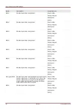
Page 1063: ...ip Command ExP 2 TripCmd Signal Trip Command ExP 3 TripCmd Signal Trip Command ExP 4 TripCmd Signal Trip Command Ext Sudd Press TripCmd Signal Trip Command Ext Oil Temp TripCmd Signal Trip Command Ext...

Page 1064: ...ith the setpoint times The breaker in the higher level section switches off Re connect the control cable to the breaker TCS Trip Circuit Supervision 74TC Available elements TCS The trip circuit monito...

Page 1065: ...e serves also as supply voltage for the digital inputs and so the supply voltage failure of a trip circuit can be detected directly In order to identify a conductor failure in the trip circuit on the...

Page 1066: ...CB position indicator normal open position indicator normal closed TCS trip coil 52a 52b TCS Alarm digital input Device X t t TCS 0 digital input X 1 Either CB Mode Closed This signal is the output of...

Page 1067: ...CDLV4 2E L L LS Trip CB position indicator normal open TCS trip coil TCS Alarm digital input CB Pos ON 52a Device CB Either CB Mode Closed X X t t TCS 0 digital input This signal is the output of the...

Page 1068: ...Supervision Device Planning Parameters of the Trip Circuit Supervision Parameter Description Options Default Menu path Mode Mode do not use use do not use Device planning 1068 MCDLV4 DOK HB MCDLV4 2E...
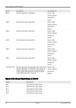
Page 1069: ...trip coil when the breaker is closed 1 n Dig Inputs Protection Para Global Prot Para Supervision TCS Input 2 Select the input configured to monitor the trip coil when the breaker is open Only availabl...

Page 1070: ...Supervision 1070 MCDLV4 DOK HB MCDLV4 2E...

Page 1071: ...allow or inactivate disallow blocking of the module stage This parameter is only effective if a signal is assigned to the corresponding global protection parameter If the signal becomes true those mod...

Page 1072: ...n Para Global Prot Para Supervision TCS ExBlo1 I Module input state External blocking1 Protection Para Global Prot Para Supervision TCS ExBlo2 I Module input state External blocking2 Protection Para G...

Page 1073: ...st of the trip circuit supervision Procedure part 1 Simulate failure of the control voltage in the power circuits Successful test result part 1 After expiry of t TCS the trip circuit supervision TCS o...

Page 1074: ...KI IG 0 KI represents a correction factor which takes the different transformation ratio of the phase and earth current transformers into account The device automatically calculates this factor from t...

Page 1075: ...nt measuring e g normally via a cable type CT the supervision function should be deactivated 1075 MCDLV4 DOK HB MCDLV4 2E Please Refer To Diagram Blockings IG calculated IL1 CTS Alarm CTS Stage is not...

Page 1076: ...ange Default Menu path ExBlo1 External blocking of the module if blocking is activated allowed within a parameter set and if the state of the assigned signal is true 1 n Assignment List Protection Par...

Page 1077: ...order to prevent faulty tripping of phase selective protection functions that use the current as tripping criterion If the difference of the measured earth current and the calculated value I0 is high...

Page 1078: ...Global Prot Para Supervision CTS ExBlo2 I Module input state External blocking2 Protection Para Global Prot Para Supervision CTS Current Transformer Supervision Signals Outputs States Signal Descripti...

Page 1079: ...metrical current system approx nominal current to the secondary side Disconnect the current of one phase from one of the measuring inputs the symmetrical feeding at secondary side has to be maintained...

Page 1080: ...er Field Para VT VT Winding Side The LOP function detects the loss of voltage in any of the voltage input measuring circuits Faulty tripping of protective elements that take voltage into account can b...

Page 1081: ...tive Otherwise the Measuring circuit supervision cannot block elements in case of a loss of potential How to make the Loss of Potential Evaluating Measured Quantities effective The Loss of Potential r...

Page 1082: ...parameter LOP Ex FF VT that represents the state of the automatic circuit breaker of the phase voltage transformer Set the parameter Measuring Crcuit Supervison active within all those protective elem...

Page 1083: ...OP Ex FF EVT 1 n Assignment List 38b LOP Ex FF VT I 38bc LOP Ex FF EVT I LOP Ex FF VT LOP Ex FF VT VL1 VL12 VL2 VL23 VL3 VL31 VL23 VL31 0 5 VL12 180 VL12 VL31 0 5 VL23 180 VL12 VL23 0 5 VL31 180 1 VT...

Page 1084: ...ExBlo1 External blocking of the module if blocking is activated allowed within a parameter set and if the state of the assigned signal is true 1 n Assignment List Protection Para Global Prot Para Supe...

Page 1085: ...tive element will block the Loss of Potential Detection Blo Trigger Protection Para Global Prot Para Supervision LOP Ex FF VT Alarm Fuse Failure Voltage Transformers 1 n Assignment List Protection Par...

Page 1086: ...tween load current and overcurrent A current above this threshold will be seen as overcurrent and LOP will be inhibited If the current detector identifies load current as overcurrent threshold to low...

Page 1087: ...t An Alarm of this protective element will block the Loss of Potential Detection Protection Para Global Prot Para Supervision LOP Blo Trigger3 I State of the module input An Alarm of this protective e...

Page 1088: ...arth Voltage Transformers Blocking Trigger Name Description No assignment I 1 Alarm Signal Alarm I 2 Alarm Signal Alarm I 3 Alarm Signal Alarm I 4 Alarm Signal Alarm I 5 Alarm Signal Alarm I 6 Alarm S...

Page 1089: ...less 0 01 Vn Volt The residual voltage is less than 0 01 Vn Volt or the V2 V1 ratio is greater 40 All three phase currents are less than the load current overcurrent detection I threshold The residual...

Page 1090: ...blocked by the Loss of Potential supervision like undervoltage protection voltage controlled overcurrent protection Check those protective elements if they are blocked if the Loss of Potential superv...

Page 1091: ...e device Procedure Turn off the automatic circuit breaker of the VTs all poles to be dead Successful test result The state of the respective digital input changes All protective elements are blocked w...

Page 1092: ...VT If the check of a CT VT finds that the actual phase sequence is different from the setting under Field Para then the respective signal becomes true active The phase sequence supervision is especia...

Page 1093: ...threshold Monitoring of the communication between Main and Digital Signal Processor DSP The cyclic measured value processing of the DSP is monitored by the main processor The device will be rebooted i...

Page 1094: ...ice memory load internal resources An internal module monitors the system utilization The module for the supervision of the system utilization initiates in case of a fatal error a reboot of the device...

Page 1095: ...5 outdated 6 Unknown Error Source Reboot due to unknown error source 7 Forced Reboot initiated by the main processor The main processor identified invalid conditions or data 8 Exceeded Time Limit of t...

Page 1096: ...t error code e g E01487 In addition to the recorders messages and display information that can be accessed by the user there may exist additional error information accessible by the Service Staff Thes...

Page 1097: ...eration Acknowledge Signals Output States of the Self Supvervision Signal Description System Error Signal Device Failure SelfSuperVision Contact Signal SelfSuperVision Contact Counter Values of the Se...

Page 1098: ...n pickups protective function states breaker states system alarms and module inputs The user can use the outputs signals of a Logic Equation as inputs in higher equations e g the output signal of Logi...

Page 1099: ...ve inactive Inverting1 1 n Assignment List LE x Input2 active inactive Inverting2 1 n Assignment List LE x Input3 active inactive Inverting3 1 n Assignment List LE x Input4 active inactive Inverting4...

Page 1100: ...output of the gate can be delayed The user has the option to set an On and an Off delay Latching The logic equations issues two signals An unlatched and a latched signal The latched output is also ava...

Page 1101: ...uses the output signal of Logic Equation n as input of Logic Equation n 1 If the state of Logic Equation n changes the state of the output of Logic Equation n 1 will be updated within the same cycle...

Page 1102: ...Logic Equation2 LE2 Input2 LE2 Input3 LE2 Input4 Output of Logic Equation 2 Logic Equation1 LE1 Input2 LE1 Input3 LE1 Input4 Output of Logic Equation 1 Logic Equation3 LE3 Input1 LE3 Input2 LE3 Input3...

Page 1103: ...If required configure the timer On delay and Off delay If the latched output signal is used assign a reset signal to the reset input Within the status display the user can check the status of the log...

Page 1104: ...c Device Planning Parameters of the Programmable Logic Parameter Description Options Default Menu path No of Equations Number of required Logic Equations 0 5 10 20 40 80 20 Device planning 1104 MCDLV4...

Page 1105: ...ogics LE 1 LE1 Inverting2 Inverting the input signals Only available if an input signal has been assigned inactive active inactive Logics LE 1 LE1 Input3 Assignment of the Input Signal 1 n Assignment...

Page 1106: ...00s Logics LE 1 LE1 Reset Latched Reset Signal for the Latching 1 n Assignment List Logics LE 1 LE1 Inverting Reset Inverting Reset Signal for the Latching inactive active inactive Logics LE 1 LE1 Inv...

Page 1107: ...Gate In2 I State of the module input Assignment of the Input Signal Logics LE 1 LE1 Gate In3 I State of the module input Assignment of the Input Signal Logics LE 1 LE1 Gate In4 I State of the module...

Page 1108: ...le Logic Outputs Signal Description LE1 Gate Out Signal Output of the logic gate LE1 Timer Out Signal Timer Output LE1 Out Signal Latched Output Q LE1 Out inverted Signal Negated Latched Output Q NOT...

Page 1109: ...ation and safety regulations for working at electrical power installations must always to be followed e g VDE EN DIN IEC Prior to the initial voltage connection the following must be guaranteed Correc...

Page 1110: ...s and relay functions these have to be provided with the relevant alarm and tripping functions of the respective protection functions elements This has to be tested in practical operation Check of all...

Page 1111: ...no voltages that could lead to personal injury Plug out the terminals at the rear side of the device Do not pull any cable pull on the plugs If it is stuck use for example a screw driver Fasten the ca...

Page 1112: ...nu Service General the user can initiate a reboot of the device Phase Sequence Within the menu Operation Status Display Supervision Phase Sequence there are signals showing whether the phase sequence...

Page 1113: ...timeout they will only keep their Force Position as long as this timer runs If the timer expires the relay will operate normally If they are set as Permanent they will keep the Force Position continu...

Page 1114: ...aintenance is complete If they are not armed the protective device WILL NOT provide protection Zone Interlocking Output and the Supervision Contact cannot be disarmed Within this mode Service Test Mod...

Page 1115: ...output contact will be disarmed if it s not latched and There is no running t OFF delay timer hold time of a relay output contact and The DISARM Control is set to active and The Direct Command Disarm...

Page 1116: ...ce Test Mode URTD RTD temperatures can be set by force Permanent or Via timeout If they are set with a timeout they will keep their Forced Temperature only as long as this timer runs If the timer expi...

Page 1117: ...alog Output x Analog Outputs can be set by force Permanent or Via timeout If they are set with a timeout they will only keep their Forced Value as long as this timer runs If the timer expires the Anal...

Page 1118: ...ts can be set by force Permanent or Via timeout If they are set with a timeout they will only keep their Forced Value as long as this timer runs If the timer expires the Analog Input will operate norm...

Page 1119: ...where all protection functions are deactivated This is necessary to re initialize all protection modules and related filters and set them to a healthy new state The states are recorded by the Event an...

Page 1120: ...whether the protective device correctly generates a trip decision so that it is not necessary to always wait until the regular end of the Failure state It is possible to assign the trip signal to Ex...

Page 1121: ...Test Mode Sgen Process 2 TripCmd Mode With TripCmd Manual start stop by external signal Force Post As soon as this signal becomes true the Fault Simulation will be forced to switch into the Post Fail...

Page 1122: ...The simultaneous start of the Fault Simulator takes into account the normal propagation delay of the Protection Communication that means First the trigger signal is sent to the remote device then the...

Page 1123: ...Simulator is started and no trigger signal is sent to the remote device After all the behavior of the local device is exactly like starting the Fault Simulator on a stand alone protective device If th...

Page 1124: ...Service Test Prot inhibit Sgen Configuration Times FaultSimulation Duration of Fault Simulation 0 00 10800 00s 0 0s Service Test Prot inhibit Sgen Configuration Times PostFault PostFault 0 00 300 00s...

Page 1125: ...Service Test Prot inhibit Sgen Process Ex ForcePost Force Post state Abort simulation 1 n Assignment List Service Test Prot inhibit Sgen Process Voltage Parameter of the Failure Simulator Parameter D...

Page 1126: ...n Configuration PreFault VT phi VL2 Start Position respectively Start Angle of the Voltage Phasor during Pre Phase phase L2 360 360 240 Service Test Prot inhibit Sgen Configuration PreFault VT phi VL3...

Page 1127: ...hibit Sgen Configuration FaultSimulation VT VL3 Voltage Fundamental Magnitude in Fault State phase L3 0 00 2 00Vn 0 29Vn Service Test Prot inhibit Sgen Configuration FaultSimulation VT VX Voltage Fund...

Page 1128: ...e L3 360 360 120 Service Test Prot inhibit Sgen Configuration FaultSimulation VT phi VX meas Start Position respectively Start Angle of the Voltage Phasor during Fault Phase VX 360 360 0 Service Test...

Page 1129: ...ion PostFault VT phi VL1 Start Position respectively Start Angle of the Voltage Phasor during Post phase phase L1 360 360 0 Service Test Prot inhibit Sgen Configuration PostFault VT phi VL2 Start Posi...

Page 1130: ...in Pre State phase L1 0 00 40 00In 0 0In Service Test Prot inhibit Sgen Configuration PreFault CT Local IL2 Current Fundamental Magnitude in Pre State phase L2 0 00 40 00In 0 0In Service Test Prot inh...

Page 1131: ...e Test Prot inhibit Sgen Configuration PreFault CT Local phi IL3 Start Position respectively Start Angle of the Current Phasor during Pre Phase phase L3 360 360 120 Service Test Prot inhibit Sgen Conf...

Page 1132: ...FaultSimulation CT Local IG meas Current Fundamental Magnitude in Fault State IG 0 00 25 00In 0 0In Service Test Prot inhibit Sgen Configuration FaultSimulation CT Local phi IL1 Start Position respect...

Page 1133: ...lt Phase IG 360 360 0 Service Test Prot inhibit Sgen Configuration FaultSimulation CT Local IL1 Current Fundamental Magnitude during Post phase phase L1 0 00 40 00In 0 0In Service Test Prot inhibit Sg...

Page 1134: ...iguration PostFault CT Local phi IL2 Start Position respectively Start Angle of the Current Phasor during Post phase phase L2 360 360 240 Service Test Prot inhibit Sgen Configuration PostFault CT Loca...

Page 1135: ...ion Service Test Prot inhibit Sgen Process Signals of the Failure Simulator States of the Outputs Signal Description Manual Start Fault Simulation has been started manually Manual Stop Fault Simulatio...

Page 1136: ...t parameters inactive active inactive Service Test Prot inhibit Sgen Process Failure Simulator Values Value Description Default Size Menu path State Wave generation states 0 Off 1 PreFault 2 Fault 3 P...

Page 1137: ...13123 35 ft altitude apply a changed classification of the operating and test voltages may be necessary Degree of Protection EN 60529 HMI front panel with seal IP54 HMI front panel without seal IP50...

Page 1138: ...8 Pushbottons 19 173 mm 6 811 212 7 mm 8 374 183 mm 7 205 212 7 mm 8 374 173 mm 6 811 4U 212 7 mm 8 374 42 HP Housing depth incl terminals 208 mm 8 189 Material housing Aluminum extruded section Mater...

Page 1139: ...ase current inputs at In 1 A S 25 mVA at In 5 A S 90 mVA Earth current input at In 1 A S 25 mVA at In 5 A S 90 mVA Sensitive earth1 current input at 0 1 A 1A S 7 mVA 550 mVA at 0 5 A 5A S 10 mVA 870 m...

Page 1140: ...ltages 60 520 V can be configured Max measuring range 800 V AC Continuous loading capacity 800 V AC Power consumption at Vn 100 V S 22 mVA at Vn 110 V S 25 mVA at Vn 230 V S 110 mVA at Vn 400 V S 330...

Page 1141: ...o output relays or digital inputs Nominal voltages 60 200 V can be configured Max measuring range 300 V AC Continuous loading capacity 300 V AC Power consumption at Vn 100 V S 22 mVA at Vn 110 V S 25...

Page 1142: ...t 18 A peak value for 0 25 ms 12 A peak value for 1 ms The voltage supply must be protected by a fuse of 2 5 A time lag miniature fuse 5x20 mm approx 1 5 x 0 8 according to IEC 60127 3 5 A time lag mi...

Page 1143: ...kground illumination Resolution graphics display 128 x 128 pixel LED Type Two colored red green Number of LEDs Housing B2 15 Front Interface USB Type Mini B Real Time Clock Running reserve of the real...

Page 1144: ...old 1 ON Switching threshold 1 OFF min 19 2 V DC max 9 6 V DC Un 48 V 60V DC Switching threshold 2 ON Switching threshold 2 OFF Min 42 6 V DC max 21 3 V DC Un 110 V AC DC Switching threshold 3 ON Swit...

Page 1145: ...e Reset time typ 7 ms typ 3 ms Contact type 1 changeover contact or normally open or normally closed Terminals Screw type terminals The operating and reset times are the pure hardware related switchin...

Page 1146: ...inimum Optical Input Power 24 0 dBm Minimum Optical Output Power 19 8 dBm with 50 125 m fiber 16 0 dBm with 62 5 125 m fiber 12 5 dBm with 100 145 m fiber 8 5 dBm with 200 m HCS fiber Maximum Link Len...

Page 1147: ...0 dBm Minimum Optical Output Power 22 5 dBm with 50 125 m fiber 19 0 dBm with 62 5 125 m fiber Maximum Link Length approx 2 km depending on link attenuation availability depends on device URTD Interf...

Page 1148: ...he fiber optic connection and configuration of both devices is correct After approximately 2 minutes depending on the configuration the boot phase is completed HMI and communication initialized The Pr...

Page 1149: ...rm please see chapter Service Every 1 4 years depending on ambient conditions Battery The device checks the battery as part of its Self Supervision therefore no dedicated testing activities are requir...

Page 1150: ...utz KEMA EAC applies to MRU4 applies to MCA4 applies to MRDT4 MCA4 MRA4 MRI4 MRU4 Design Standards Generic standard EN 61000 6 2 2005 EN 61000 6 3 2006 Product standard IEC 60255 1 2009 IEC 60255 27 2...

Page 1151: ...C 60255 27 10 5 3 2 IEC 60255 5 EN 50178 All circuits to other circuits and exposed conductive parts Except interfaces and Voltage measuring input 2 5 kV eff 50Hz 1 min 1 5 kV DC 1 min 3 kV eff 50 Hz...

Page 1152: ...s to earth 2 kV Electrical discharge immunity test ESD IEC 60255 22 2 IEC 61000 4 2 class 3 Air discharge Contact discharge 8 kV 6 kV Radiated radio frequency electromagnetic field immunity test IEC 6...

Page 1153: ...o interference suppression test IEC CISPR22 IEC60255 26 DIN EN 55022 150kHz 30MHz Limit value class B Radio interference radiation test IEC CISPR22 IEC60255 25 DIN EN 55022 30MHz 1GHz Limit value clas...

Page 1154: ...2K2 2B1 2C1 2S1 2M2 but min 30 C IEC 60721 3 3 Classification of ambient conditions Stationary use at weather protected locations 3K6 3B1 3C1 3S1 3M2 but min 20 C max 60 C Test Ad Cold IEC 60068 2 1 T...

Page 1155: ...Temperature Change IEC 60255 6 12 3 5 IEC 60068 2 14 Temperature cycle test duration 60 C 20 C 5 1 C 5min Test BD Dry Heat Transport and storage test IEC 60255 6 12 3 3 IEC 60068 2 2 Temperature test...

Page 1156: ...IEC 60068 2 27 IEC 60255 21 2 class 1 Shock response test 5 gn 11 ms 3 impulses in each direction Shock resistance test 15 gn 11 ms 3 impulses in each direction Test Eb Shockendurance test IEC 60068...

Page 1157: ...Signal Phase current failure forward direction Prot I dir rev Signal Phase current failure reverse direction Prot I dir n poss Signal Phase fault missing reference voltage Prot IG calc dir fwd Signal...

Page 1158: ...or more IL_On inputs are active SG 1 Interl OFF Signal One or more IL_Off inputs are active SG 1 CES succesf Signal Command Execution Supervision Switching command executed successfully SG 1 CES Distu...

Page 1159: ...ate of the module input Acknowledgement Signal only for automatic acknowledgement Module input signal SG 1 Interl ON1 I State of the module input Interlocking of the ON command SG 1 Interl ON2 I State...

Page 1160: ...r more IL_Off inputs are active SG 2 CES succesf Signal Command Execution Supervision Switching command executed successfully SG 2 CES Disturbed Signal Command Execution Supervision Switching Command...

Page 1161: ...gement Module input signal SG 2 Interl ON1 I State of the module input Interlocking of the ON command SG 2 Interl ON2 I State of the module input Interlocking of the ON command SG 2 Interl ON3 I State...

Page 1162: ...ervision Switching command executed successfully SG 3 CES Disturbed Signal Command Execution Supervision Switching Command unsuccessful Switchgear in disturbed position SG 3 CES Fail TripCmd Signal Co...

Page 1163: ...g of the ON command SG 3 Interl ON2 I State of the module input Interlocking of the ON command SG 3 Interl ON3 I State of the module input Interlocking of the ON command SG 3 Interl OFF1 I State of th...

Page 1164: ...sturbed Signal Command Execution Supervision Switching Command unsuccessful Switchgear in disturbed position SG 4 CES Fail TripCmd Signal Command Execution Supervision Command execution failed because...

Page 1165: ...rlocking of the ON command SG 4 Interl OFF1 I State of the module input Interlocking of the OFF command SG 4 Interl OFF2 I State of the module input Interlocking of the OFF command SG 4 Interl OFF3 I...

Page 1166: ...led because trip command is pending SG 5 CES SwitchDir Signal Command Execution Supervision respectively Switching Direction Control This signal becomes true if a switch command is issued even though...

Page 1167: ...module input Interlocking of the OFF command SG 5 Interl OFF3 I State of the module input Interlocking of the OFF command SG 5 SCmd ON I State of the module input Switching ON Command e g the state o...

Page 1168: ...trol This signal becomes true if a switch command is issued even though the switchgear is already in the requested position Example A switchgear that is already OFF should be switched OFF again doubly...

Page 1169: ...ocking of the OFF command SG 6 SCmd ON I State of the module input Switching ON Command e g the state of the Logics or the state of the digital input SG 6 SCmd OFF I State of the module input Switchin...

Page 1170: ...gnal Restraining of the differential protection by means of rising the tripping curve Id Slope Blo L1 Slope Blo L1 Id Slope Blo L2 Slope Blo L2 Id Slope Blo L3 Slope Blo L3 Id Restraining L1 Restraini...

Page 1171: ...and IdH ExBlo1 I Module input state External blocking1 IdH ExBlo2 I Module input state External blocking2 IdH ExBlo TripCmd I Module input state External Blocking of the Trip Command IdG active Signal...

Page 1172: ...gnal Blocking the trip command by an inrush I 1 Alarm L1 Signal Alarm L1 I 1 Alarm L2 Signal Alarm L2 I 1 Alarm L3 Signal Alarm L3 I 1 Alarm Signal Alarm I 1 Trip L1 Signal General Trip Phase L1 I 1 T...

Page 1173: ...I Module input state External blocking1 I 2 ExBlo2 I Module input state External blocking2 I 2 ExBlo TripCmd I Module input state External Blocking of the Trip Command I 2 Ex rev Interl I Module input...

Page 1174: ...terl Signal External reverse Interlocking I 4 Blo TripCmd Signal Trip Command blocked I 4 ExBlo TripCmd Signal External Blocking of the Trip Command I 4 IH2 Blo Signal Blocking the trip command by an...

Page 1175: ...Signal Adaptive Parameter 1 I 5 AdaptSet 2 Signal Adaptive Parameter 2 I 5 AdaptSet 3 Signal Adaptive Parameter 3 I 5 AdaptSet 4 Signal Adaptive Parameter 4 I 5 ExBlo1 I Module input state External bl...

Page 1176: ...tSet4 I Module input state Adaptive Parameter4 IG 1 active Signal active IG 1 ExBlo Signal External Blocking IG 1 Ex rev Interl Signal External reverse Interlocking IG 1 Blo TripCmd Signal Trip Comman...

Page 1177: ...I Module input state External reverse interlocking IG 2 AdaptSet1 I Module input state Adaptive Parameter1 IG 2 AdaptSet2 I Module input state Adaptive Parameter2 IG 2 AdaptSet3 I Module input state...

Page 1178: ...aptive Parameter 4 IG 4 ExBlo1 I Module input state External blocking1 IG 4 ExBlo2 I Module input state External blocking2 IG 4 ExBlo TripCmd I Module input state External Blocking of the Trip Command...

Page 1179: ...te External Blocking of the Trip Command V 1 active Signal active V 1 ExBlo Signal External Blocking V 1 Blo TripCmd Signal Trip Command blocked V 1 ExBlo TripCmd Signal External Blocking of the Trip...

Page 1180: ...External Blocking of the Trip Command V 3 Alarm L1 Signal Alarm L1 V 3 Alarm L2 Signal Alarm L2 V 3 Alarm L3 Signal Alarm L3 V 3 Alarm Signal Alarm voltage stage V 3 Trip L1 Signal General Trip Phase...

Page 1181: ...m Signal Alarm voltage stage V 5 Trip L1 Signal General Trip Phase L1 V 5 Trip L2 Signal General Trip Phase L2 V 5 Trip L3 Signal General Trip Phase L3 V 5 Trip Signal Trip V 5 TripCmd Signal Trip Com...

Page 1182: ...e External Blocking of the Trip Command delta phi active Signal active delta phi ExBlo Signal External Blocking delta phi Blo by V Signal Module is blocked by undervoltage delta phi Blo TripCmd Signal...

Page 1183: ...Signal External Blocking of the Trip Command Q Alarm Signal Alarm Power Protection Q Trip Signal Trip Power Protection Q TripCmd Signal Trip Command Q ExBlo1 I Module input state External blocking Q E...

Page 1184: ...ExBlo TripCmd I Module input state External Blocking of the Trip Command VG 1 active Signal active VG 1 ExBlo Signal External Blocking VG 1 Blo TripCmd Signal Trip Command blocked VG 1 ExBlo TripCmd S...

Page 1185: ...e External blocking2 V012 2 ExBlo TripCmd I Module input state External Blocking of the Trip Command V012 3 active Signal active V012 3 ExBlo Signal External Blocking V012 3 Blo TripCmd Signal Trip Co...

Page 1186: ...ExBlo TripCmd I Module input state External Blocking of the Trip Command f 1 active Signal active f 1 ExBlo Signal External Blocking f 1 Blo by V Signal Module is blocked by undervoltage f 1 Blo Trip...

Page 1187: ...al Blocking of the Trip Command f 3 Alarm f Signal Alarm Frequency Protection f 3 Alarm df dt DF DT Alarm instantaneous or average value of the rate of frequency change f 3 Alarm delta phi Signal Alar...

Page 1188: ...he limit f 5 Trip df dt DF DT Signal Trip df dt or DF DT f 5 Trip delta phi Signal Trip Vector Surge f 5 Trip Signal Trip Frequency Protection collective signal f 5 TripCmd Signal Trip Command f 5 ExB...

Page 1189: ...er Protection PQS 2 TripCmd Signal Trip Command PQS 2 ExBlo1 I Module input state External blocking PQS 2 ExBlo2 I Module input state External blocking PQS 2 ExBlo TripCmd I Module input state Externa...

Page 1190: ...nal Trip Power Protection PQS 6 TripCmd Signal Trip Command PQS 6 ExBlo1 I Module input state External blocking PQS 6 ExBlo2 I Module input state External blocking PQS 6 ExBlo TripCmd I Module input s...

Page 1191: ...al External Blocking ReCon 1 Blo by Meas Ciruit Superv Signal Module blocked by measuring cirucuit supervision ReCon 1 Release Energy Resource Signal Release Energy Resource ReCon 1 ExBlo1 I Module in...

Page 1192: ...1 Release Signal I Minimum Current in order to prevent faulty tripping Module will be released if the current exceeds this value UFLS VLL min Signal Minimum Voltage UFLS Power Angle Signal Trigger Phi...

Page 1193: ...or this time after the reset signal e g digital input or Scada has been detected AR Blo Signal Auto Reclosure is blocked AR t Blo Reset Signal Delay Timer for resetting the AR blocking The release de...

Page 1194: ...the state of the assigned signal is true If the state of this function is true the AR will be aborted Sync active Signal active Sync ExBlo Signal External Blocking Sync LiveBus Signal Live Bus flag 1...

Page 1195: ...ocking2 V f 2 ExBlo TripCmd I Module input state External Blocking of the Trip Command SOTF active Signal active SOTF ExBlo Signal External Blocking SOTF Ex rev Interl Signal External reverse Interloc...

Page 1196: ...Signal External Blocking of the Trip Command ExP 2 Alarm Signal Alarm ExP 2 Trip Signal Trip ExP 2 TripCmd Signal Trip Command ExP 2 ExBlo1 I Module input state External blocking1 ExP 2 ExBlo2 I Modu...

Page 1197: ...l Trip Command Ext Sudd Press ExBlo1 I Module input state External blocking1 Ext Sudd Press ExBlo2 I Module input state External blocking2 Ext Sudd Press ExBlo TripCmd I Module input state External Bl...

Page 1198: ...Alarm I Module input state Alarm Ext Temp Superv 1 Trip I Module input state Trip Ext Temp Superv 2 active Signal active Ext Temp Superv 2 ExBlo Signal External Blocking Ext Temp Superv 2 Blo TripCmd...

Page 1199: ...ive Status of received Signal from remote device Permissive signal is considered Trip Trans Rx Trip3 Rx Receive Status of received Signal from remote device Permissive signal is considered Trip Trans...

Page 1200: ...s of received Signal from remote device Sig Trans Rx Signal4 Rx Receive Status of received Signal from remote device Sig Trans Rx Signal5 Rx Receive Status of received Signal from remote device Sig Tr...

Page 1201: ...al active CBF ExBlo Signal External Blocking CBF Waiting for Trigger Waiting for Trigger CBF running Signal CBF Module started CBF Alarm Signal Circuit Breaker Failure CBF Lockout Signal Lockout CBF R...

Page 1202: ...r5 I State of the module input An Alarm of this protective element will block the Loss of Potential Detection PQSCr Cr Oflw Ws Net Signal Counter Overflow Ws Net PQSCr Cr Oflw Wp Net Signal Counter Ov...

Page 1203: ...Trip Watt Demand Signal Trip averaged Active Power exceeded SysA Trip VAr Demand Signal Trip averaged Reactive Power exceeded SysA Trip VA Demand Signal Trip averaged Apparent Power exceeded SysA Tri...

Page 1204: ...utput Relay BO Slot X4 BO 4 Signal Binary Output Relay BO Slot X4 BO 5 Signal Binary Output Relay BO Slot X4 DISARMED Signal CAUTION RELAYS DISARMED in order to safely perform maintenance while elimin...

Page 1205: ...Output has been set by force That means that the state of at least one Relay is forced and hence does not show the state of the assigned signals Event rec Res all records Signal All records deleted D...

Page 1206: ...t of the protective device DNP3 BinaryOutput7 Virtual Digital Output DNP This corresponds to a virtual binary input of the protective device DNP3 BinaryOutput8 Virtual Digital Output DNP This correspo...

Page 1207: ...rtual binary input of the protective device DNP3 BinaryOutput30 Virtual Digital Output DNP This corresponds to a virtual binary input of the protective device DNP3 BinaryOutput31 Virtual Digital Outpu...

Page 1208: ...ual binary output of the protective device DNP3 BinaryInput21 I Virtual Digital Input DNP This corresponds to a virtual binary output of the protective device DNP3 BinaryInput22 I Virtual Digital Inpu...

Page 1209: ...ual binary output of the protective device DNP3 BinaryInput44 I Virtual Digital Input DNP This corresponds to a virtual binary output of the protective device DNP3 BinaryInput45 I Virtual Digital Inpu...

Page 1210: ...the protective device Modbus Transmission RTU Signal SCADA active Modbus Transmission TCP Signal SCADA active Modbus Scada Cmd 1 Scada Command Modbus Scada Cmd 2 Scada Command Modbus Scada Cmd 3 Scad...

Page 1211: ...the module input Config Bin Inp Modbus Config Bin Inp19 I State of the module input Config Bin Inp Modbus Config Bin Inp20 I State of the module input Config Bin Inp Modbus Config Bin Inp21 I State o...

Page 1212: ...IO Ind IEC61850 VirtInp14 Signal Virtual Input IEC61850 GGIO Ind IEC61850 VirtInp15 Signal Virtual Input IEC61850 GGIO Ind IEC61850 VirtInp16 Signal Virtual Input IEC61850 GGIO Ind IEC61850 VirtInp17...

Page 1213: ...IEC61850 Quality of GGIO In12 Self Supervision of the GGIO Input IEC61850 Quality of GGIO In13 Self Supervision of the GGIO Input IEC61850 Quality of GGIO In14 Self Supervision of the GGIO Input IEC61...

Page 1214: ...bit that can be set by clients like e g SCADA Single Point Controllable Status Output IEC61850 SPCSO6 Status bit that can be set by clients like e g SCADA Single Point Controllable Status Output IEC61...

Page 1215: ...e g SCADA Single Point Controllable Status Output IEC61850 SPCSO28 Status bit that can be set by clients like e g SCADA Single Point Controllable Status Output IEC61850 SPCSO29 Status bit that can be...

Page 1216: ...te Binary state of the Virtual Output GGIO IEC61850 VirtOut27 I Module input state Binary state of the Virtual Output GGIO IEC61850 VirtOut28 I Module input state Binary state of the Virtual Output GG...

Page 1217: ...mporarily forced to be deactivated blocked ProtCom Qual Warn Error Rate is above warning level ProtCom Comm Ok Protection communication Ok Measuring systems is synchron with remote device ProtCom Fram...

Page 1218: ...device e g logic funtions IRIG B Control Signal11 Signal IRIG B Control Signal The external IRIG B generator can set these signals They can be used for further control procedures inside the device e...

Page 1219: ...ogics LE1 Gate In4 I State of the module input Assignment of the Input Signal Logics LE1 Reset Latch I State of the module input Reset Signal for the Latching Logics LE2 Gate Out Signal Output of the...

Page 1220: ...E6 Timer Out Signal Timer Output Logics LE6 Out Signal Latched Output Q Logics LE6 Out inverted Signal Negated Latched Output Q NOT Logics LE6 Gate In1 I State of the module input Assignment of the In...

Page 1221: ...e Input Signal Logics LE10 Gate In2 I State of the module input Assignment of the Input Signal Logics LE10 Gate In3 I State of the module input Assignment of the Input Signal Logics LE10 Gate In4 I St...

Page 1222: ...3 I State of the module input Assignment of the Input Signal Logics LE14 Gate In4 I State of the module input Assignment of the Input Signal Logics LE14 Reset Latch I State of the module input Reset S...

Page 1223: ...of the Input Signal Logics LE18 Gate In4 I State of the module input Assignment of the Input Signal Logics LE18 Reset Latch I State of the module input Reset Signal for the Latching Logics LE19 Gate...

Page 1224: ...of the Input Signal Logics LE22 Gate In4 I State of the module input Assignment of the Input Signal Logics LE22 Reset Latch I State of the module input Reset Signal for the Latching Logics LE23 Gate...

Page 1225: ...of the Input Signal Logics LE26 Gate In4 I State of the module input Assignment of the Input Signal Logics LE26 Reset Latch I State of the module input Reset Signal for the Latching Logics LE27 Gate...

Page 1226: ...of the Input Signal Logics LE30 Gate In4 I State of the module input Assignment of the Input Signal Logics LE30 Reset Latch I State of the module input Reset Signal for the Latching Logics LE31 Gate...

Page 1227: ...of the Input Signal Logics LE34 Gate In4 I State of the module input Assignment of the Input Signal Logics LE34 Reset Latch I State of the module input Reset Signal for the Latching Logics LE35 Gate...

Page 1228: ...of the Input Signal Logics LE38 Gate In4 I State of the module input Assignment of the Input Signal Logics LE38 Reset Latch I State of the module input Reset Signal for the Latching Logics LE39 Gate...

Page 1229: ...of the Input Signal Logics LE42 Gate In4 I State of the module input Assignment of the Input Signal Logics LE42 Reset Latch I State of the module input Reset Signal for the Latching Logics LE43 Gate...

Page 1230: ...of the Input Signal Logics LE46 Gate In4 I State of the module input Assignment of the Input Signal Logics LE46 Reset Latch I State of the module input Reset Signal for the Latching Logics LE47 Gate...

Page 1231: ...of the Input Signal Logics LE50 Gate In4 I State of the module input Assignment of the Input Signal Logics LE50 Reset Latch I State of the module input Reset Signal for the Latching Logics LE51 Gate...

Page 1232: ...of the Input Signal Logics LE54 Gate In4 I State of the module input Assignment of the Input Signal Logics LE54 Reset Latch I State of the module input Reset Signal for the Latching Logics LE55 Gate...

Page 1233: ...of the Input Signal Logics LE58 Gate In4 I State of the module input Assignment of the Input Signal Logics LE58 Reset Latch I State of the module input Reset Signal for the Latching Logics LE59 Gate...

Page 1234: ...of the Input Signal Logics LE62 Gate In4 I State of the module input Assignment of the Input Signal Logics LE62 Reset Latch I State of the module input Reset Signal for the Latching Logics LE63 Gate...

Page 1235: ...of the Input Signal Logics LE66 Gate In4 I State of the module input Assignment of the Input Signal Logics LE66 Reset Latch I State of the module input Reset Signal for the Latching Logics LE67 Gate...

Page 1236: ...of the Input Signal Logics LE70 Gate In4 I State of the module input Assignment of the Input Signal Logics LE70 Reset Latch I State of the module input Reset Signal for the Latching Logics LE71 Gate...

Page 1237: ...of the Input Signal Logics LE74 Gate In4 I State of the module input Assignment of the Input Signal Logics LE74 Reset Latch I State of the module input Reset Signal for the Latching Logics LE75 Gate...

Page 1238: ...of the Input Signal Logics LE78 Gate In4 I State of the module input Assignment of the Input Signal Logics LE78 Reset Latch I State of the module input Reset Signal for the Latching Logics LE79 Gate...

Page 1239: ...set that should become active e g 4 Switch onto parameter set 4 Sys PSS via Inp fct Signal Parameter Set Switch via input function Sys min 1 param changed Signal At least one parameter has been change...

Page 1240: ...I State of the module input respectively of the signal that should activate this Parameter Setting Group Sys PS3 I State of the module input respectively of the signal that should activate this Param...

Page 1241: ...1 DI 7 Signal Digital Input DI Slot X1 DI 8 Signal Digital Input DI Slot X5 DI 1 Signal Digital Input DI Slot X5 DI 2 Signal Digital Input DI Slot X5 DI 3 Signal Digital Input DI Slot X5 DI 4 Signal D...

Page 1242: ...Rx Signal11 Rx Receive Status of received Signal from remote device Sig Trans Rx Signal12 Rx Receive Status of received Signal from remote device Sig Trans Rx Signal13 Rx Receive Status of received S...

Page 1243: ...ut DNP This corresponds to a virtual binary input of the protective device DNP3 BinaryOutput9 Virtual Digital Output DNP This corresponds to a virtual binary input of the protective device DNP3 Binary...

Page 1244: ...l Output DNP This corresponds to a virtual binary input of the protective device DNP3 BinaryOutput30 Virtual Digital Output DNP This corresponds to a virtual binary input of the protective device DNP3...

Page 1245: ...E10 Out Signal Latched Output Q Logics LE10 Out inverted Signal Negated Latched Output Q NOT Logics LE11 Gate Out Signal Output of the logic gate Logics LE11 Timer Out Signal Timer Output Logics LE11...

Page 1246: ...Logics LE20 Out Signal Latched Output Q Logics LE20 Out inverted Signal Negated Latched Output Q NOT Logics LE21 Gate Out Signal Output of the logic gate Logics LE21 Timer Out Signal Timer Output Logi...

Page 1247: ...Logics LE30 Out Signal Latched Output Q Logics LE30 Out inverted Signal Negated Latched Output Q NOT Logics LE31 Gate Out Signal Output of the logic gate Logics LE31 Timer Out Signal Timer Output Logi...

Page 1248: ...Logics LE40 Out Signal Latched Output Q Logics LE40 Out inverted Signal Negated Latched Output Q NOT Logics LE41 Gate Out Signal Output of the logic gate Logics LE41 Timer Out Signal Timer Output Logi...

Page 1249: ...Logics LE50 Out Signal Latched Output Q Logics LE50 Out inverted Signal Negated Latched Output Q NOT Logics LE51 Gate Out Signal Output of the logic gate Logics LE51 Timer Out Signal Timer Output Logi...

Page 1250: ...Logics LE60 Out Signal Latched Output Q Logics LE60 Out inverted Signal Negated Latched Output Q NOT Logics LE61 Gate Out Signal Output of the logic gate Logics LE61 Timer Out Signal Timer Output Logi...

Page 1251: ...Logics LE70 Out Signal Latched Output Q Logics LE70 Out inverted Signal Negated Latched Output Q NOT Logics LE71 Gate Out Signal Output of the logic gate Logics LE71 Timer Out Signal Timer Output Logi...

Page 1252: ...OT Logics LE78 Gate Out Signal Output of the logic gate Logics LE78 Timer Out Signal Timer Output Logics LE78 Out Signal Latched Output Q Logics LE78 Out inverted Signal Negated Latched Output Q NOT L...

Page 1253: ...see operation status of SNTP IEC60870 5 103 Dependent on the time drift of the time generator 1 ms Modbus TCP Dependent on the time drift of the time generator Dependent on the network load Modbus RTU...

Page 1254: ...itive the precision does not depend on the nominal value but is referenced to 100 mA with In 1 A respectively 500 mA with In 5 A Phase to ground and Residual Voltage Measurement Frequency Range 50 Hz...

Page 1255: ...unter error 1 5 of measured energy or 1 5 Sn 1h Power Measurement S P Q 1 of the measured value or 0 1 Sn for fundamental 2 of the measured value or 0 2 Sn for RMS P1 Q1 2 of the measured value or 0 2...

Page 1256: ...ements I x with selected Measuring method I2 Negative phase sequence current Accuracy I 2 of the setting value or 1 In Dropout Ratio 97 or 0 5 In t DEFT 1 or 10 ms Operating Time At testing current 2...

Page 1257: ...Neg I2 V2 10 mA 50 mA 0 35 V 5 mA 25 mA 0 25 V Phase Differential Protection Id Accuracy Id 3 of the setting value or 2 In Operating time Id 2 x pickup step from zero to 200 pickup of 87 Char 40 ms Ty...

Page 1258: ...1 Negative sequence current I2 must be 0 01 x In I1 must be 0 1 x In Voltage Protection V x Accuracy Pickup 1 5 of the setting value or 1 Vn Dropout Ratio Adjustable at least 0 5 Vn t DEFT 1 or 10 ms...

Page 1259: ...higher than 1 1 x Pickup 60 ms at fn or 4 cycles Disengaging Time 85 ms at fn or 5 cycles 1 The V Hz function provides reliable measurements of V Hz for a frequency range of fn 10 if voltage rms is gr...

Page 1260: ...ypically 100 ms typically 70 ms Disengaging time 120 ms 1 Accurracy is given for rated frequency fn 10 2 10 additional tolerance per Hz deviation from nominal frequency fn e g at 45Hz tolerance is 0 1...

Page 1261: ...sengaging time 100 ms Directional Power Protection PQS x with Mode Q Q or Qr Qr Accuracy 1 Threshold 3 or 0 1 Sn Dropout Ratio 97 or 1 VA for Q and Qr 103 or 1 VA for Q and Qr for setting values 0 1 S...

Page 1262: ...102 or 0 5 Vn for VLL f 20 mHz at fn Dropout 0 05 fn t Release 1 or 10 ms Operating Time 100 ms UFLS Tolerance I min 1 5 of the setting value or 1 In Dropout Ratio 95 or 0 5 In V min 1 5 of the setti...

Page 1263: ...Failure Protection CBF Accuracy I CBF 1 5 of the setting value or1 In t CBF 1 or 10 ms Operating Time Starting from I Higher than 1 3 x I CBF 40 ms Disengaging Time 40 ms Trip Circuit Supervision TCS...

Page 1264: ...her For special questions and more detailed information please contact Woodward Kempen GmbH Support Up to date documentation Please check the web site of Woodward Kempen GmbH for the latest revision o...

Page 1265: ...sion in Monitor Direction and the test mode Modbus The transmission of fault values via Modbus protocol has been added For the last fault event all fault values are accessible with addresses above 500...

Page 1266: ...n particular error messages are now accessible under the menu Operation Self Supervision Messages All messages that can potentially appear here are described in a separate document the HighPROTEC Trou...

Page 1267: ...ch 14 Revision NEW made available only to selected customers as a pilot project Date 2017 April 14 Revision NEW Hardware Initial release of a HighPROTEC Line Differential Protection device Software In...

Page 1268: ...lay BO3 3rd binary output relay calc Calculated CB Circuit breaker CBF Module Circuit Breaker Failure protection CD Compact disk Char Curve shape CLPU Cold Load Pickup Module Cmd Command CMN Common in...

Page 1269: ...on of the earth in vertical direction 9 81 m s2 GND Ground h Hour HMI Human machine interface Front of the protective relay HTL Manufacturer internal product designation Hz Hertz I Phase Overcurrent S...

Page 1270: ...rent IRIG Input for time synchronization Clock IRIG B IRIG B Module IT Thermal Characteristic IX 4th measuring input of the current measuring assembly group either ground or neutral current J Joule kg...

Page 1271: ...d circuit board PE Protected Earth p u per unit PF Power Factor Module Ph Phase PQS Power Protection Module pri Primary PROT or Prot Protection Module Master Module PS1 Parameter set 1 PS2 Parameter s...

Page 1272: ...s Laboratories UMZ DEFT definite time tripping characteristic USB Universal serial bus V Voltage stage V Volts V f Overexcitation V012 Symmetrical Components Supervision of the Positive Phase Sequence...

Page 1273: ...age Protection 48 Incomplete Sequence Start up time Supervison 49 Thermal Protection 49M Thermal Motor Protection 49R Thermal Rotor Protection 49S Thermal Stator Protection 50BF Breaker Failure 50 Ove...

Page 1274: ...ock Out 87B Busbar Differential Protection 87G Generator Differential Protection 87GP Generator Phase Differential Protection 87GN Generator Ground Differential Protection 87L Cable and Line Different...

Page 1275: ...However Woodward Kempen GmbH assumes no responsibility unless otherwise expressly undertaken This is the original manual source Woodward Kempen GmbH all rights reserved Woodward Kempen GmbH Krefelder...

Reviews: