W632GU6NB
Publication Release Date: Aug. 20, 2018
Revision: A01
- 18 -
8.3.1
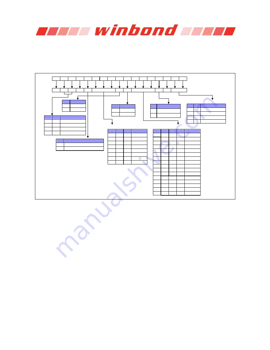
Mode Register MR0
The mode register MR0 stores the data for controlling various operating modes of DDR3L SDRAM. It
controls burst length, read burst type, CAS latency, test mode, DLL reset, WR and DLL control for
precharge Power Down, which include various vendor specific options to make DDR3L SDRAM useful
for various applications. The mode register is written by asserting low on CS#, RAS#, CAS#, WE#,
BA0, BA1 and BA2, while controlling the states of address pins according to the Figure 5 below.
DLL Control for Precharge PD
DLL Reset
A8
MRS mode
WR(cycles)
A3
Read Burst Type
BA1
BA0
A12
A11
A10
A9
A8
A7
A6
A5
A4
A3
A2
A1
A0
0
*1
PPD
WR
DLL
RBT
CL
BL
TM
0
1
No
Yes
BA1
BA0
0
0
0
1
1
0
1
1
MR0
MR1
MR2
MR3
A12
1
0
Slow exit (DLL off)
Fast exit (DLL on)
Burst Length
Address Field
Mode Register 0
Write recovery for Auto precharge
CAS Latency
A5
0
0
1
1
0
0
1
1
A4
0
1
0
1
0
1
1
0
A2
0
0
0
0
0
0
0
0
Latency
Reserved
7
8
9
11
10
5
6
BL
A0
A1
0
0
0
1
8 (Fixed)
BC4 or 8 (on the fly)
A11
0
0
0
0
1
1
1
1
A10
0
0
1
1
0
0
1
1
A9
0
1
0
1
0
1
1
0
16
*2
5
*2
6
*2
7
*2
8
*2
10
*2
14
*2
12
*2
Mode
A7
0
1
Normal
Test
0
1
Nibble Sequential
Interleave
0
0
A13
CL
0
0
0
0
1
1
1
1
1
1
0
1
BC4 (Fixed)
Reserved
BA2
0
*1
0
1
0
0
0
1
1
1
1
Reserved
14
13
0
0
0
0
1
0
1
1
1
Reserved
Reserved
1
0
0
1
1
1
1
0
1
1
1
Reserved
Reserved
Reserved
1
1
1
A6
Notes:
1. BA2 and A13 are
reserved for future use and must be programmed to
“0” during MRS.
2. WR (write recovery for Auto precharge)min in clock cycles is calculated by dividing t
WR
(in nS) by t
CK
(in nS) and rounding
up to the next integer: WRmin[cycles] = Roundup(t
WR
[nS] / t
CK(avg)
[nS]). The WR value in the mode register must be
programmed to be equal or larger than WRmin. The programmed WR value is used with t
RP
to determine t
DAL
.
3. The table only shows the encodings for a given Cas Latency. For actual supported CAS Latency, please refer to
tables for each frequency.
4. The table only shows the encodings for Write Recovery. For actual Write recovery timing, please refer to AC timing table.
Figure 5
– MR0 Definition


