background image


UG:309 

Page 4

Software Installation and Operation

Users downloading the 

Buck GUI

 should save the compressed file in a desired directory. The user should 

unzip the compressed file and run the executable installation file “PicorBuckGuiFull_setup.exe”. The 

installer will then install the Buck GUI in either the default Programs directory or to a directory specified 

by the user. Once the software is installed, the user should next plug in the LinkM™ into a dedicated 

USB port. The LinkM will detect and use a valid driver without the need of installing one. If the LinkM 

device is not detected, the user should consult the Link

homepage

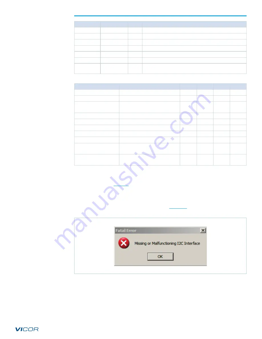
. If the LinkM is not installed, the 

Buck GUI will not start and an error message will be generated like the one shown in Figure 3.

Successful installation of the LinkM Interface should result in a successful start up screen of the Buck 

GUI as shown in Figure 4. First a dialog box will pop up indicating proper detection of the LinkM. When 

the user clicks the “OK” button, that box will disappear. The Buck GUI program screen will appear as 

shown in the bottom half of Figure 4.

Table 2


User‑accessible registers

Table 3


I

2

C™ port specifications

Figure 3


Error message due to missing 

LinkM upon software start

Name

Address HEX

# Bits

Description

TSTMDE[2:0]

18

3

Test mode register used for burning bits into non‑volatile memory

MRGN[3:0]

19

4

Volatile register for output voltage margining

FLT[7:0]

1A

8

Fault Register read only

FREG_CLR

1B

0

Register for clearing the Fault Register‑writing address clears register

ENA_POL

20

1

EN pin polarity programming bit

SYN[3:0]

21

4

SYNC programming. SYN[3] = SYNC polarity

KBIT2

22

1

User kill bit for SYN[3:0] and ENA_POL – 

can not be reversed; 

register is write only, can not be read

Parameter

Conditions

Min

Typ

Max

Units

SCL, SDA V

IH

Rising, 3.3V & 5V bus compatible

2.1

V

SCL, SDA V

IL

Falling 3.3V & 5V bus compatible

1.5

V

SCL, SDA input current 
(sink to hold open pins low)

At 5V

1.8

5

10

µA

SDA V

OL

3mA

0.4

V

ADDR0,1V

MID

V

CC

 = PI33xx‑xx fixed, internal 5.1V

0.4V

CC

0.6V

CC

V

ADDR0,1V

IH

V

CC

 = PI33xx‑xx fixed, internal 5.1V

0.8V

CC

V

ADDR0,1V

IL

V

CC

 = PI33xx‑xx fixed, internal 5.1V

0.1V

CC

0.2V

CC

V

ADDR0,1 hysteresis

0

mV

ADDR0,1 Output resistance 
from ½ V

CC

0.3V

CC

 < ADDRx < 0.7V

CC


V

CC

 = PI33xx‑xx fixed, internal 5.1V

6k

ADDR0,1 Output resistance 
from ½ V

CC

ADDRx < 0.2V

CC

, ADDRx > 0.8V

CC


V

CC

 = PI33xx‑xx fixed, internal 5.1V

70k

Summary of Contents for PI33 EVAL1 Series

Page 1: ...ompatibility The PI33xx xx is hardware compatible with the NXP I2C bus specification Version 2 1 Standard Mode 100kHz January 2000 for all bus timing and voltage resistors levels up to 5 5V maximum The PI33xx xx is configured as an I2C child device with no internal bus pull up or pull down Interface Software Tool The Buck GUI software tool offered by Vicor allows quick access to the one time progr...

Page 2: ...ort The use of USB expansion ports especially those that are heavily loaded is not recommended The LinkM interface can be mounted directly to the PI33xx xx evaluation board using a straight 4 pin header see Figure 1 Users who wish to connect the LinkM in this manner will need to use a male to female USB extension cable This method works very well and is the preferred method Other users may wish to...

Page 3: ...ing of ADR1 and ADR0 A zero or one indicates the logic strength of the bit and NC indicates that the pin is floating or not connected The HEX column indicates the final address in hexadecimal while the DEC column is the decimal address value Table 1 Addressing options See Table 3 where VCC PI33xx xx fixed internal 5 1V bias rail PGND SGND SYNCO PGD Q1 Q2 ADR0 SDA VCC ADR1 EN SYNCI TRK EAO ADJ VS1 ...

Page 4: ...ttom half of Figure 4 Table 2 User accessible registers Table 3 I2C port specifications Figure 3 Error message due to missing LinkM upon software start Name Address HEX Bits Description TSTMDE 2 0 18 3 Test mode register used for burning bits into non volatile memory MRGN 3 0 19 4 Volatile register for output voltage margining FLT 7 0 1A 8 Fault Register read only FREG_CLR 1B 0 Register for cleari...

Page 5: ...be powered on using the proper input voltage value and enabled by the user Failure to apply input voltage will result in the error message shown in Figure 28 see Buck GUI error messages section upon pressing any of the soft buttons on the screen The LinkM should not be removed or installed with the power already applied to the PI33xx xx Always power down the PI33xx xx prior to installing or removi...

Page 6: ...in in a low power state Since it has not entered operate mode the UVLO fault will not be logged If the input voltage is higher than the undervoltage lockout threshold but drops to zero the fault will remain latched as long as there is VCC to the controller Once the controller VCC dips below the minimum value the fault data will not remain valid The fault register will be cleared upon power on rese...

Page 7: ...nges made to this register are dynamic and will change as soon as the command is sent The user simply enters the value they wish to margin and then clicks margin Any value sent to this register will be lost as soon as power is removed Note that margining down 20 or more in one step may cause a VOUT_HI fault which is a normal condition Fault Telemetry Command Structure The PI33xx xx command structu...

Page 8: ...are two bytes of data The first byte is the address of the FREG_CLR register The second byte is the data The next message is a read of the address This read is performed by the LinkM and is not needed to make the transaction complete This command could be sent by a generic I2C interface as START WRITE 98h 2 Bytes 1Bh 00h followed by STOP START WRITE 98h 2 bytes 1Ah 00 followed by STOP START READ 9...

Page 9: ...hird fault is OVLO Figure 11 shows the I2C bus capture of dynamically margining the PI33xx xx output voltage down 20 by entering 1100 in the MARGIN dialog box and clicking the MARGIN button Note that 0Ch is sent in the second data byte which is the margin value Figure 8 I2C bus capture input undervoltage fault register read using Buck GUI and LinkM Figure 9 Buck GUI capture of input undervoltage f...

Page 10: ...e the delay setting between a synchronizing signal rising or falling edge as selected applied to the SYNCI input and the SYNCO output rising edge applied as a fraction of the main system clock period MP The most significant bit SYN 3 determines which edge trigger occurs A 1 indicates rising edge and a 0 indicates falling edge As an example if the MP value is 1µs and the SYNC dialog box reads 1101 ...

Page 11: ... the output inductor to provide zero voltage switching The rising edge of SYNCO defines the beginning of T1 and can be observed in Figure 13 The rising edge of SYNCO is synchronized to SYNCI rising or falling edge as programmed plus any delay desired Figure 13 shows the timing relationship of SYNCO SYNCI and the phase node VS with default timing and phase delay Note that the node VS in the schemat...

Page 12: ...the PI33xx xx The KBIT2 register may only be written with a 1 entered into the dialog box This register can not be read it is write only Burning this register will prevent making any more changes to any register even if there are unused bits available to burn Start of T1 ZVS Turn on of high side MOSFET External sync pulse falling edge Start of T1 ZVS Turn on of high side MOSFET External sync pulse...

Page 13: ...UG 309 Page 13 Figure 14 PI33xx xx SYNC 1000 timing Figure 15 PI33xx xx SYNC 1111 1 4MP ...

Page 14: ...UG 309 Page 14 Figure 16 PI33xx xx SYNC 1110 1 3MP Figure 17 PI33xx xx SYNC 1101 1 2MP ...

Page 15: ...UG 309 Page 15 Figure 18 PI33xx xx SYNC 1100 2 3MP Figure 19 PI33xx xx SYNC 1001 3 4MP ...

Page 16: ...e each bit is burned correctly Users that write their own software or operate from a different GUI will need to consider this In addition power should not be removed from the PI33xx xx during the burn process The Buck GUI will prompt the user when to enable and disable the target Enabling and disabling is done using the EN pin One important note to consider is that if the enable polarity has been ...

Page 17: ...e user enables the PI33xx xx it should power up normally and the burned in changes shall take effect The user may read the register that was just programmed by clicking on the SYNC button Buck GUI should show the new burned in values read back from the SYN 3 0 register as shown in Figure 24 If an error message occurs or the incorrect results are obtained refer to the section titled PI33xx xx Error...

Page 18: ...able the target PI33xx xx It should be pointed out that the SYN 3 0 register had already been programmed to 0010 on the PI33xx xx target prior to the enable polarity change Note that the first two bus transactions occur when the target PI33xx xx is enabled and the final transaction occurs when it is disabled Failure to follow this exact sequence will prevent successful storage of the desired confi...

Page 19: ...leting this step no further changes can be made to the PI33xx xx It is very important to double check all settings before clicking the BURN button If the user makes a mistake in a setting after clicking on the BURN button the instructions for enabling and disabling the unit that are prompted by Buck GUI should be IGNORED by leaving the target enabled and clicking OK to each pop up dialog box This ...

Page 20: ...her the PI33xx xx or LinkM I2C interface is malfunctioning It will also occur during program execution if the PC to USB or LinkM USB hardware or software interface is malfunctioning If the USB portion of the interface is at fault Buck GUI can not recover and will continue to display this error even if the USB interface problem is corrected Buck GUI will need to be closed and restarted to reestabli...

Page 21: ... GUI to report the appropriate error If this error occurs after receiving the Missing or Malfunctioning I2C Interface Error it is critically important to ensure that you shut down power to the PI33xx xx and exit the Buck GUI prior to attempting to reprogram again Adhering to this step can possibly avoid programming the wrong register values Burn Skipped Error The error message shown in Figure 30 o...

Page 22: ...ns and products and to implement adequate design testing and operating safeguards for your planned application s and use s VICOR PRODUCTS ARE NOT DESIGNED AUTHORIZED OR WARRANTED FOR USE IN LIFE SUPPORT LIFE CRITICAL OR SAFETY CRITICAL SYSTEMS OR EQUIPMENT VICOR PRODUCTS ARE NOT CERTIFIED TO MEET ISO 13485 FOR USE IN MEDICAL EQUIPMENT NOR ISO TS16949 FOR USE IN AUTOMOTIVE APPLICATIONS OR OTHER SIM...

Reviews: