NINA-W1 series - System integration manual
UBX-17005730 - R15
Design-in
Page 31 of 54
C1 - Public
3.2.2
Digital I/O interfaces reference voltage (VCC_IO)
Good connection of the module’s
VCC_IO
pin with DC supply source is required for correct
performance. The guidelines are summarized below:
•
The
VCC_IO
connection must be as wide and short as possible.
•
The
VCC_IO
connection must be routed through a PCB area separated from sensitive analog
signals and sensitive functional units. It is a good practice to interpose at least one layer of PCB
ground between
VCC_IO
track and other signal routing.
There is no strict requirement of adding bypass capacitance to the supply net close to the module.
However, depending on the layout of the supply net and other consumers on the same net, bypass
capacitors might still be beneficial. Though the GND pins are internally connected, connect all the
available pins to solid ground on the application board, as a good (low impedance) connection to an
external ground can minimize power loss and improve RF and thermal performance.
3.3
Antenna interface
As the unit cannot be mounted arbitrarily, the placement should be chosen with consideration so that
it does not interfere with radio communication. The NINA-W1x2 and W1x6 modules with an internal
surface mounted PIFA antenna or PCB trace antenna cannot be mounted in a metal enclosure. No
metal casing or plastics using metal flakes should be used. Avoid metallic based paint or lacquer as
well. NINA-W1x1 modules offer more freedom as an external antenna can be mounted further away
from the module.
⚠
According to the FCC regulations, the transmission line from the module’s antenna pin to the
antenna or antenna connector on the host PCB is considered part of the approved antenna design.
Therefore, module integrators must either follow exactly one of the antenna reference design used
in the module’s FCC type approval or certify their own designs.
3.3.1
RF transmission line design (NINA-W1x1)
RF transmission lines, such as the ones from the
ANT
pad up to the related antenna connector or up
to the related internal antenna pad, must be designed so that the characteristic impedance is as close
as possible to 50
Ω
.
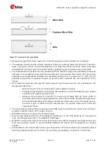
Figure 19 shows the design options and the main parameters to be considered when implementing a
transmission line on a PCB:
•
The micro strip (a track coupled to a single ground plane, separated by dielectric material)
•
The coplanar micro strip (a track coupled to the ground plane and side conductors, separated by
dielectric material)
•
The strip line (a track sandwiched between two parallel ground planes, separated by dielectric
material).

