background image


NINA-W1 series - System integration manual 

UBX-17005730 - R15 

System description


Page 12 of 54 

C1 - Public 


1.7.2.1


RMII Startup precautions  

The 

RMII_CLK

 input (GPIO27) is multiplexed with the ESP boot pin. Therefore, to ensure that the boot 

mode is not entered inadvertently, the 

RMII_CLK

 (GPIO27) must be held high during boot for at least 

1.5 ms. 

When using u-connectXpress, the 

RMII_CLK

  pin is monitored during boot. The u-connectXpress 

software checks the availability of the clock signal 1.2 s after boot. You must make sure to that the 

RMII_CLK

 signal is available at that time to enable the RMII interface. The clock signal can be enabled 

beforehand, but only if the requirement to avoid entering the ESP boot mode is not interfered with. 

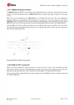
On  EVK-NINA-W1, these  startup precautions are  implemented using two buffers and a RC delay 
circuit that override the RMII clock from the PHY. This delays the clock so that it starts a short time 
(50 ms) after the module boot. 


Figure 4: EVK-NINA-W1 RMII clock delay circuit 


1.7.2.2


MAC to PHY connection 

When connecting NINA-W1 series  modules  to an external PHY circuit, both the RMII and SMI 
interfaces must be connected. The default PHY address (0x1) must be configured on the PHY side. 
Follow the recommendations of your chosen PHY chip supplier for implementation details.  

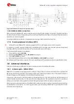
An example of a PHY implementation is shown in Figure 5. PHY KSZ8081 is recommended and is used 
on the EVK-NINA-W1.  

Summary of Contents for NINA-W1 Series

Page 1: ...les which includes the NINA W13 Wi Fi and NINA W10 and NINA W15 series multiradio modules These modules feature a number of useful embedded security features including secure boot that ensures that on...

Page 2: ...n NINA W102 Early Production Information NINA W106 Early Production Information NINA W131 Early Production Information NINA W132 Early Production Information NINA W151 Early Production Information NIN...

Page 3: ...Serial peripheral interface SPI 13 1 8 Antenna interfaces 13 1 8 1 Antenna pin NINA W1x1 13 1 8 2 NINA W1x2 and W1x6 integrated antennas 14 1 9 Reserved pins RSVD 14 1 10GND pins 14 Software 15 2 1 NI...

Page 4: ...for schematic design and PCB floor planning 39 3 5 2 Module placement 39 3 5 3 Layout and manufacturing 39 3 6 Module footprint and paste mask 39 3 7 Thermal guidelines 40 3 8 ESD guidelines 40 Handl...

Page 5: ...ocontroller MCU and radio for wireless communication With open CPU architecture NINA W10 series modules are ideal for advanced applications that run on dual core 32 bit MCUs The radio provides support...

Page 6: ...ulators RF ROM Wi Fi baseband IO buffers 2xXtensa 32 bit LX6 MCU SRAM 4Mbit Cryptographic hardware accelerations PIFA antenna NINA W132 PLL Quad SPI VCC_IO VCC 3 0 3 6 V 40 MHz Reset UART RMII EFUSE G...

Page 7: ...e configuration flash encryption and Chip ID Open CPU variants NINA W10 also support external FLASH and SRAM memory through a Quad SPI interface 1 4 Operating modes 1 4 1 Power modes NINA W1 series mo...

Page 8: ...te to avoid current leakage prior to the invocation of esp_deep_sleep_start void cbPWR_MGR_enterDeepSleep rtc_gpio_isolate GPIO_NUM_12 esp_deep_sleep_start The rtc_gpio_isolate function disables input...

Page 9: ...W1 series modules include an additional voltage supply input for setting the I O voltage level A separate VCC_IO pin enables module integration in many applications with different voltage supply level...

Page 10: ...ending on the intended use case for the module o On NINA W13 W15 modules pin 27 must be in default state during the boot o Care must be taken if an RMII interface is to be included in the application...

Page 11: ...ow control Table 2 UART port default settings It is recommended that the UART is either connected to a header for firmware upgrade or made available for test points The IO level of the UART follows VC...

Page 12: ...ock signal can be enabled beforehand but only if the requirement to avoid entering the ESP boot mode is not interfered with On EVK NINA W1 these startup precautions are implemented using two buffers a...

Page 13: ...tput Clock SPI_SCLK as input Optional hardware flow control lines SPI_NORX and SPI_DRDY as output For details on SPI operation see also the u connectXpress SPI peripheral protocol specification 10 1 8...

Page 14: ...in accordance with u blox reference designs Reference designs are available on request from u blox The designer integrating a u blox reference design into an end product is solely responsible for any...

Page 15: ...es capabilities and use of u connectXpress software see the u connectXpress AT commands manual 1 and u connectXpress user guide 6 Typical examples of the applications and use cases supported by NINA W...

Page 16: ...level APIs supported by the module chipset supplier The ESP IDF Software Development Kit is available from the Expressif website It bundles the Wi Fi stack and the broad range of drivers and librarie...

Page 17: ...e SoftDevice and ConnectivitySoftware applications Java Script Object Notation NINA W1XX CF version json For example NINA W15X CF 1 0 json ConnectivitySoftware NINA W10X SW x y z build bin For example...

Page 18: ...loader using either AT commands Pressing the SW1 and SW2 buttons simultaneously during a module reset initiated by setting RESET_N low For further information about the module reset see also the data...

Page 19: ...mission flags are marked in UNIX style rwx is the default flag for the u connectXpress software rw is the default flag for other binary images Table 3 Defined values for update parameters 2 4 1 2 1 Se...

Page 20: ...ommands to NINA W1 to execute tasks using open source terminal emulator software that supports XMODEM like TeraTerm or ExtraPuTTy Alternatively you can send all AT commands described in this section u...

Page 21: ...W1 displays the greeting text STARTUP Enter the Software version identification AT GMR command again to make sure that the latest software version is now installed 2 5 Developing and flashing NINA W1...

Page 22: ...environment Windows Linux Pip homebrew and other macros After installing the appropriate toolchain install ESP IDF using the Get ESP IDF instructions on the Espressif web site The toolchain for the E...

Page 23: ...the com port that is used to flash NINA W10 is modified 6 Exit the configuration window by pressing Q and confirm save the configuration Now the project is ready to build 7 Before building and flashi...

Page 24: ...table configuration for the project a custom partition scheme can also be set where addresses and data type are defined See also the Espressif Creating Custom Tables 16 2 5 5 Automatic bootloader on N...

Page 25: ...d correctly before downloading the Arduino files as mentioned in the next step The Arduino IDE user folder is typically located in C Users user_name Documents Arduino 2 6 2 Downloading from the GIT re...

Page 26: ...2 repository 2 6 3 Downloading the toolchain Go to the folder C Users user_name Documents Arduino hardware espressif esp32 tools to execute the program get exe Double click on the get exe to start the...

Page 27: ...rogram Files x86 Arduino arduino exe In the Tools Board menu select ESP32 Dev Module and then select the following Flash Mode DIO Flash Frequency 40 MHz Flash Size 2 MB 16 Mb Upload Speed 921600 Core...

Page 28: ...WiFiScan Press the arrow button as shown highlighted in red in the below screenshot Figure 16 to start the upload to NINA W10 Figure 16 Screenshot that depicts the arrow at the top Select Serial Moni...

Page 29: ...es at 6 dBm which is within the regulatory limit for NINA W1 2 7 1 3 Bluetooth low energy output power configuration No output power configuration for Bluetooth low energy is required Using the defaul...

Page 30: ...e and can affect compliance with regulatory standards for radiated emissions For schematic and layout design recommendations see also Antenna interface 12 System functions RESET_N GPIO and other Syste...

Page 31: ...o communication The NINA W1x2 and W1x6 modules with an internal surface mounted PIFA antenna or PCB trace antenna cannot be mounted in a metal enclosure No metal casing or plastics using metal flakes...

Page 32: ...e minimized to reduce dielectric losses o If traces longer than few centimeters are needed it is recommended to use a coaxial connector and cable to reduce losses o Stack up should allow for thick 50...

Page 33: ...es should carefully be selected with minimum insertion losses Additional insertion loss will be introduced by low quality or long cable Large insertion loss reduces radiation performance o A high qual...

Page 34: ...er to the power delivered to the antenna input the efficiency is a measure of how well an antenna receives or transmits Maximum Gain Refer to Data sheet The maximum antenna gain must not exceed the va...

Page 35: ...d user to replace the antenna with higher gain versions and exceed regulatory limits The following recommendations apply for proper layout of the connector Strictly follow the connector manufacturer s...

Page 36: ...etween co located RF systems like LTE sidebands on 2 4 GHz band Transmitted power may interact or disturb the performance of NINA W1 modules 3 3 3 On board antenna design If a plastic enclosure is use...

Page 37: ...GND plane underneath the entire module with a ground cut out under the PCB trace antenna according to the description in Figure 23 The NINA W1x6 has four extra GND pads under the antenna that need to...

Page 38: ...signals in the RMII bus with the same length and have appropriate grounding in the surrounding layers total bus length should also be minimized The layout of the RMII bus should be done so that crosst...

Page 39: ...imum signal skew for differential pairs and length matching of buses Minimize the routing length longer traces will degrade signal performance Ensure that maximum allowable length for high speed busse...

Page 40: ...vice implements an integral antenna the enclosure port is seen as all insulating and conductive surfaces housing the device If the device implements a removable antenna the antenna port can be separat...

Page 41: ...ghly automated process complies with the IEC61340 5 1 STM5 2 1999 Class M1 devices standard Consequently the designer should implement proper measures to protect from ESD events on any pin that may be...

Page 42: ...e first point of contact must always be to local GND Before mounting an antenna patch connect the device to ground When handling the RF pin do not touch any charged capacitors Be especially careful wh...

Page 43: ...used is dependent on the thermal mass of the entire populated PCB heat transfer efficiency of the oven and particular type of solder paste used The optimal soldering profile used has to be trimmed fo...

Page 44: ...soldered on it Boards with combined through hole technology THT components and surface mount technology SMT devices may require wave soldering to solder the THT components Only a single wave solderin...

Page 45: ...A W101 and NINA W102 FCC ID and IC certification number The u blox FCC ID and IC certification number for NINA W101 and NINA W102 is restricted and can be used only by u blox Integrators other than u...

Page 46: ...If the module is to be co located with another transmitter additional measurements for simultaneous transmission is required The results must be added to the grant file as a Class II Permissive Change...

Page 47: ...report for each unit can be generated Figure 26 shows the ATE typically used during u blox production u blox in line production testing includes Digital self tests firmware download MAC address progr...

Page 48: ...Device The standard operational module firmware and test software on the host can be used to perform functional tests communication with the host controller check interfaces and perform basic RF perfo...

Page 49: ...d DC Direct Current DC Direct Current DCE Data Circuit terminating Equipment Data Communication Equipment DDC Display Data Channel DDR Double Data Rate DL Down Link Reception DRX Discontinuous Recepti...

Page 50: ...dent Interface ROM Read only Memory RSSI Received Signal Strength Indicator RTC Real Time Clock SDK Software Development Kit SMA SubMiniature version A SMI Station Management Interface SPI Serial Peri...

Page 51: ...SDK Get Started 9 s center user guide UBX 16012261 10 u connectXpress SPI peripheral protocol specification UBX 20028725 11 u connectXpress bootloader protocol specification UBX 17065404 12 Espressif...

Page 52: ...d the Wi Fi output power configuration for NINA W10 series section 2 7 1 1 R06 6 Dec 2018 mwej fbro Added support for NINA W15 in many sections Added support for RMII Removed LPO clock support for NIN...

Page 53: ...Added time window of availability of RMII_CLK during boot Section 2 4 Module re programming via UART requirement added R15 27 Oct 2021 ldas lkis Changed document status for NINA W156 to Early Product...

Page 54: ...com Regional Office China Beijing Phone 86 10 68 133 545 E mail info_cn u blox com Support support_cn u blox com Regional Office China Chongqing Phone 86 23 6815 1588 E mail info_cn u blox com Suppor...

Reviews: