background image

5

ANTENNA

5 Antenna

5.1 Antenna type

WBR1D-IPEX uses only an Ipex antenna.

5.2 Antenna interference reduction

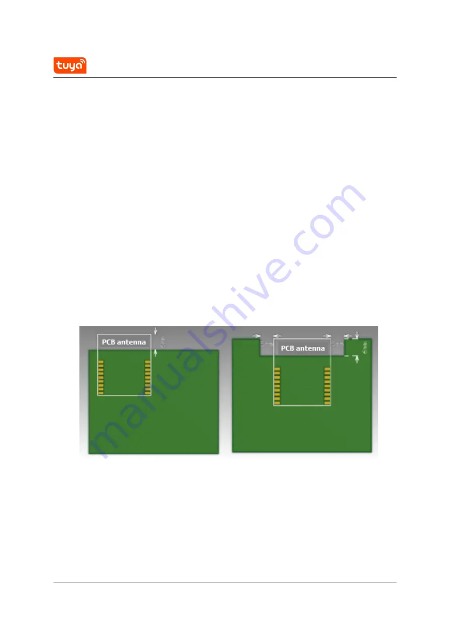
To ensure the optimal WiFi performance when the WiFi module uses an onboard PCB

antenna, it is recommended that the antenna be at least 15 mm away from other
metal parts.

To ensure the antenna performance, the PCB should not be routed or clad with cop-

per in the antenna area. The main points of the layout: 1. Make sure that there is
no substrate medium directly below or above the printed antenna. 2. Make sure
that the area around the printed antenna is far away from the metal copper skin, so
as to ensure the radiation effect of the antenna to the greatest extent.

For the antenna area of the PCB of the module, refer to Diagram of Mechanical
Dimensions.

16 / 29

Summary of Contents for WBR1D-IPEX

Page 1: ...WBR1D IPEX Module Datasheet Hardware Product Development Network Modules Wi Fi BLE Dual Mode Module WBR Series Module Version 20210329 Online Version...

Page 2: ...ditions 9 3 3 TX and RX power consumption 10 3 4 Working current 11 4 RF parameters 13 4 1 Basic RF features 13 4 2 TX performance 13 4 3 RX performance 15 5 Antenna 16 5 1 Antenna type 16 5 2 Antenna...

Page 3: ...ntents 7 4 The Diagram of PCB package 21 7 5 Production instructions 22 7 6 Recommended oven temperature curve 24 7 7 Storage conditions 26 8 MOQ and packaging information 27 9 Appendix Statement 27 i...

Page 4: ...embedded Wi Fi module that Tuya has developed It consists of a highly integrated wireless RF chip W701D VA1 CG a few peripherals a built in WiFi network protocol stack the Bluetooth network protocol...

Page 5: ...block diagram of WBR1D IPEX is shown as below 1 1 Features Embedded low power 32 bit CPU which can also function as an application processor The maximum clock rate 200 MHz Working voltage 3 3 0 3V Pe...

Page 6: ...9 dBm output power PCB antenna with a gain of 2 dBi 2 4 G which is shared by Wi Fi and Bluetooth Working temperature 20 to 85 1 2 Applications Intelligent building Smart household and home appliances...

Page 7: ...FACES 2 Module interfaces 2 1 Dimensions and footprint WBR1D IPEX has two rows of pins with a 1 5 0 1 mm pin spacing The WBR1D IPEX dimensions are 18 mm W 23 5 mm L 2 8 mm H Diagram of dimensions of W...

Page 8: ...E INTERFACES Note The general shape tolerance is 0 3 mm the position tolerance related to the plug in assembly is reduced to 0 1 mm and the tolerance of the 1 mm thick plate is 0 1 mm 2 2 Pin definiti...

Page 9: ...PB1 I O User side serial interface TXD signal 3 RX PB2 I O User side serial interface RXD signal 4 3V3 P Power supply pin 3 3V 5 GND P Power supply reference ground 6 PA12 I O Support hardware PWM fun...

Page 10: ...al interface input pin 12 PB21 I O Common IO pin which corresponds to PB 21 of IC 13 PA25 I O Support hardware PWM function and correspond to PA 25 of IC 14 GND P Power supply reference ground 15 GND...

Page 11: ...y a hardware reset pin and cannot be used for clearing information about WiFi network con guration 2 3 Definitions on test points Pin aq Symbol I O type Function TEST I Be used for the production test...

Page 12: ...ature 20 85 VBAT Power supply voltage 3 0 3 6 V Static electricity discharge voltage human body model TAMB 25 2 KV Static electricity discharge voltage machine model TAMB 25 0 5 KV 3 2 Normal working...

Page 13: ...output VCC 0 8 VCC V Imax IO drive current 12 mA 3 3 TX and RX power consumption 3 3 1 Transmission and receiving at 2 4G Working Status Mode Rate Transmit Power Re ceive Typical value Unit Transmit 1...

Page 14: ...3 mA 3 3 2 Transmission and receiving at 5G Working Status Mode Rate Transmit Power Re ceive Typical value Unit Transmit 11a 54Mbps 15dBm 300 mA Transmit 11n HT20 MCS7 15dBm 230 mA Transmit 11n HT40 M...

Page 15: ...ule is in the fast network connection state and the WiFi indicator ashes fast 57 184 mA Hotspot network con gura tion state The module is in the hotspot network con gura tion state and the WiFi indica...

Page 16: ...sic RF features Parameter Description Working frequency 2 412 to 2 484 GHz 5 180 to 5 885 GHz WiFi standard IEEE 802 11 a b g n Channels 1 to 14 channels 36 to 177 Data transmission rate 11b 1 2 5 5 1...

Page 17: ...m Average RF output power 802 11g OFDM Mode 54M 16 dBm Average RF output power 802 11n HT20 Mode MCS7 15 dBm Average RF output power 802 11n HT40 Mode MCS7 14 dBm Frequency error 10 10 ppm 5G TX Perfo...

Page 18: ...ge RF output power 802 11n HT40 Mode MCS7 12 dBm Frequency error 10 10 ppm 4 3 RX performance RX sensitivity Parameter Minimum value Typical value Maximum value Unit PER 8 RX sensitivity 802 11b DSSS...

Page 19: ...ensure the antenna performance the PCB should not be routed or clad with cop per in the antenna area The main points of the layout 1 Make sure that there is no substrate medium directly below or above...

Page 20: ...3 3V within 40mS Symbol Parameter Minimum Typical Maximum Unit TPRDY 3 3V ready time 0 6 40 mS CHIP_EN CHIP_EN ready time 0 6 40 mS 6 2 Resetting When designing a plate of a module you should reserve...

Page 21: ...tor at an output port of a pin and then connect a diode in series In this case the voltage of a GPIO will drop to about 2 7V after passing through the diode The red box represents the original drive t...

Page 22: ...6 POWER ON SEQUENCE AND RESETTING 19 29...

Page 23: ...7 PACKAGING INFORMATION AND PRODUCTION INSTRUCTIONS 7 Packaging information and production instructions 7 1 Mechanical dimensions The PCB dimensions are 18 mm W 23 5 mm L 2 8 mm H 7 2 Side view 20 29...

Page 24: ...te The default dimensional tolerance is 0 35 mm If you have speci c requirements on dimensions make them clear in the datasheet after communi cation 7 3 Schematic diagram of packaging 7 4 The Diagram...

Page 25: ...ed it must be soldered within 24 hours Otherwise it must be put into the drying cupboard where the RH is not greater than 10 or it needs to be packaged under vacuum again and the exposure time needs t...

Page 26: ...the vacuum packing bag After being unpacked 10 and above circles on the HIC become pink The total exposure time has been more than 168 hours since unpacking More than 12 months have passed since the s...

Page 27: ...ischarge ESD protective measures To guarantee the passing rate it is recommended that you use the SPI and AOI to monitor the quality of solder paste printing and mounting 7 6 Recommended oven temperat...

Page 28: ...perature 150 to 200 C F Duration above the liquidus 50 to 70s G Peak temperature 235 to 245 C H Ramp down slope 1 to 4 C s Note The above curve is just an example of the solder paste SAC305 For more d...

Page 29: ...7 PACKAGING INFORMATION AND PRODUCTION INSTRUCTIONS 7 7 Storage conditions 26 29...

Page 30: ...e designed to provide reasonable protection against harmful interference in a residential instal lation This device generates uses and can radiate radio frequency energy and if not installed and used...

Page 31: ...lar transmitter installed The end user manual shall include all required regulatory information warnings as shown in this manual including This product must be installed and operated with a minimum di...

Page 32: ...ust not be disposed of as normal household waste in accordance with the EU directive for waste electrical and electronic equipment WEEE 2012 19 EU Instead it should be disposed of by returning it to t...

Reviews: