background image

TE0712 TRM 

Revision: V14 

Copyright © 2017 Trenz Electronic GmbH

Page 

 of 

12

20

http://www.trenz-electronic.de

Power Rails

Power Rail 

Name

B2B Connector 

JM1 Pin

B2B Connector 

JM2 Pin

Direction

Notes

VIN

1, 3, 5

2, 4, 6, 8

Input

SoM supply voltage (from the baseboard).

3.3VIN

13, 15

-

Input

SoM supply voltage (from the baseboard).

1.5V

-

19

Output

Module internal 1.5V level.

1.8V

39

-

Output

Module internal 1.8V level. Maximum 300mA available.

3.3V

14

10, 12

Output

Module internal 3.3V level.

VCCIO13

-

1, 3

Input

High-Range bank supply voltage (from the baseboard).

VCCIO15

-

7, 9

Input

High-Range bank supply voltage (from the baseboard).

VCCIO16

9, 11

-

Input

High-Range bank supply voltage (from the baseboard).

VREF_JTAG

-

91

Output

JTAG reference voltage (3.3V).

Summary of Contents for TE0712 TRM

Page 1: ...TE0712 TRM Date Revision V14 07 Jun 2017 19 08 ...

Page 2: ...________________ 11 Power On Sequence _________________________________________________________________ 11 Power Rails ________________________________________________________________________ 12 Board to Board Connectors _____________________________________________________________ 13 Connector Mechanical Ratings _________________________________________________________ 13 Manufacturer Documentati...

Page 3: ...15T to 200T supported by the free software Xilinx Vivado WebPACK Both industrial and commercial temperature ranges available Rugged for high shock resistance and high vibration 1 GByte DDR3 32 bit SDRAM 10 100 Mbit Ethernet PHY MAC address EEPROM 32 MByte QSPI Flash memory with XiP support Programmable clock generator Transceiver clock default 125 MHz Fabric clock default 200 MHz Plug on module wi...

Page 4: ...TE0712 TRM Revision V14 Copyright 2017 Trenz Electronic GmbH Page of 4 20 http www trenz electronic de Block Diagram ...

Page 5: ...stem Controller CPLD Lattice Semiconductor MachXO2 256HC U3 4 Gbit DDR3 SDRAM Intelligent Memory IM4G16D3EABG U19 Serial EEPROM Microchip 11AA02E48 U7 M2 Samtec Razor Beam LSHM 150 J B2B connector M1 Samtec Razor Beam LSHM 150 J B2B connector M3 Samtec Razor Beam LSHM 150 J B2B connector 12A Enpirion EN63A0QI PowerSoC DC DC converter U14 Green LED SYSLED1 D1 Red LED SYSLED2 D2 Initial Delivery Sta...

Page 6: ...14 JM1 8 3 3V 14 JM2 18 3 3V 14 JM3 4 3 3V 15 JM2 48 VCCIO15 Supplied by the baseboard 15 JM2 2 VCCIO15 Supplied by the baseboard 16 JM1 48 VCCIO16 Supplied by the baseboard Please refer to the tables page for additional information Pin out JTAG Interface JTAG access to the Xilinx Artix 7 FPGA and System Controller CPLD devices is provided through B2B connector JM2 JTAG Signal B2B Pin TMS JM2 93 T...

Page 7: ...mal operation high for System Controller CPLD access EN1 Input Power Enable When forced low pulls POR_B low to emulate power on reset NOSEQ No function Not used MODE No function Not used Pin usages depends on CPLD Firmware see TE0712 CPLD On board LEDs The TE0712 module has 2 LEDs which are connected to the System Controller CPLD Once FPGA configuration has completed these can be used by the user ...

Page 8: ...FPGA master and clock generator slave 2 Proper logic needs to be created in the FPGA to exercise the I C bus with the correct data See the 2 reference design section for more information CLK Output FPGA Bank FPGA Pin IO Standard Net Name Default Frequency Notes CLK0 34 K4 J4 DIFF_SSTL15 CLK0_P N NB Since PCB REV02 CLK1A CLK50M 50 MHz PHY chip RMII reference clock CLK1B 34 R4 CLK50M2 NB Since PCB R...

Page 9: ...l FPGA configuration process The FPGA is held in reset by driving the PROG_B signal low until all power supplies have stabilized By driving signal RESIN to low you can reset the FPGA This signal can be driven from the user s baseboard PCB via the B2B connector JM2 pin 18 Input EN1 is also gated to FPGA reset should be open or pulled up for normal operation By driving EN1 low on board DC DC convert...

Page 10: ...t data 0 Output to Ethernet PHY P15 ETH_TX_D1 Ethernet transmit data 1 Output to Ethernet PHY R14 ETH_TX_EN Ethernet transmit enable N13 ETH_RX_D0 Ethernet receive data 0 Input from Ethernet PHY N14 ETH_RX_D1 Ethernet receive data 0 Input from Ethernet PHY P20 ETH_RX_DV Ethernet receive data valid All signals are connected to the FPGA bank 14 and correspond to LVCMOS33 standard MAC Address EEPROM ...

Page 11: ...onsumption and heat dissipation will rise due to the DC DC converter efficiency it decreases when VIN VOUT ratio rises Power On Sequence For the highest efficiency of the on board DC DC regulators it is recommended to use same 3 3V power source for both VIN and 3 3VIN power rails Although VIN and 3 3VIN can be powered up in any order it is recommended to power them up simultaneously It is importan...

Page 12: ...N 13 15 Input SoM supply voltage from the baseboard 1 5V 19 Output Module internal 1 5V level 1 8V 39 Output Module internal 1 8V level Maximum 300mA available 3 3V 14 10 12 Output Module internal 3 3V level VCCIO13 1 3 Input High Range bank supply voltage from the baseboard VCCIO15 7 9 Input High Range bank supply voltage from the baseboard VCCIO16 9 11 Input High Range bank supply voltage from t...

Page 13: ...seboard compatible to Mating height REF 189016 01 LSHM 150 02 5 L DV A S K TR 6 5 mm LSHM 150 03 0 L DV A S K TR LSHM 150 03 0 L DV A S K TR 7 0 mm REF 189016 02 LSHM 150 04 0 L DV A S K TR 8 0 mm LSHM 150 06 0 L DV A S K TR LSHM 150 06 0 L DV A S K TR 10 0mm REF 189017 01 LSHM 130 02 5 L DV A S K TR 6 5 mm LSHM 130 03 0 L DV A S K TR LSHM 130 03 0 L DV A S K TR 7 0 mm REF 189017 02 LSHM 130 04 0 ...

Page 14: ...2013 11 28 16 54 LSHM 1XX XX X XX DV A X X TR MKT pdf 1 2013 11 28 16 56 REF 189016 01 pdf 1 2015 10 30 11 54 REF 189016 02 pdf 1 2015 10 30 11 54 REF 189017 01 pdf 1 2015 10 30 11 54 REF 189017 02 pdf 1 2015 10 30 11 54 TC0923 2523_report_Rev_2_qua pdf 1 2013 11 28 16 55 hsc report_lshm lshm 05mm_web pdf 1 2013 11 28 16 56 lshm_dv pdf 1 2013 11 28 16 56 tc0929 2611_qua 1 pdf 1 2013 11 28 16 55 ...

Page 15: ...85 C Industrial grade 4 0 mm TE0712 02 200 1I XC7A200T 1FBG484I 40 C to 85 C Industrial grade 4 0 mm TE0712 02 200 2I XC7A200T 2FBG484I 40 C to 85 C Industrial grade 4 0 mm TE0712 02 200 1I3 XC7A200T 1FBG484I 40 C to 85 C Industrial grade 2 5 mm TE0712 02 100 2C XC7A100T 2FGG484C 0 C to 85 C Commercial grade 4 0 mm TE0712 02 100 2C3 XC7A100T 2FGG484C 0 C to 85 C Commercial grade 2 5 mm TE0712 02 2...

Page 16: ...26 V Xilinx datasheet DS181 Storage temperature 55 100 C See IM4G16D3EABG datasheet Recommended Operating Conditions Parameter Min Max Units Reference Document VIN supply voltage 2 4 5 5 V EP53F8QI datasheet 3 3VIN supply voltage 2 9 5 5 V TPS748 datasheet HR I O banks supply voltage VCCO 1 14 3 465 V Xilinx datasheet DS181 HR I O banks input voltage 0 20 VCCO 0 2 V Xilinx datasheet DS181 Operatin...

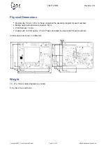
Page 17: ... size 50 mm 40 mm Please download the assembly diagram for exact numbers Mating height with standard connectors 8mm PCB thickness 1 6mm Highest part on PCB approx 2 5mm Please download the step model for exact numbers All dimensions are shown in millimeters Weight 16 27 g Plain module depends on variant 8 8 g Set of nuts and bolts ...

Page 18: ...n number is printed on the PCB board together with the module model number separated by the dash Document Change History Date Revision Contributors Description 2017 05 29 V14 Jan Kumann Variants table added Key Features section relocated 2017 03 01 V3 2 John Hartfiel BUGFIX in the description of System Controller I O section 2017 03 01 v3 1 John Hartfiel Update Clocking Section 2017 01 26 V3 Jan K...

Page 19: ...tation those resulting from lost profits lost data or business interruption arising out of the use inability to use or the results of use of this document any documents linked to this document or the materials or information contained at any or all such documents If your use of the materials or information from this document results in the need for servicing repair or correction of equipment or da...

Page 20: ...Directive 2002 96 EC of the European Parliament and of the Council of 27 January 2003 on waste electrical and electronic equipment WEEE Users of electrical and electronic equipment in private households are required not to dispose of waste electrical and electronic equipment as unsorted municipal waste and to collect such waste electrical and electronic equipment separately By the 13 August 2005 M...

Reviews: