Transmeta Crusoe TM5500 System Design Manual Download Page 114

July 17, 2002

114

PCB Layout Guidelines

7.3.3 Allegro Extended Spacing Constraints 
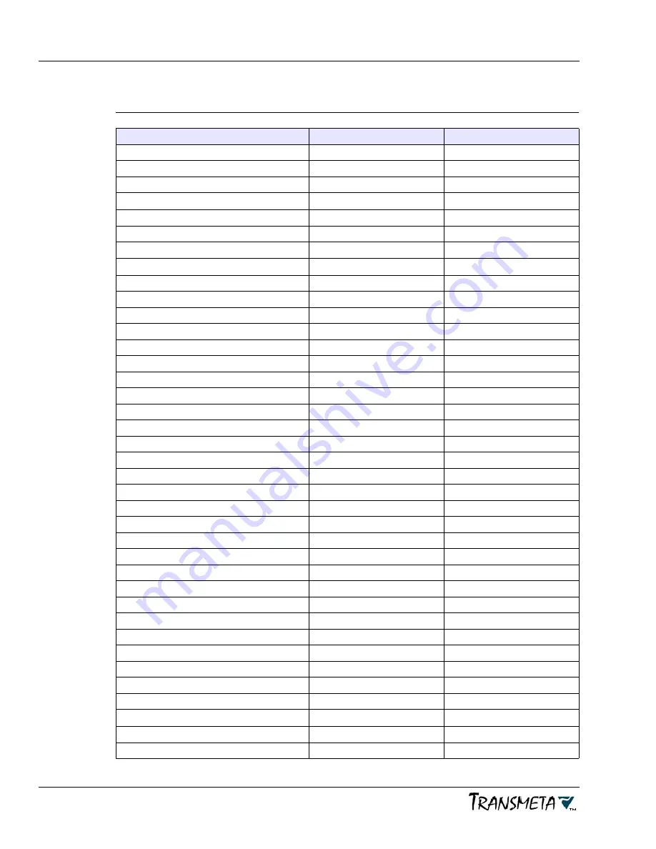
Table 19:

Extended Global Spacing/Line/Via Constraints 

1


Constraint Name

Default Constraint Value

BGA Constraint Value

Pin-to-pin

5 mils

5 mils

Line-to-pin

5 mils

5 mils

Line-to-line

5 mils

5 mils

Via-to-pin

Note 

2

Note 

2

Via-to-via

10 mils

10 mils

Via-to-line

5 mils

5 mils

Shape-to-pin

5 mils

5 mils

Shape-to-via

5 mils

Note 

2

Shape-to-line

5 mils

5 mils

Shape-to-shape

5 mils

5 mils

Thru pin-to-thru pin

5 mils

5 mils

Thru pin-to-SMD pin

5 mils

5 mils

Thru pin-to-test pin

5 mils

5 mils

Thru pin-to-thru via

10 mils

6 mils

Thru pin-to-test via

10 mils

6 mils

Thru pin-to-buried blind via

10 mils

6 mils

Thru pin-to-line

5 mils

5 mils

Thru pin-to-shape

5 mils

5 mils

SMD pin-to-SMD pin

5 mils

5 mils

SMD pin-to-test pin

5 mils

5 mils

SMD pin-to-thru via

8 mils

7 mils

SMD pin-to-test

8 mils

7 mils

SMD pin-to-buried blind via

8 mils

7 mils

SMD pin-to-line

5 mils

5 mils

SMD pin-to-shape

5 mils

5 mils

Test pin-to-test pin

5 mils

5 mils

Test pin-to-thru via

10 mils

6 mils

Test pin-to-test via

10 mils

6 mils

Test pin-to-buried blind via

10 mils

6 mils

Test pin-to-line

5 mils

5 mils

Test pin-to-shape

5 mils

5 mils

Thru via-to-thru via

10 mils

10 mils

Thru via-to-test via

10 mils

10 mils

Thru via-to-buried blind via

10 mils

10 mils

Thru via-to-line

5 mils

5 mils

Thru via-to-shape

5 mils

Note 

2

Test via-to-test via

10 mils

10 mils

Test via-to-buried blind via

10 mils

10 mils

Summary of Contents for Crusoe TM5500

Page 1: ...TM5500 TM5800 System Design Guide July 17 2002...

Page 2: ...without notice Transmeta products have not been designed tested or manufactured for use in any application where failure malfunction or inaccuracy carries a risk of death bodily injury or damage to t...

Page 3: ...ore Power Supply Example 25 3 1 3 PLL Power Supply 30 3 1 4 I O Power Supplies 33 3 1 5 Decoupling Capacitors 34 3 2 Power Supply Sequencing 35 3 2 1 Power Sequencing Requirements 35 3 2 2 Power Seque...

Page 4: ...h ROM Write Protection Circuit 93 6 5 3 Combined BIOS CMS Parallel ROM Interface 96 6 6 Southbridge 98 6 6 1 Qualified Southbridge Devices 98 6 6 2 Using CLKRUN 98 6 6 3 Southbridge Schematics 98 6 7...

Page 5: ...put Control Selector 25 Table 9 MAX1718 DSX Voltage Configuration 26 Table 10 Power Supply Sequencing Timing Specifications 35 Table 11 DDR SDRAM Memory Configurations 51 Table 12 SDR SDRAM Memory Con...

Page 6: ...July 17 2002 6 List of Tables...

Page 7: ...m Layer 58 Figure 10 Physical SDRAM Configurations 68 Figure 11 Read Timing Compensation 70 Figure 12 Adjustment of CLKIN Delay 71 Figure 13 Optimum Placement and Routing 72 Figure 14 Sub optimal Plac...

Page 8: ...July 17 2002 8 List of Figures...

Page 9: ...R SDRAM memory into a design Chapter 5 SDR Memory Design provides design guidelines and layout requirements for incorporating SDR SDRAM memory into a design Chapter 6 System Design Considerations desc...

Page 10: ...signal names used in the Data Book and other hardware specific materials can be different from those used on the reference schematics This section shows the terms used in the System Design Guide and...

Page 11: ...iption C0 Normal Active power state with processor executing instructions C1 Auto Halt Sleep state entered by processor executing HALT instruction C2 Quick Start Sleep state requiring chipset hardware...

Page 12: ...ventions used in the schematics S4 Suspend to Disk STD Current processor state is suspended and saved to non volatile disk All power supplies except _ALWAYS are off S5 Soft Off System is turned off Al...

Page 13: ..._IRDY PCI_LOCK PCI_PAR CPU_RST CLK_PCI_TM PCI_PERR PCI_STOP PCI_TRDY PCI_REQ 5 0 PCI_SERR SUSC SUSB PWRGOOD PCI_FERR CPU_IGNNE INIT INTR NMI SMI CPU_CLK CPU_STPCLK SUSPEND PCI_RST CPU_RST SYS_RST conn...

Page 14: ...translator Isolation Signal isolation is used to ensure that CKE signals to the SDRAMs remain stable during processor power transitions Since the processor does not have a suspend power well output si...

Page 15: ...July 17 2002 15 Example System Block Diagram and Schematics 2 2 Processor Schematics The following pages show TM5500 TM5800 processor reference schematics...

Page 16: ...0 DDR_BA1 DDR_CAS DDR_DQS 7 0 DDR_A 12 0 DDR_CS2 DDR_CKE_MUX0 CLK_DDRA DDR_CS1 DDR_CS0 DDR_MWE DDR_CKE_MUX1 CLK_DDRB DDR_DQM 7 0 DDR_CS3 V2_5 RN12A 24 1 8 RN17B 24 2 7 RN1A 10 1 8 RN7C 24 3 6 RN22C 24...

Page 17: ...Q61 SDR_DQ18 SDR_A0 SDR_DQ1 SDR_CS1 SDR_DQ56 SDR_DQM2 SDR_CKE_MUX0 SDR_DQ29 SDR_A8 SDR_DQ16 SDR_DQ5 SDR_DQ19 SDR_DQ28 SDR_DQ10 SDR_A2 SDR_DQ13 SDR_CS0 SDR_A10 SDR_DQ6 SDR_CKE_MUX1 SDR_BA1 SDR_A3 SDR_A...

Page 18: ...UN PCI_GNT1 PCI_DEVSEL PCI_STOP PCI_REQ0 PCI_REQ5 PCI_REQ4 PCI_REQ1 PCI_REQ2 PCI_REQ3 PCI_HLD V3_3 V3_3 V3_3 V3_3 V3_3 V3_3 R 10K 1 2 RN50C 10K 3 6 RN54C 10K 3 6 RN52D 10K 4 5 RN51B 10K 2 7 RN51C 10K...

Page 19: ...NT PWRGOOD SROM_CS0 CLK_CPU EPROMA1 SROM_SIN CPU_INIT SROM_SCLK TDM_TMS CPU_STPCLK DIODE_CATHODE SRCLK CPU_IGNNE TDM_SROM_CS1 CPU_FERR TDM_TRST DEBUG_INT CPU_SMI TDM_TCK TDM_SDA TDM_TDO TDM_RST DIODE_...

Page 20: ...OVDD IOVDD IOVDD IOVDD IOVDD IOVDD IOVDD IOVDD IOVDD IOVDD IOVDD IOVDD IOVDD IOVDD IOVDD IOVDD IOVDD IOVDD IOVDD IOVDD IOVDD IOVDD IOVDD IOVDD IOVDD IOVDD IOVDD IOVDD IOVDD25 IOVDD25 IOVDD25 IOVDD25 I...

Page 21: ...2 System Block Diagram shows the power supplies for each of the major components The power source for all notebook computers is either a battery 20 V or a DC wall adapter of a comparable voltage An in...

Page 22: ...UST NOT EXCEED 1 5 V OR PERMANENT DEVICE DAMAGE MAY RESULT Table 5 Core Power Supply Requirements for TM5500 TM5800 Processors Specification Value Notes Core voltage range 0 95 1 30 V nominal See Long...

Page 23: ...bulk capacitors 5 m maximum Combined capacitance of bulk capacitors 800 F minimum nominal 1100 F maximum nominal Distribution resistance from bulk capacitors to processor 2 m maximum Inductor inductan...

Page 24: ...0 1 0x05 1 50 V 0 0 1 1 0 0x06 1 45 V 0 0 1 1 1 0x07 1 40 V 0 1 0 0 0 0x08 1 35 V 0 1 0 0 1 0x09 1 30 V 0 1 0 1 0 0x0A 1 25 V 0 1 0 1 1 0x0B 1 20 V 0 1 1 0 0 0x0C 1 15 V 0 1 1 0 1 0x0D 1 10 V 0 1 1 1...

Page 25: ...used to control the output voltage is determined by the ZMODE and SUS input signals These inputs control internal multiplexers that select which register is presented to the DAC to set the output vol...

Page 26: ...to the TM5500 TM5800 processor core during extended Deep Sleep periods significantly reducing processor leakage power during long intervals of sustained system inactivity The reference design example...

Page 27: ...n the output voltage which in the reference design example is approximately 0 85 See the MAX1718 data sheet for detailed information on adjusting the output voltage offset 3 1 2 5 Switching Frequency...

Page 28: ...ing up as required by TM5500 TM5800 power sequencing specifications VGATE has an internal sense circuit to force it high during programmed transitions such as normal LongRun voltage step transitions w...

Page 29: ...ionofTransmeta Corporation It is nottobedisclosedorused except inaccordancewithapplicable agreements Thiscopyrightnoticedoesnot evidenceanyactualorintendedpublicationof suchdocument Page of Title Docu...

Page 30: ...t 1 0 V 50 mV across a nominal core operating voltage range of 0 9 V to 1 0 V For transitions in the core voltage e g during LongRun power management voltage steps V_CPU_PLL must settle to within the...

Page 31: ...rved This documentcontainsconfidentialand proprietaryinformationofTransmeta Corporation It is nottobedisclosedorused except inaccordancewithapplicable agreements Thiscopyrightnoticedoesnot evidenceany...

Page 32: ...to the processor V_CPU_PLL pin as possible and the V_CPU_PLL GND loop length should be minimized Circuit Operation During operation the V5_0 5 0 V supply to the opamp and V2_5 2 5 V supply to Q1 must...

Page 33: ...es are derived from V3_3_STR and V2_5_STR care must be taken to ensure the voltages are not glitched when these supplies are turned on Glitching can be minimized by controlling the turn on rise time o...

Page 34: ...er peripheral decoupling capacitors V_CPU_CORE Underside BGA Decoupling Example BOTTOM SIDE AS SEEN FROM TOP SIDE SHARED VIA TO GND Y10 W10 SHARED VIA TO V_CPU_CORE V11 U10 SHARED VIA TO GND U9 T10 SH...

Page 35: ...in the figure below System designs for TM5500 TM5800 processors must also meet the power on requirements specified in the Data Book The table below provides timing specifications for the power supply...

Page 36: ...ch off The current spike may trigger other system level protection circuits or result in I O contention 3 2 2 Power Sequencing Circuit Examples As explained above in Power Sequencing Requirements on p...

Page 37: ...poration All rightsreserved This documentcontainsconfidentialand proprietaryinformationofTransmeta Corporation It is nottobedisclosedorused except inaccordancewithapplicable agreements Thiscopyrightno...

Page 38: ...July 17 2002 38 Processor Power Supplies and Power Management 3 3 Power Supply Voltage Supervisor The following page shows a power supply voltage supervisor reference design schematic...

Page 39: ...tcontainsconfidentialand proprietaryinformationofTransmeta Corporation It is nottobedisclosedorused except inaccordancewithapplicable agreements Thiscopyrightnoticedoesnot evidenceanyactualorintendedp...

Page 40: ...July 17 2002 40 Processor Power Supplies and Power Management 3 4 POWERGOOD Block Diagram Example The following page shows an example block diagram for possible system POWERGOOD circuits...

Page 41: ...E SYSTEM LEVEL POWERGOOD TO THE TM5800 CPU AND SOUTHBRIDGE NOTE ENABLE_VIO MANUAL_RST WHEN ENABLE_VIO MANUAL_RST IS HIGH THE CORE VOLTAGE IS AT LEVEL ENABLE_VIO IS THEN USED WITH THE VOLTAGE SEQUENCIN...

Page 42: ...r the power on sequence are provided here Parameter Description Min Max Diagram Note tvdd_rise Supply delay and rise time 1 1 Refer to Figure 4 and Table 10 for details on power supply sequencing timi...

Page 43: ...of the notes in the diagrams below Refer to Figure 4 and Table 10 for details on power supply sequencing timing Power On C0 PCI_RST RESET POWERGOOD CPU_CLK PCI_CLK V_CPU_CORE V_CPU_PLL V3_3 V2_5 T1 T2...

Page 44: ...O cycle that initiates the C3 power state is typically snooped by the processor The processor integrated northbridge must be properly configured to snoop this I O cycle and the power management softwa...

Page 45: ...C0 3 S typical 5 S maximum T7 State Transition Timing Information Requirements Diagram Note STPCLK assertion to Stop Grant cycle 3 5 S typical 8 S maximum T1 Stop Grant to SLEEP assertion 2 S minimum...

Page 46: ...Ms into self refresh by the time the I O cycle reaches the power management controller There are no special requirements for the power management signaling between the I O cycle and the removal of mai...

Page 47: ...ntroller waits 64 S between de asserting the processor SLEEP signal and de asserting the processor STPCLK signal This type of system is expected to have a worst case C3 entrance exit latency of 207 S...

Page 48: ...rt by ensuring that there is no external activity in the system during the frequency change This is accomplished by flushing any queued PCI or memory writes and force granting the PCI bus to the proce...

Page 49: ...to account for the regulator settling time The default LongRun power management parameters assume a 64 S settling time which is compatible with the voltage regulators referenced in this document Note...

Page 50: ...July 17 2002 50 Processor Power Supplies and Power Management...

Page 51: ...ce The DDR SDRAM controller supports the equivalent of one DIMM one bank only of DDR SDRAM using a 64 bit wide interface The DDR SDRAM interface does not support parity bits The DDR SDRAM can be popul...

Page 52: ...ter of the Development and Manufacturing Guide for further LongRun configuration and memory frequency information 4 2 Clock Enable Isolation The processor DDR_CKE clock enable signals must be isolated...

Page 53: ...d 2490 For a DDR_VREF specification of 1 35 V the recommended V2_5 voltage divider network for deriving DDR_VREF is upper resistor tied to V2_5 1960 and lower resistor tied to ground 2320 4 4 1 DDR Re...

Page 54: ...ed such that the maximum difference in their lengths is 0 4 or less The DDR_DQS signal for the group must have a length that is within 0 1 of the longest other trace in that group The length of all DQ...

Page 55: ...device placement using both sides of the PCB Figure 6 Recommended 4 Device DDR Memory Chip Placement DDR 2 DDR 3 DDR 0 TM5x00 Processor DDR 1 Top Bottom Place components one over the other on opposit...

Page 56: ...ide Top Layer Signal Routing The figure below shows the connections from the TM5500 TM5800 processor to the DDR memory on the primary top layer side of the board Figure 7 Recommended 4 Device DDR Memo...

Page 57: ...sign Internal Layer Signal Routing The figure below shows the connections from the TM5500 TM5800 processor to the DDR memory on an internal layer of the board Figure 8 Recommended 4 Device DDR Memory...

Page 58: ...Bottom Layer Signal Routing The figure below shows connections from the TM5500 TM5800 processor to the DDR memory on the secondary bottom layer side of the board Figure 9 Recommended 4 Device DDR Mem...

Page 59: ...59 DDR Memory Design 4 7 DDR SDRAM Schematics The following pages show DDR SDRAM reference schematics Single bank DDR soldered down 2 pages Single bank DDR SODIMM 2 pages DDR clock enable isolation ci...

Page 60: ...DQ17 DDR_DQ7 DDR_DQS3 DDR_A10 DDR_A7 DDR_DQ30 DDR_DQ31 DDR_A0 DDR_DQ20 DDR_CS0 DDR_DQ16 DDR_MWE DDR_A7 DDR_DQ19 DDR_A10 CLK_DDRA DDR_A2 DDR_BA0 DDR_DQ 63 0 DDR_A 12 0 CLK_DDRA DDR_RAS DDR_DQM 7 0 DDR_...

Page 61: ...DR_A0 DDR_A8 CLK_DDRB DDR_DQ34 DDR_CS0 DDR_A2 DDR_RAS DDR_RAS DDR_DQ57 DDR_DQ52 DDR_A 12 0 DDR_DQ 63 0 DDR_DQS 7 0 DDR_BA0 DDR_CS0 DDR_CKE0 DDR_RAS CLK_DDRB DDR_CAS DDR_MWE DDR_DQM 7 0 DDRVREF DDR_BA1...

Page 62: ...DDR_A8 DDR_DQS6 DDR_DQ16 DDR_DQ10 DDR_DQ24 DDR_DQ0 DDR_DQM6 DDR_DQ11 DDR_DQ3 DDR_DQ47 DDR_DQ42 DDR_DQ12 DDR_A10 DDR_CS0 DDR_DQ 63 0 DDR_CKE1 DDR_CS1 CLK_DDRA DDR_DQS 7 0 CLK_DDRA CLK_DDRB SMBCLK DDR_R...

Page 63: ...1 2 C9 0 1uF 1 2 C3 0 1uF 1 2 J1B 200_SODIMM_DDR 197 199 1 2 3 4 15 16 27 28 38 39 40 51 52 63 64 75 76 87 88 90 103 104 125 126 137 138 149 150 159 161 162 173 174 185 186 9 10 21 22 33 34 36 45 46 5...

Page 64: ...pt inaccordancewithapplicable agreements Thiscopyrightnoticedoesnot evidenceanyactualorintendedpublicationof suchdocument Page of Title DocumentNumber Size Revision Date Author Project DDR_CKE_MUX1 DD...

Page 65: ...SDRAM DIMMs can be populated with 64 Mbit 128 Mbit 256 Mbit or 512 Mbit devices All DIMMs must use the same frequency SDRAMs but there are no restrictions on mixing different DIMM configurations into...

Page 66: ...number of loads the rules are as follows For up to 16 loads the maximum total trace length must be 5 For up to 12 loads the maximum total trace length must be 8 Source termination of 33 at the proces...

Page 67: ...ignal Termination Series termination is recommended for all signals Termination impedance should be calculated on a per design basis 5 2 4 Miscellaneous Notes If DIMMs are used the serial presence det...

Page 68: ...ng only JEDEC compliant SODIMMs is very straightforward Place the SODIMMs close together using reverse image connectors routing signals from the processor to the SODIMMs Note that if the SODIMM connec...

Page 69: ...es not exceed the driver s specified capacity It is important to note that this restriction is an original design limitation The system may well be capable of successfully driving a longer line Howeve...

Page 70: ...hese delays are from chip to chip The trace delay on the SODIMM must be part of this calculation Looking at each component of the delay the first two elements are easily understood The delay of the cl...

Page 71: ...mory module is replaced by a different module Code Morphing software could fail to load or operate reliably Another memory solution possibility uses soldered down memory on the system motherboard It i...

Page 72: ...oard memory on the far side of the SODIMM from the processor yields the optimum routing solution Figure 13 Optimum Placement and Routing Figure 14 Sub optimal Placement Crusoe CPU SODIMM Connector Ter...

Page 73: ...tors can easily meet a 10 tolerance at no additional cost Termination resistors are sized to match the board impedance to minimize reflections If a characteristic impedance other than 55 is used the t...

Page 74: ...On Board Memory RT RT L0 L1 L2 MIN MAX MIN MAX MIN MAX TOTAL MIN MAX 0 00 1 10 0 00 4 00 0 10 0 40 0 75 4 00 L3 MIN MAX 0 10 0 40 NOM TOL NOM TOL RT 28 Ohms 10 33 ohms 10 ZB 60 ohms ZB 55 ohms ZB ZB Z...

Page 75: ...1 40 L0 L1 L2 MIN MAX MIN MAX MIN MAX TOTAL MIN MAX 0 00 1 10 0 00 4 00 0 10 0 40 0 75 4 00 L3 MIN MAX 0 10 0 40 NOM TOL NOM TOL RT 5 Ohms 10 10 ohms 10 ZB 60 ohms ZB 55 ohms ZB ZB ZB ZB ZB Clock Enab...

Page 76: ...he board stack up to yield the desired characteristic impedance Recalculate termination resistor values as needed 4 Place SDR SDRAM close to the processor no further than 4 from processor preferably o...

Page 77: ...e length of this trace on the SODIMM is 0 6 1 0 Assume a length of 0 8 on a surface trace The delay on the SODIMM is Using only one bank of x8 parts on the board both CLK 3 and CLK 2 can be used ensur...

Page 78: ...R_DQ22 CLK_SDR2 SDR_DQ56 SDR_DQ27 SDR_DQ32 SDR_DQ14 SDR_DQ59 SMBDATA SDR_DQ39 SDR_BA1 SDR_DQ48 SDR_DQ42 CLK_SDR3 V3_3_STR V3_3_STR V3_3_STR V3_3_STR V3_3_STR R1 22 1 2 C6 0 1uF 1 2 C11 0 1uF 1 2 C2 0...

Page 79: ...Q29 SDR_DQ18 SDR_DQM2 SDR_DQ56 SDR_DQ25 SDR_DQ26 SDR_DQ60 SDR_DQ47 SDR_DQ42 SDR_CKE1 SDR_DQ24 SDR_DQ16 SDR_DQM7 SDR_A4 V3_3_STR V3_3_STR V3_3_STR V3_3_STR V3_3_STR R1 22 1 2 C8 0 1uF 1 2 C6 0 1uF 1 2...

Page 80: ...26 SDR_DQM1 SDR_A9 SDR_CS1 SDR_DQ56 SDR_DQ60 SDR_DQM4 SDR_DQ51 SDR_DQ1 SDR_A1 CLK_SDR1 SMBDATA_SDR1 SDR_DQ49 V3_3_STR V3_3_STR V3_3_STR V3_3_STR V3_3_STR C24 0 1uF 1 2 C17 0 1uF 1 2 C25 0 1uF 1 2 C23...

Page 81: ...NT Copyright C 1995 2001Transmeta Corporation All rights reserved This documentcontainsconfidentialand proprietaryinformationofTransmeta Corporation It is nottobedisclosedorused except inaccordancewit...

Page 82: ...pt inaccordancewithapplicable agreements Thiscopyrightnoticedoesnot evidenceanyactualorintendedpublicationof suchdocument Page of Title DocumentNumber Size Revision Date Author Project DDR_CKE_MUX1 DD...

Page 83: ...ionship between the processor and PCI clocks should be such that the CLK_CPU leads CLK_PCI_TM by 3 3 nS typical The clock traces including CLK_CPU and CLK_PCI_TM from the clock generator to each PCI c...

Page 84: ...nyactualorintendedpublicationof suchdocument Page of Title DocumentNumber Size Revision Date Author Project PU_CKGEN CLK_R14M V_CKG25 CLK_RPCI_SB PD_CKG24 CLK_RUSB_SB V_CKG33 CKGX1 CLK_RPCI_TM CLK_RCP...

Page 85: ..._U1_30 NC_U1_36 NC_U1_29 XTL_IN U1_P8 NC_U1_35 U1_23 U1_P42 NC_U1_33 U1_P47 U1_2 NC_U1_32 SMBDATA PCI_STP CLK_14M SUSA CLK_USB_SB CLK_PCI_SB CLK_CPU CLK_PCI_TM SMBCLK CPU_STP V3_3 V3_3 V2_5 L2 68 Ohm...

Page 86: ...eset Diagram Note During system power up TM5500 TM5800 processors drive the P_PCI_RST pin invalid high when V3_3 3 3 V I O power supply is powered and V_CPU_CORE processor core supply is not powered I...

Page 87: ...wn in the table below Many of these signals are outputs from the processor and all non DRAM processor outputs are tri stated float during Deep Sleep Table 15 Signal Pull up Pull down Requirements Proc...

Page 88: ...ing serial ROM chip select 2 When no mode bit ROM is populated use pull up on CFG_SDATA to force Code Morphing software to boot from serial flash ROM use pull down on CFG_SDATA to force Code Morphing...

Page 89: ...range of system operating configurations Use of the external mode bit ROM is required for guaranteed operation of all production parts For more information see the Development and Manufacturing Guide...

Page 90: ...and proprietaryinformationofTransmeta Corporation It is nottobedisclosedorused except inaccordancewithapplicable agreements Thiscopyrightnoticedoesnot evidenceanyactualorintendedpublicationof suchdocu...

Page 91: ...ned together with the system BIOS into a parallel ROM These two Code Morphing software ROM configurations are described below 6 5 1 Serial Flash ROM Interface Code Morphing software can be optionally...

Page 92: ...blicationof suchdocument Page of Title DocumentNumber Size Revision Date Author Project U2_P3 SROM_CSOUT U2_P11 U2_P13 U2_P12 TDM_SROM_CS0 TDM_SROM_CLK SROM_SOUT SROM_CS0 SROM_SCLK SROM_SIN SROM_WP TD...

Page 93: ...It ensures that the Code Morphing software boot image is not accidentally overwritten It allows for field upgrades of Code Morphing software should they be needed 6 5 2 1 Circuit Operation The write...

Page 94: ...ash ROM is not 5 V tolerant Power Since the standard 22LV10 draws at least 70 90 mA from 3 3 V Transmeta recommends a part with a power saving feature be used Many vendors sell 22LV10 parts with power...

Page 95: ...SROM_SCLK SROM_SOUT SROM_SIN WP WPNEG SEL CS0IN CS1IN CLK DIN CS0OUT CS1OUT CLK DIN CS DOUT SROM_SIN SROM_CS0 SROM_CS1 SROM_SCLK SROM_SOUT 3 3V GPIO 3 3V South Bridge Crusoe ATF22LV10CZ Debug Connect...

Page 96: ...ility for x86 software applications or viruses to erase the entire ROM including the Code Morphing software portion To protect against unauthorized Code Morphing software erasure the Code Morphing sof...

Page 97: ...Corporation All rights reserved This documentcontainsconfidentialand proprietaryinformationofTransmeta Corporation It is nottobedisclosedorused except inaccordancewithapplicable agreements Thiscopyri...

Page 98: ...ith TM5500 TM5800 processors Contact your Transmeta representative for qualification status of other southbridge devices 6 6 2 Using CLKRUN Refer to the following figure for the recommended CLKRUN imp...

Page 99: ...R PCI_INTE PCI_HLD PCI_FRAME PCI_INTD PCI_HLDA PCI_DEVSEL PCI_CBE3 PCI_INTA PCI_STOP PCI_RST PCI_INTF PCI_CBE2 PCI_PAR Part 1 of 4 PCI IDE Symbol ver 1 U1A M1535 ALI C5 G2 F1 F2 F3 E1 E2 E3 D1 D3 C1 B...

Page 100: ...0 Y15 V10 W11 Y11 Y10 W12 V11 Y12 B11 T18 E12 D11 N19 N18 M17 V6 BIOSA18 GPO24 CLK_OFF BIOSA17 GPO25 BIOSA16 GPO26 SA15 SD15 EGPIO15 EEGPIO15 SA14 SD14 EGPIO14 EEGPIO14 SA13 SD13 EGPIO13 EEGPIO13 SA12...

Page 101: ...t Audio Part 3 of 4 U3C M1535 ALI J19 J20 L20 M16 K18 K17 K20 K19 M20 L17 L16 M19 L18 L19 M18 U2 R5 U3 V1 V2 V3 W1 W2 W3 Y1 Y2 T4 R4 W9 Y8 Y9 P5 P4 U1 J2 G1 H3 J4 J3 H1 J5 H2 L1 J1 K5 K1 L2 K3 K2 K4 T...

Page 102: ...1 2 C5 0 1uF 1 2 C6 0 1uF 1 2 R10 10K 1 2 C12 0 1uF 1 2 C2 0 1uF 1 2 C9 0 1uF 1 2 C4 0 1uF 1 2 Part 4 of 4 Power Ground Miscellaneous U1D M1535 ALI F15 K16 G15 P6 F14 F7 F6 P15 R14 R8 R6 T10 R13 R7 R1...

Page 103: ...he dedicated THRM input on the southbridge This device is powered from V3_3 Careful layout is required to ensure the lowest noise and greatest accuracy of the thermal sensor diode 6 8 1 Thermal Sensor...

Page 104: ...t There are a number of rules to ensure minimal noise in the thermal sensor circuits Minimize the distance from the processor to the sensor chip This rule minimizes crosstalk because the parallelism w...

Page 105: ...rops exponentially with distance If the gradient is too large the two traces are exposed to different field strengths and the common mode rejection of the sensor chip has no effect on this noise Keep...

Page 106: ...roprietaryinformationofTransmeta Corporation It is nottobedisclosedorused except inaccordancewithapplicable agreements Thiscopyrightnoticedoesnot evidenceanyactualorintendedpublicationof suchdocument...

Page 107: ...signal The Transmeta Debug Module TDM communicates to the target through a high density 30 pin flex cable known as TDCA The TDCA is shown with connections to the core system The TDM and the debug con...

Page 108: ...TDM 0 5mm FPC Vertical SMT ZIF 30 contact 52559 3092 http www molex com product ffc 52559 html Vertical style part number molex 0 5mm FPC Right Angle SMT ZIF Top Contact 30 contact 52435 3091 http www...

Page 109: ...tion It is nottobedisclosedorused except inaccordancewithapplicable agreements Thiscopyrightnoticedoesnot evidenceanyactualorintendedpublicationof suchdocument Page of Title DocumentNumber Size Revisi...

Page 110: ...July 17 2002 110 System Design Considerations...

Page 111: ...the plane This results in 0 022 to 0 023 copper between vias under the processor If normal anti pad treatments were allowed the amount of copper under the chip would be severely decreased limiting pro...

Page 112: ...See layer stack up for copper weight and layer orientation Core and prepreg combinations are optional to the manufacturer unless otherwise specified in the layer stack up Plating all holes and conduc...

Page 113: ...aints Table 17 Recommended Eight Layer PCB Stackup Signal Layer Material 1 Signal 1 oz copper 2 GND 1 1 oz copper 3 Signal 2 oz copper 4 PWR 1 oz copper 5 GND 2 1 oz copper 6 Signal 3 oz copper 7 GND...

Page 114: ...mils 6 mils Thru pin to buried blind via 10 mils 6 mils Thru pin to line 5 mils 5 mils Thru pin to shape 5 mils 5 mils SMD pin to SMD pin 5 mils 5 mils SMD pin to test pin 5 mils 5 mils SMD pin to thr...

Page 115: ...e PCI Net Value CLK Net Value Maximum line width 5 mils 5 mils 5 mils Minimum neck width 5 mils 5 mils 5 mils Maximum neck length 0 mils 0 mils 0 mils Allow on etch subclass Allowed Allowed Allowed T...

Page 116: ...2002 116 PCB Layout Guidelines 7 4 Footprint and Pin Escape Diagram Figure 24 Mechanical Footprint A 1 AE 19 SILKSCREEN OUTLINE PADSTACK SMT PAD 030 DIA SOLDERMASK OPENING 033 DIA PASTEMASK OPENING 0...

Page 117: ...DD regulator should meet the following requirements The processor VRDA outputs are open drain and therefore require pull ups If the VRM controller does not have internal pull ups on its VID inputs the...

Page 118: ...erial should be used 8 V_CPU_CORE CVDD decoupling High frequency at least 8 low ESL ceramic capacitors on the back side of the board directly underneath the processor The case size should be as small...

Page 119: ...irectional level translator should be Controlled by SUS_STAT1 pin T17 on the iPIIX4 or SUSPEND pin W13 on the ALI 1535 Controlled by the same signal that is connected to the processor SLEEP pin Powere...

Page 120: ...should connect to pin 2 of the DIP TSOP or pin 3 of the PLCC The CS signal should connect to pins 4 and 5 on the DIP TSOP and pins 5 and 6 on the PLCC None of the pins are 5 V tolerant so the signal...

Page 121: ...IO should switch 12 V onto the parallel ROM 4 The Maxim thermal sensor should be connected as follows MAX1617 pin 3 to processor pin A18 MAX1617 pin 4 to processor pin B16 MAX1617 alert output to THER...

Page 122: ...July 17 2002 122 System Design Checklists...

Page 123: ...LD Data JEDEC Fuse Map and CUPL Source Code 24 Pin TSSOP The following text is the JEDEC file representing the fuse map for the write protection PLD It was produced by the CUPL PLD design compiler for...

Page 124: ...240 11111111111101111111110111011111 L02272 11111111111111111111111101111111 L02304 11101110111111111111111111110000 L02880 00000000000000000000000011111111 L02912 11111111111111111111111111111111 L02...

Page 125: ...h to require detection of all 8 bits of the opcode If the chip select is negated after the 8th bit of the opcode the flash device will execute the command with bogus address and data The select input...

Page 126: ...output enable OE controls on all flip flops Q0 SP b 0 Q1 SP b 0 Q0 OE b 1 Q1 OE b 1 State names and numbers To guard against output glitches the state numbers are assigned so that most transitions on...

Page 127: ...way out is reset PRESENT NO_PAT_MATCH NEXT NO_PAT_MATCH Only way out is reset Output equations Each chip select is copied from input to output unless the current state is PAT_MATCH and the WP input is...

Page 128: ...July 17 2002 128 Serial Write protection PLD Data...

Page 129: ...ion 66 Clock Enable S_CKE isolation 67 signal termination 67 E erase all command 96 F flash serial for Code Morphing software 91 flash serial for Code Morphing software write protection 93 footprint 1...

Page 130: ...July 17 2002 130 Index...

Reviews: