


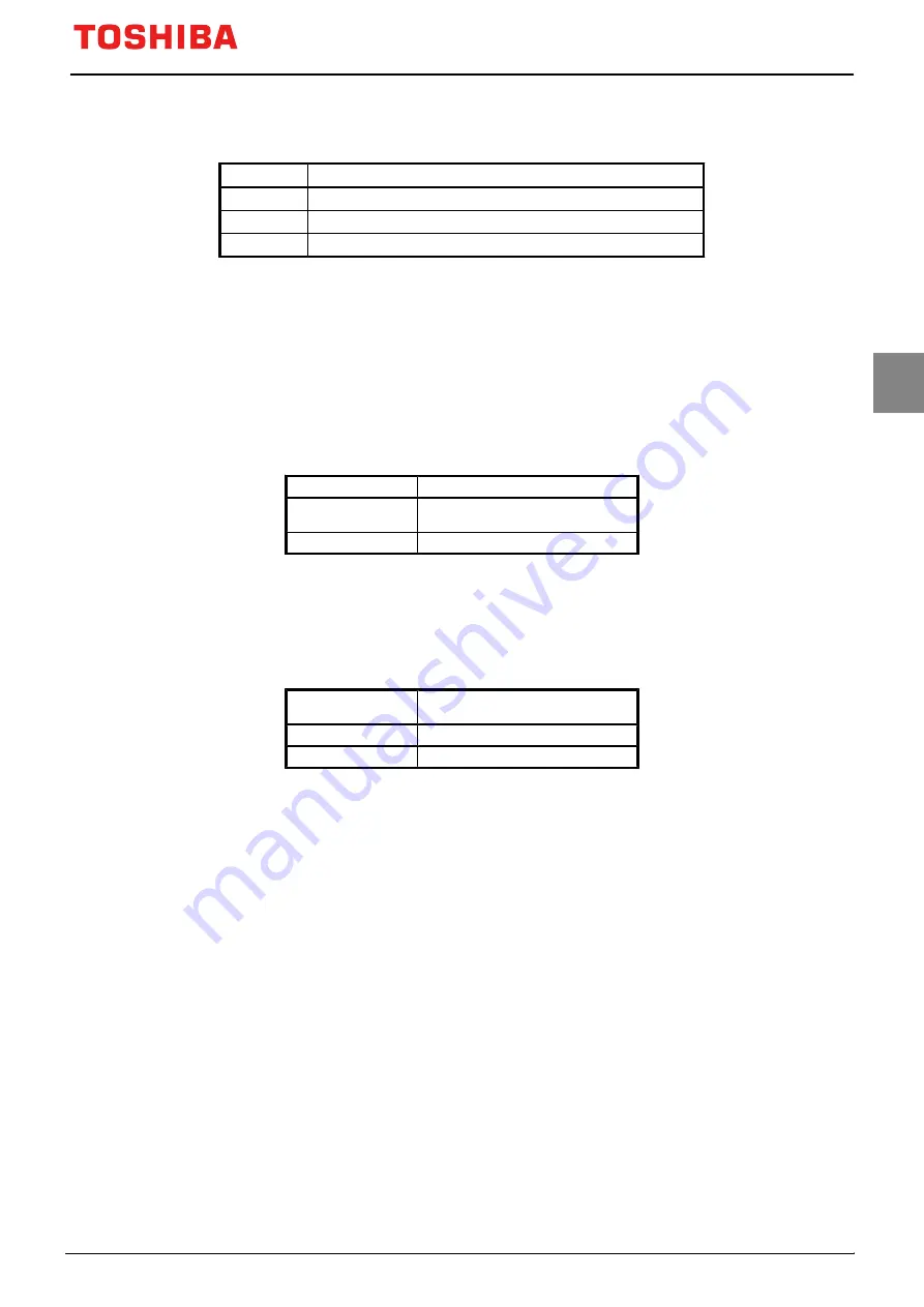
Table 22-16 ACK response to Flash memory chip erase and protect bit erase operation
Transmit data
Description
0x54
Determined as a erase enable command
0x4F
Erase command is complete.
0x4C
Erase command is abnormally terminated.
Note:
Even when an erase command is performed normally, a Negative acknowledge may be returned
by ACK response. Check the FCSR<RDY_BSY> to make sure the command sequence end, and
then hold for 200 μ s or more, after that reconfirm the erase status.
22.3.5.3 Password Determination
The boot program use the below area to determine whether a password is required or use as a password.
Area
Address
Password requirement
determination
0x3F81_FFF0 (1byte)
Password area
0x3F81_FFF4 to 0x3F81_FFFF (12byte)
The RAM Transfer command performs a password verification regardless of necessity judging data.
Flash memory chip erase or protect bit erase command performs a password verification only when neces-
sity judging is determined as "required".
Password requirement
setting
Data
Need password
Other than 0xFF
No password
0xFF
If a password is set to 0xFF (erased data), it is difficult to protect data securely due to an easy-to-guess
password. Even if Single Boot mode is not used, it is recommended to set a unique value as a password.
(1)
Password verification using RAM transfer command
If all these address locations contain the same bytes of data other than 0xFF, this condition is deter-
mined as a password area error as shown in Figure 22-11. In this case, the boot program returns an er-
ror acknowledge (0x11) in response to the 17th byte of checksum value regardless of the password ver-
ification.
The boot program verifies 5th byte to 16th byte of receive data (password data). A password er-
ror occurs if all 12 bytes do not match. If the password error is determined, an ACK response data
to the 17th of CHECK SUM data is a password error.
The password verification is performed even if the security function is enabled.
TMPM3V6/M3V4
Page 469
2019-02-06
Summary of Contents for TMPM3V4
Page 1: ...32 Bit RISC Microcontroller TX03 Series TMPM3V6 M3V4 ...
Page 2: ... 2019 Toshiba Electronic Devices Storage Corporation ...
Page 7: ...Revision History Date Revision Comment 2019 02 06 1 First Release ...
Page 8: ......
Page 22: ...xiv ...
Page 52: ...TMPM3V6 M3V4 3 Processor Core 3 6 Exclusive access Page 30 2019 02 06 ...
Page 148: ...TMPM3V6 M3V4 7 Exceptions 7 6 Exception Interrupt Related Registers Page 126 2019 02 06 ...
Page 178: ...TMPM3V6 M3V4 9 Input Output port 9 2 Block Diagrams of Ports Page 156 2019 02 06 ...
Page 354: ...TMPM3V6 M3V4 14 Synchronous Serial Port SSP 14 6 Frame Format Page 332 2019 02 06 ...
Page 419: ...TMPM3V6 M3V4 Page 397 2019 02 06 ...
Page 462: ...TMPM3V6 M3V4 21 Watchdog Timer WDT 21 5 Control register Page 440 2019 02 06 ...
Page 544: ......


