


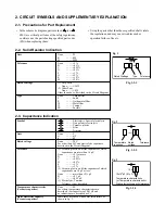


2-4. Inductor Indication
Unit
None
...........
Η
µ
...........
µ
H
m
........... mH
Tolerance
None
........... ±5%
B
........... ±0.1%
C
........... ±0.25%
D
........... ±0.5%
F
........... ±1%
G
........... ±2%
K
........... ±10%
M
........... ±20%
2-5. Waveform and Voltage Measurement
• The waveforms for CD/DVD and RF shown in the
circuit diagrams are obtained when a test disc is
played back.
• All voltage values except the waveforms are expressed
in DC and measured by a digital voltmeter.
Eg. 4
Eg. 5
Fig. 3-2-4
Fig. 3-2-5
Type name
10m
Type
Tolerance
Summary of Contents for SD-2050
Page 1: ...DVD VIDEO PLAYER SERVICE MANUAL May 2000 s FILE NO 810 200005 SD 2050 DIGITAL VIDEO ...
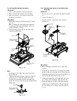
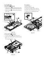
Page 5: ...SECTION 1 GENERAL DESCRIPTIONS SECTION 1 GENERAL DESCRIPTIONS 1 OPERATING INSTRUCTIONS ...
Page 51: ...47 Others Memo ...
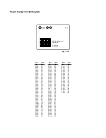
Page 80: ...4 2 Power Supply Block Diagram Fig 3 4 2 ...
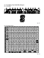
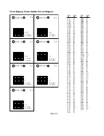
Page 82: ...Fig 3 4 5 4 3 3 Front Display Power Switch Block Diagram ...
Page 84: ...Fig 3 4 7 4 4 2 Logical System Block Diagram ...
Page 85: ...4 5 Output Block Diagram Fig 3 4 8 ...
Page 88: ...10 1 3 4 A B C D E G 2 5 6 7 8 9 F Fig 3 5 3 5 2 Front Display Power Switch Circuit Diagram ...
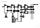
Page 95: ...Fig 3 5 5 5 3 2 Main Circuit Diagram ...
Page 96: ...5 3 2 Main Circuit Diagram ...
Page 97: ......
Page 98: ......
Page 99: ......
Page 100: ......
Page 101: ......
Page 102: ......
Page 103: ...Fig 3 5 5 ...
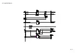
Page 105: ...Fig 3 5 6 10 1 3 4 A B C D E G 2 5 6 7 8 9 F 11 H 5 4 Output Circuit Diagram ...
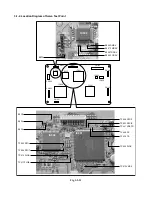
Page 115: ...10 1 3 4 A B C D E G 2 5 6 7 8 9 F Fig 3 6 6 EU01 Main PC Board Top pattern character symbol ...
Page 125: ......