


60
1-1-2. V Sync Separation Circuit
To separate a V sync signal from the composite sync signal
consisting of V and H sync signals mixed, two stages of
integration circuits are provided inside the IC. The circuit
consists of a differential circuit and a Miller integration
circuit, and has following functions.
(1) Removes H sync signal component.
(2) Maintain stable V sync performance for a tape recorded
with a copy guard.
(3) Stabilized V sync performance under special field
conditions (poor field, ghost, sync depressed, adjacent
channel best).
The V sync signal separated in this stage is processed in a
waveform shape circuit and then used as a reset pulse in the
V division circuit as stated later.
2. H AFC (Automatic Frequency Control)
CIRCUIT
A sync system which performs synchronization with each
waveform of the sync signal as performed in a sync system
in the V circuit is called a direct type sync system. However,
if the synchronization for the H oscillator is carried out with
this method, the H oscillator synchronizes with external
noises and the H synchronization will be disturbed. To
prevent this, an output of the H oscillator is compared with
a reference H sync signal to detect deviations of frequency
and phase. The H oscillator is automatically controlled with
the detected output averaged. This circuit is called an AFC
circuit.
In the N4SS chassis, a conventional AFC circuit is not
employed but a new double AFC circuit built-in the TA1222N
is used. Fig. 9-3 shows the AFC circuit and the block diagram
of the circuit.
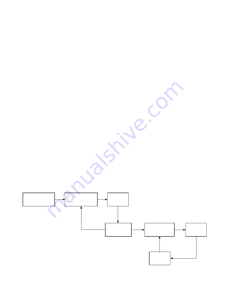
Fig. 9-3 H AFC circuit block diagram
First, phases of a 32 fH counted-down signal and a H sync
signal contained in broadcasting signal are compared in the
AFCI loop and the loop develops an H pulse signal for the
AFCII loop. That is, when a phase deference 01 exists in
comparison of the phase of fH signal developed by counting
down the 32 fH signal and the phase of H sync signal of the
broadcasting signal, an error signal corresponding to the
phase different is detected and a correction voltage ???1
corresponding to the error output is generated. With this
correction voltage, the 32 fH oscillator circuit is controlled.
The correction (control) voltage for the oscillator varies in
direction of positive or negative corresponding to phase lead
or lag of the fH pulse (developed by counting down) from the
H sync signal. As the H oscillator (32 x fH), a voltage
controlled oscillator (VCO), oscillation frequency and phase
of which can be controlled with the control voltage is used.
Next, an H pulse signal is created from the fH signal counted
down, and the pulse is used instead of the H sync signal in the
AFCII circuit. The AFCII circuit differs in the loop of the
count down circuit and H output circuit.
The AFCII circuit compares phase of a H BLK pulse created
by waveform shaping a AFC pulse from the FBT and a phase
of the H pulse, and detects an error component corresponding
to the phase difference 02 (if exist) and develops a
correction voltage V2 corresponding to the error, thereby
controlling the phase of Q501 H out.
The H output control voltage varies in a positive or negative
direction corresponding to the phase lead or lag of the H BLK
pulse from that of the H pulse. The phase of H out is varied
with the control voltage to make synchronization with the H
pulse phase.
The purpose of the double AFC circuit employed this time is
to improve horizontal jitter under signal reception in a poor
electrical field. The jitter in the poor field strength and
SYNC SEPARATION
CIRCUIT
PHASE DETECTION
CIRCUIT
32 x fH
VCO
H COUNT DOWN
(DIVIDING)
AFC I LOOP
PHASE DETECTION
CIRCUIT
AFC II LOOP
H DRIVE
H OUTPUT
CIRCUIT
FBT PULSE
(AFC PULSE)
Summary of Contents for CF35E50
Page 6: ...6 SECTION I OUTLINE ...
Page 13: ...13 7 CN32D90 BLOCK DIAGRAM ...
Page 16: ...16 SECTION II TUNER IF MTS S PRO MODULE ...
Page 24: ...24 SECTION III CHANNEL SELECTION CIRCUIT ...
Page 41: ...41 SECTION IV AUDIO OUTPUT CIRCUIT ...
Page 44: ...44 SECTION V A V SWITCHING CIRCUIT ...
Page 47: ...47 SECTION VI VIDEO PROCESSING CIRCUIT ...
Page 52: ...52 SECTION VII V C D IC ...
Page 55: ...55 SECTION VIII PIP MODULE ...
Page 58: ...58 SECTION IX SYNC SEPARATION H AFC H OSCILLATOR CIRCUITS ...
Page 63: ...63 SECTION X VERTICAL OUTPUT CIRCUIT ...
Page 69: ...69 SECTION XI HORIZONTAL DEFLECTION CIRCUIT ...
Page 85: ...85 SECTION XII DEFLECTION DISTORTION CORRECTION CIRCUIT Side DPC Circuit ...
Page 92: ...92 SECTION XIII CLOSED CAPTION EDS CIRCUIT ...
Page 98: ...98 SECTION XIV POWER CIRCUIT ...
Page 109: ...109 SECTION XV DSP CIRCUIT ...
Page 125: ...125 SECTION XVI FAILURE DIAGNOSIS PROCEDURES ...
Page 139: ......


