background image

THSB-FMC-01Vx1_UserManual_Rev1.0_E                                                                                                                                                                                   

Copyright©2017 THine Electronics, Inc.                                                                                                                            THine Electronics, Inc.

1


Security  E 

THSB-FMC-01V

X

1

User Manual

G

ENERAL 

D

ESCRIPTION

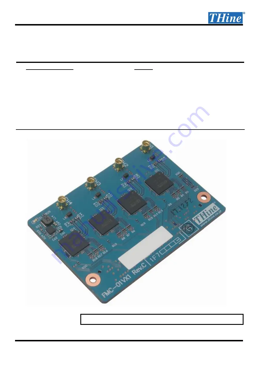
THSB-FMC-01Vx1 is an FMC/LPC daughter card 

supporting V-by-One

® 

HS receiver for the high-speed serial 

interface. Allows to receive four video streamings of 
V-by-One

® 

HS.

THCV236 is applied as V-by-One

® 

HS receiver to provide 

a stable communication system on long-distance cables.

THSB-FMC-01Vx1 also supports Power over Coax 

(PoC) system and enables to use V-by-One

® 

HS camera 

only with one coax cable.

F

EATURE

* W 70mm x H 50mm small size
* FMC/LPC Standard [Vita 57.1] Connector 
* Four MMCX connectors for V-by-One

® 

HS receiver

* V-by-One

® 

HS receiver THCV236, integrates adaptive

equalizer and stabilize communication system on
long-distance cable.

* Support POWER over COAX (PoC) using 5V
* Support 2.5 V or 3.3 V for VADJ power supply

F

OR SAFETY PURPOSES

,

SEE 

‘P

RECAUTIONS FOR 

P

O

C’

OF 

C

HAPTER 

3

Summary of Contents for THSB-FMC-01VX1

Page 1: ...e HSreceiver to provide a stable communication system on long distance cables THSB FMC 01Vx1alsosupportsPoweroverCoax PoC systemand enablestouseV by One HScamera onlywith onecoax cable FEATURE W70mmx H 50mmsmall size FMC LPC Standard Vita57 1 Connector Four MMCX connectors forV by One HS receiver V by One HSreceiverTHCV236 integratesadaptive equalizer andstabilize communicationsystemon long distan...

Page 2: ...ON 10 7 POWER SUPPLY SYSTEM 11 8 PIN ASSIGNMENT OF FMC CONNECTOR 11 9 PIN DESCRIPTION OF FMC CONNECTOR 14 10 POWER ON LED 15 FIGURE FIG 4 1 BLOCK DIAGRAM 8 FIG 5 1 TOP VIEW 9 FIG 5 2 BOTTOM VIEW 9 FIG 7 1 POWER SUPPLY SYSTEM 11 FIG 10 1 POWER ON LED 15 TABLE TABLE 8 1 COLOR INDICATOR FOR PIN ASSIGNMENT 11 TABLE 8 2 PIN ASSIGNMENT OF FMC C D COLUMNS 12 TABLE 8 3 PIN ASSIGNMENT OF FMC G H COLUMNS 13...

Page 3: ...conventions are used to indicate the possibility of injury damage and classify precautions if the product is handled incorrectly Danger Indicates the high possibility of serious injury or death if the product is handled incorrectly Warning Indicates the possibility of serious injury or death if the product is handled incorrectly Caution Indicates the possibility of injury or physical damage in con...

Page 4: ...n For inspection modification or repair contact our sales personnel Do not place the product on unstable locations Otherwise it may drop or fall resulting in injury to persons or failure If the product is dropped or damaged do not use it as is Otherwise a fire or electric shock may occur Do not touch the product with a metallic object Otherwise a fire or electric shock may occur Do not place the p...

Page 5: ...t or bookshelf Locations which receive oily smoke or steam Locations exposed to direct sunlight Locations close to heating equipment Closed inside of a car where the temperature becomes high Staticky locations Locations close to water or chemicals Otherwise a fire electric shock accident or deformation may occur due to a short circuit or heat generation Do not place heavy things on the product Oth...

Page 6: ...se of this product against the instructions given in this manual 4 Malfunctions due to connection to other devices THine Electronics Inc assumes no responsibility or liability for 1 Erasure or corruption of data arising from use of this product 2 Any consequences or other abnormalities arising from use of this product or 3 Damage of this product not due to our responsibility or failure due to modi...

Page 7: ...ct is applied POWER over COAX PoC system and output signals of MMCX are superimposed 5 V Power Supply Before using the product read this special precaution carefully Special Precaution Do not short output signals via MMCX connector to GND or other signals Otherwise the product may break down or it may cause a fire smoking or electric shock ...

Page 8: ...e HS FMC LPC Connector ASP 134604 01 VS HS DE Data 7 0 Clock MMCX 12V 5V 5V V by One HS VS HS DE Data 7 0 Clock MMCX 5V V by One HS VS HS DE Data 7 0 Clock MMCX 5V V by One HS VS HS DE Data 7 0 Clock MMCX 5V DC DC Switching Regulator V by One HS RX THCV236 V by One HS RX THCV236 V by One HS RX THCV236 V by One HS RX THCV236 SCL SDA PowerDown PowerDown PowerDown ...

Page 9: ...THSB FMC 01Vx1_UserManual_Rev1 0_E Copyright 2017 THine Electronics Inc THine Electronics Inc 9 Security E 5 Top Bottom View Fig 5 1 Top View Fig 5 2 Bottom View ...

Page 10: ...0 Security E 6 Board Specification Outline Size W 70mm x H 50mm Layer Structure 4 Layer Thickness of PCB 1 6 mm Material FR 4 FMC Connector Samtec ASP 134604 01 MMCX Connector Molex 0734151471 V by One HS Receiver THine Electronics THCV236 DC DC Switching Regulator Texas Instruments TLV62130RGTR ...

Page 11: ...X THCV236 4 2 5V 1A or 3 3V 1A 3P3VAUX MMCX 4 NC NC 7 Power Supply System Use 2 5 V or 3 3 V for VADJ voltage on your FPGA board Other voltage is not supported 8 Pin Assignment of FMC Connector Table 8 1 Color Indicator for Pin Assignment Color Indicator Description V by One HSchannel 1 V by One HSchannel 2 V by One HSchannel 3 V by One HSchannel 4 Use 2 5 V or 3 3 V for VADJ Power Supply on your ...

Page 12: ...1 LA06_N 11 LA05_P VBO1 DEI GND GND 12 LA05_N VBO1 HSI GND GND 13 GND GND NC LA10_P 14 LA09_P NC NC LA10_N 15 LA09_N NC GND GND 16 GND GND GND GND 17 LA13_P VBO2 D2 VBO2 CLK LA14_P 18 LA13_N VBO2 D3 NC LA14_N 19 GND GND GND GND 20 LA17_P_CC VBO3 CLK GND GND 21 LA17_N_CC NC NC LA18_P_CC 22 GND GND NC LA18_N_CC 23 LA23_P NC GND GND 24 LA23_N NC GND GND 25 GND GND NC LA27_P 26 LA26_P NC VBO SCL LA27_...

Page 13: ..._N 13 LA07_P NC GND GND 14 LA07_N VBO2 D0 VBO2 D1 LA12_P 15 GND GND VBO2 HSI LA12_N 16 LA11_P VBO2 DEI GND GND 17 LA11_N VBO2 VSI VBO2 D4 LA16_P 18 GND GND VBO2 D6 LA16_N 19 LA15_P VBO2 D5 GND GND 20 LA15_N VBO2 D7 VBO3 D0 LA20_P 21 GND GND VBO3 DEI LA20_N 22 LA19_P VBO3 D1 GND GND 23 LA19_N VBO3 HSI VBO3 VSI LA22_P 24 GND GND VBO3 D3 LA22_N 25 LA21_P VBO3 D2 GND GND 26 LA21_N VBO3 D4 VBO3 D5 LA25...

Page 14: ...2 Horizontal SYNC VBO2 DEI LA11_P Output THCV236 channel2 Data Enable VBO2 D0 LA07_N Output THCV236 channel2 pixel data bit 0 VBO2 D1 LA12_P Output THCV236 channel2 pixel data bit 1 VBO2 D2 LA13_P Output THCV236 channel2 pixel data bit 2 VBO2 D3 LA13_N Output THCV236 channel2 pixel data bit 3 VBO2 D4 LA16_P Output THCV236 channel2 pixel data bit 4 VBO2 D5 LA15_P Output THCV236 channel2 pixel data ...

Page 15: ...nnel4 pixel data bit 2 VBO4 D3 LA30_N Output THCV236 channel4 pixel data bit 3 VBO4 D4 LA33_P Output THCV236 channel4 pixel data bit 4 VBO4 D5 LA32_P Output THCV236 channel4 pixel data bit 5 VBO4 D6 LA33_N Output THCV236 channel4 pixel data bit 6 VBO4 D7 LA32_N Output THCV236 channel4 pixel data bit 7 VBO4 PDN CLK1_M2C_N Input THCV236 channel4 Power Down Active High VBO SCL LA27_N Input I2C serial...

Page 16: ...erial without our prior permission is prohibited 3 Note that if infringement of any third party s industrial ownership should occur by using this product we will be exempted from the responsibility unless it directly relates to the production process or functions of the product 4 Please note that this product is not designed to be radiation proof 5 Customers are asked if required to judge by thems...

Reviews: