Texas Instruments UCC25640EVM-020 User Manual Download Page 19

www.ti.com

Performance Data and Typical Characteristic Curves

19

SLUUBX3B – June 2019 – Revised November 2019

Submit Documentation Feedback

Copyright © 2019, Texas Instruments Incorporated

UCC25640EVM-020 Evaluation Module
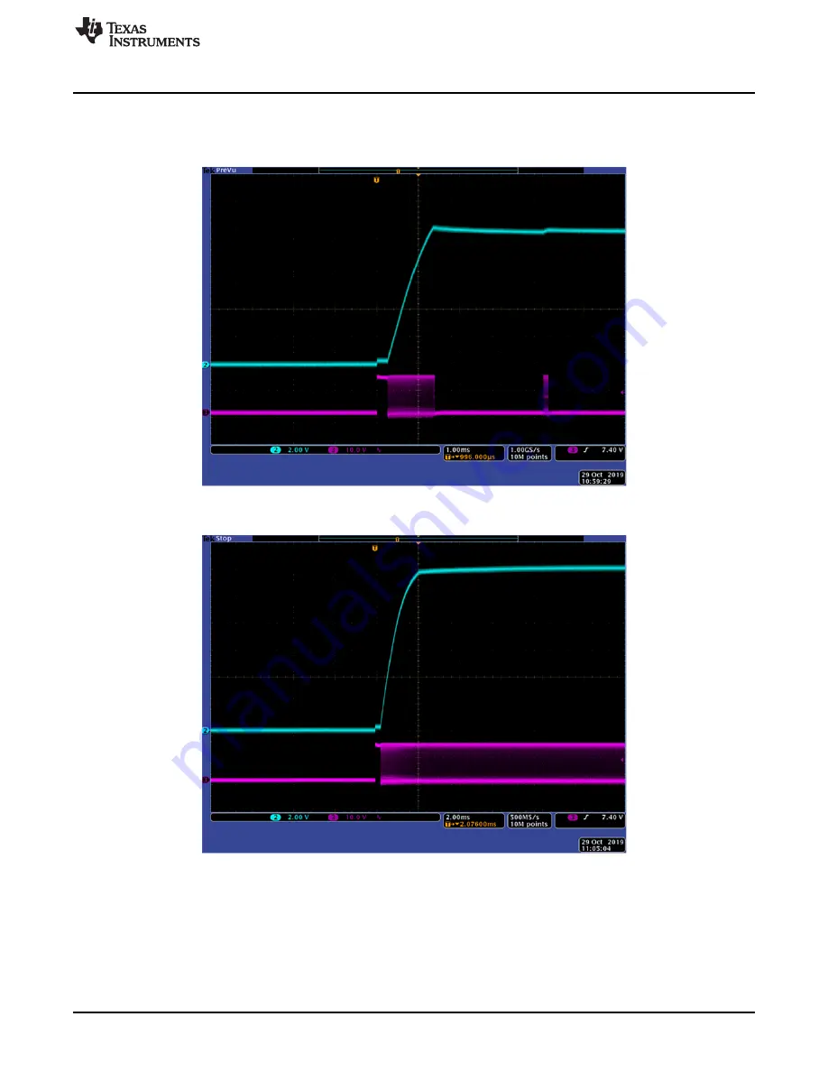
9.7

Startup

The following waveforms show the output voltage and low side gate behavior. 115 VAC, 60 Hz is applied
initially to the AC input, then the 390 VDC input is applied to the DC input

Figure 13. No Load (0 A) Startup (Ch2 = V

OUT

; Ch3 = LO)

Figure 14. Full Load (15 A) Startup (Ch2 = V

OUT

; Ch3 = LO)

Summary of Contents for UCC25640EVM-020

Page 1: ...UCC25640EVM 020 Evaluation Module User s Guide Literature Number SLUUBX3B June 2019 Revised November 2019 ...

Page 2: ...rom further use of the HV EVM 1 Work Area Safety a Keep work area clean and orderly b Qualified observer s must be present anytime circuits are energized c Effective barriers and signage must be present in the area where the TI HV EVM and its interface electronics are energized indicating operation of accessible high voltages may be present for the purpose of protecting inadvertent access d All in...

Page 3: ...M or its electrical circuits as they could be at high voltages capable of causing electrical shock hazard 3 Personal Safety a Wear personal protective equipment e g latex gloves or safety glasses with side shields or protect EVM in an adequate lucent plastic box with interlocks from accidental touch Limitation for safe use EVMs are not to be used as all or part of a production unit ...

Page 4: ...tand alone LLC resonant half bridge DC DC power converter designed to operate with DC input from 365 VDC to 410 VDC AC input from 85 to 265 VRMS 47 to 63 Hz and a nominal output of 12 VDC up to 180 W The EVM is delivered using a diode rectifier at the output The user has the option to evaluate this converter with a synchronous rectifier SR by populating the UCC24624 and SR FETs This user s guide p...

Page 5: ... Full load power of 180 W or full load current of 15 A High efficiency Optimized low power features enable extremely low standby power Advanced burst mode with burst soft on and soft off for minimized audible noise Adaptive dead time X capacitor discharge Over temperature output over voltage and three level over current protections Test points to facilitate device and topology evaluation 2 3 Using...

Page 6: ...is delivered using the diode rectifier at the output The option to evaluate the converter with synchronous rectification SR is available to the user SR is often used to increase efficiency by replacing the freewheeling diode with a lower loss FET To use this EVM with UCC24624 Remove D2 and D5 Populate R31 and R32 with 0Ω Populate R35 with 10Ω Populate R53 and R54 with 532Ω Populate R55 with 39 2Ω ...

Page 7: ...ge frequency 47 63 Hz Input DC UVLO On 365 VDC Input DC UVLO Off 330 VDC OUTPUT CHARACTERISTICS VOUT Output voltage Normal mode Burst mode threshold to full load 15 A 12 VDC VOUT Output voltage Standby mode No load to burst mode threshold 9 75 VDC Burst mode threshold output current limit rising 240 mA Burst mode threshold output current limit falling 110 mA IOUT Output load current 365 to 410 VDC...

Page 8: ...i com 8 SLUUBX3B June 2019 Revised November 2019 Submit Documentation Feedback Copyright 2019 Texas Instruments Incorporated UCC25640EVM 020 Evaluation Module 4 Schematic Diagram Figure 3 UCC25640EVM 020 Power Stage Schematic ...

Page 9: ...Schematic Diagram 9 SLUUBX3B June 2019 Revised November 2019 Submit Documentation Feedback Copyright 2019 Texas Instruments Incorporated UCC25640EVM 020 Evaluation Module Figure 4 UCC25640EVM 020 Control Schematic ...

Page 10: ...0 W and current limit function The AC voltage source to be used should meet IEC 60950 reinforced insulation requirement DC Digital Multimeter One unit capable of 0 VDC to 450 VDC input range four digit display preferred and one unit capable of 0 VDC to 20 VDC input range four digit display preferred Output Load DC load capable of receiving 0 VDC to 20 VDC 0 A to 15 A and 0 W to 300 W or greater wi...

Page 11: ...nstruments Incorporated UCC25640EVM 020 Evaluation Module 5 2 Recommended Test Setup Figure 5 UCC25640EVM 020 Test Setup Diagram WARNING High voltages that may cause injury exist on this evaluation module EVM Please ensure all safety procedures are followed when working on this EVM Never leave a powered EVM unattended ...

Page 12: ...c describe how to connect the UCC28056EVM 296 or UCC28064EVM 004 Transition Mode TM PFC Controllers to this EVM 1 Remove D8 and D9 from UCC25640EVM 020 2 Connect the anode of D8 to AC Line and the anode of D9 to AC Neutral on UCC28056EVM 296 or UCC28064EVM 004 3 Connect both the cathodes of D8 and D9 to TP14 on UCC25640EVM 020 4 Connect TP15 RVCC on UCC25640EVM 020 to TP9 VCC on UCC28056EVM 296 or...

Page 13: ...GND Primary side ground TP10 VOUT Output voltage positive terminal TP11 INJECT Small signal injection terminal TP12 FB_Current Feedback current measurement TP13 HV High voltage start pin TP14 AC_Rect Rectified AC input TP15 RVCC Regulated 12 V supply TP16 BLK Input voltage sensing TP17 AC_L AC line TP18 AC_N AC neutral TP19 LL SS Soft start and light load burst mode threshold TP20 ISNS Resonant cu...

Page 14: ...sure circuit protection 4 Keep the AC voltage source output off Connect the source with AC_neutral to J8 1 AC_earth to J8 2 and AC_line to J8 3 Isolate the AC voltage source and meet the IEC 60950 requirement Set the AC output voltage and frequency within the range specified in Table 1 between 85 and 265 VAC and 47 to 63 Hz Set the AC source current limit to 200 mA 5 Connect an electronic load set...

Page 15: ... 20 9 739 194 772 389 820 0 672 261 815 50 9 739 486 925 389 814 1 514 590 186 100 9 738 973 820 389 807 2 914 1135 799 9 2 PFC Boost Front End Standby Power 9 2 1 Overview UCC256404 includes a high voltage startup feature This feature enables the controller to be powered by a wide AC input eliminating the need for an external supply to power both the PFC and LLC When AC power is applied to UCC256...

Page 16: ...T A POUT W Efficiency 90 0 218 9 697 0 0124 0 120 54 94 115 0 216 9 697 0 0124 0 120 55 44 230 0 223 9 697 0 0124 0 120 53 70 265 0 227 9 697 0 0124 0 120 52 76 90 0 361 9 697 0 0248 0 240 66 56 115 0 360 9 696 0 0248 0 240 66 74 230 0 364 9 697 0 0248 0 240 66 01 265 0 365 9 697 0 0248 0 240 65 83 Table 6 Total Standby Power with UCC28064EVM 004 PFC and UCC25640EVM 020 LLC VIN V PIN W VOUT V IOUT...

Page 17: ...19 Texas Instruments Incorporated UCC25640EVM 020 Evaluation Module 9 4 Load Regulation Figure 9 illustrates the load regulation versus output current graph Figure 9 Load Regulation vs Output Current 9 5 Switching Frequency Figure 10 illustrates the converter switching frequency versus output current Figure 10 Switching Frequency vs Output Current ...

Page 18: ...ts Incorporated UCC25640EVM 020 Evaluation Module 9 6 Audible Noise Figure 11 and Figure 12 show the audible noise measurements during light load standby operation The measurements are performed in a soundproof container with the microphone 5 mm above the transformer Figure 11 Audible Noise Measurement at 10 mA Load Figure 12 Audible Noise Measurement at 20 mA Load ...

Page 19: ...19 Texas Instruments Incorporated UCC25640EVM 020 Evaluation Module 9 7 Startup The following waveforms show the output voltage and low side gate behavior 115 VAC 60 Hz is applied initially to the AC input then the 390 VDC input is applied to the DC input Figure 13 No Load 0 A Startup Ch2 VOUT Ch3 LO Figure 14 Full Load 15 A Startup Ch2 VOUT Ch3 LO ...

Page 20: ...Module 9 8 Thermal Image The following images show the EVM temperature after 20min soak at full load no forced air and 390Vdc input applied to the DC input Figure 15 Thermal Image Top Table 7 Component Temperature Component Temperature C T1 Bx1 74 9 C D2 Bx2 90 2 C Figure 16 Thermal Image Bottom Table 8 Component Temperature Component Temperature C U4 Bx1 42 3 C Q1 Bx2 44 9 C Q3 Bx3 46 1 C R9 R12 ...

Page 21: ...exas Instruments Incorporated UCC25640EVM 020 Evaluation Module 9 9 Output Voltage Ripple The following waveforms show the output voltage ripple with 115 VAC 60 Hz applied to the AC input and 390 VDC applied to the DC input The oscilloscope probe is AC coupled Figure 17 No Load 0 A Output Ripple Ch2 VOUT Figure 18 Full Load 15 A Output Ripple Ch2 VOUT ...

Page 22: ...ed to the AC input and 390 VDC applied to the DC input Figure 20 illustrates the dynamic voltage scaling through the entry and exit of burst mode The output voltage immediately exits standby mode increasing to 12 V when the BMT is exceeded It then drops to the 9 75 V standby output voltage level when the load falls below the BMT This behavior is due to the circuit explained in Section 10 2 Figure ...

Page 23: ... Submit Documentation Feedback Copyright 2019 Texas Instruments Incorporated UCC25640EVM 020 Evaluation Module 9 11 Loop Response The following plot shows the loop response with 115 VAC 60 Hz applied to the AC input and 390 VDC applied to the DC input at full load condition Figure 21 Bode Plot at 15 A Load ...

Page 24: ...12 Steady State The following waveforms show the sampled resonant capacitor voltage VCR resonant current and low side gate voltage LO with 115 VAC 60 Hz applied to the AC input and 390 VDC applied to the DC input Figure 22 and Table 7 show the waveforms during burst mode Figure 22 Steady State Waveforms at No Load Ch2 VCR Ch3 LO Ch4 IResonant Figure 23 Steady State Waveforms at 15 A Load Ch2 VCR C...

Page 25: ...ht 2019 Texas Instruments Incorporated UCC25640EVM 020 Evaluation Module 9 13 X Capacitor Discharge The following waveform shows the X Capacitor discharge after the AC input is disconnected at the peak of a 265 VAC input 390 VDC is applied to the DC input and the output is unloaded Figure 24 X Cap Discharge Ch1 Voltage across X Cap C40 and C41 ...

Page 26: ...bmit Documentation Feedback Copyright 2019 Texas Instruments Incorporated UCC25640EVM 020 Evaluation Module 10 Assembly Drawing and List of Materials 10 1 Assembly Drawing Figure 25 UCC25640EVM 020 Top Layer Assembly Drawing Top view Figure 26 UCC25640EVM 020 Bottom Layer Assembly Drawing Top view ...

Page 27: ...e 2019 Revised November 2019 Submit Documentation Feedback Copyright 2019 Texas Instruments Incorporated UCC25640EVM 020 Evaluation Module Figure 27 UCC25640EVM 020 Top Copper Assembly Drawing Top view Figure 28 UCC25640EVM 020 Bottom Copper Assembly Drawing Top view ...

Page 28: ...de the output voltage is reduced and the LLC converter is configured to operate in burst mode to minimize input power A central control circuit communicates with the AC DC power supply to enter or exit standby mode as needed In order to mimic this system level behavior an external standby circuit was added to this design This external standby circuit adjusts both the burst mode threshold setting a...

Page 29: ...s compared to a set reference voltage to determine when to enter or exit standby mode Hysteresis is implemented on the comparator using R52 and R48 Figure 30 External Standby Circuit Current Sense Gain and Comparator The standby circuit adjusts the output voltage set point by changing the feedback resistor divider ratio through Q6 and R56 When in standby mode the gate of Q6 is held low When out of...

Page 30: ...st threshold 0 2V For applications where the output voltage set point is decreased when in standby mode it is possible to get in and out of burst mode by changing the output voltage regulation set point This is because the change in necessary peak to peak voltage on the VCR waveform to regulate at the higher output voltage is greater than the programmed burst threshold For these applications the b...

Page 31: ... C27 C28 2 Capacitor ceramic 1 uF 16 V 10 X7R 0603 EMK107B7105KA T C29 1 Capacitor ceramic 2 2 uF 16 V 10 X7R 1206 C1206C225K4RACTU C30 C31 2 Capacitor ceramic 4 7 uF 25 V 10 X7R 1206 C3216X7R1E475K085AB C32 C33 2 Capacitor ceramic 10 pF 16 V 10 C0G 0402 C0402C100K4GACTU C36 1 Capacitor ceramic 0 068 µF 25 V 10 X7R 0603 885012206070 C37 C45 2 Capacitor ceramic 0 1 uF 16 V 10 X5R 0402 GRM155R61C104...

Page 32: ...2064M99FKEA R36 1 Resistor 549k 1 0 125 W AEC Q200 Grade 0 0805 ERJ 6ENF5493V R37 1 Resistor 41 2 k 1 0 1 W 0603 RC0603FR 0741K2L R38 1 Resistor 316k 1 0 1 W 0603 RC0603FR 07316KL R39 R40 R45 R49 4 Resistor 10 M 5 0 25 W AEC Q200 Grade 0 1206 CRCW120610M0JNEA R41 R42 2 Resistor 4 75 1 0 063 W AEC Q200 Grade 0 0402 CRCW04024R75FKED R43 R47 3 Resistor 10 0 k 1 0 1 W 0603 RC0603FR 0710KL R44 1 Resist...

Page 33: ...ion Changes from A Revision August 2019 to B Revision Page Added component list to support UCC256402 5 Changed component list to support UCC256403 5 Changed component list to support UCC24624 6 Changed schematic diagram 8 Changed Efficiency vs Output Current graph 16 Changed Load Regulation vs Output Current graph 17 Changed Switching Frequency vs Output Current graph 17 Changed No load startup an...

Page 34: ...other than TI b the nonconformity resulted from User s design specifications or instructions for such EVMs or improper system design or c User has not paid on time Testing and other quality control techniques are used to the extent TI deems necessary TI does not test all parameters of each EVM User s claims against TI under this Section 2 are void if User fails to notify TI of any apparent defects...

Page 35: ... These limits are designed to provide reasonable protection against harmful interference in a residential installation This equipment generates uses and can radiate radio frequency energy and if not installed and used in accordance with the instructions may cause harmful interference to radio communications However there is no guarantee that interference will not occur in a particular installation...

Page 36: ...y for convenience and should be verified by User 1 Use EVMs in a shielded room or any other test facility as defined in the notification 173 issued by Ministry of Internal Affairs and Communications on March 28 2006 based on Sub section 1 1 of Article 6 of the Ministry s Rule for Enforcement of Radio Law of Japan 2 Use EVMs only after User obtains the license of Test Radio Station as provided in R...

Page 37: ... any interfaces electronic and or mechanical between the EVM and any human body are designed with suitable isolation and means to safely limit accessible leakage currents to minimize the risk of electrical shock hazard User assumes all responsibility and liability for any improper or unsafe handling or use of the EVM by User or its employees affiliates contractors or designees 4 4 User assumes all...

Page 38: ...OR DAMAGES ARE CLAIMED THE EXISTENCE OF MORE THAN ONE CLAIM SHALL NOT ENLARGE OR EXTEND THIS LIMIT 9 Return Policy Except as otherwise provided TI does not offer any refunds returns or exchanges Furthermore no return of EVM s will be accepted if the package has been opened and no return of the EVM s will be accepted if they are damaged or otherwise not in a resalable condition If User feels it has...

Page 39: ...se resources are subject to change without notice TI grants you permission to use these resources only for development of an application that uses the TI products described in the resource Other reproduction and display of these resources is prohibited No license is granted to any other TI intellectual property right or to any third party intellectual property right TI disclaims responsibility for...

Page 40: ...Mouser Electronics Authorized Distributor Click to View Pricing Inventory Delivery Lifecycle Information Texas Instruments UCC25640EVM 020 ...

Reviews: