www.ti.com
4
Reference
4.1
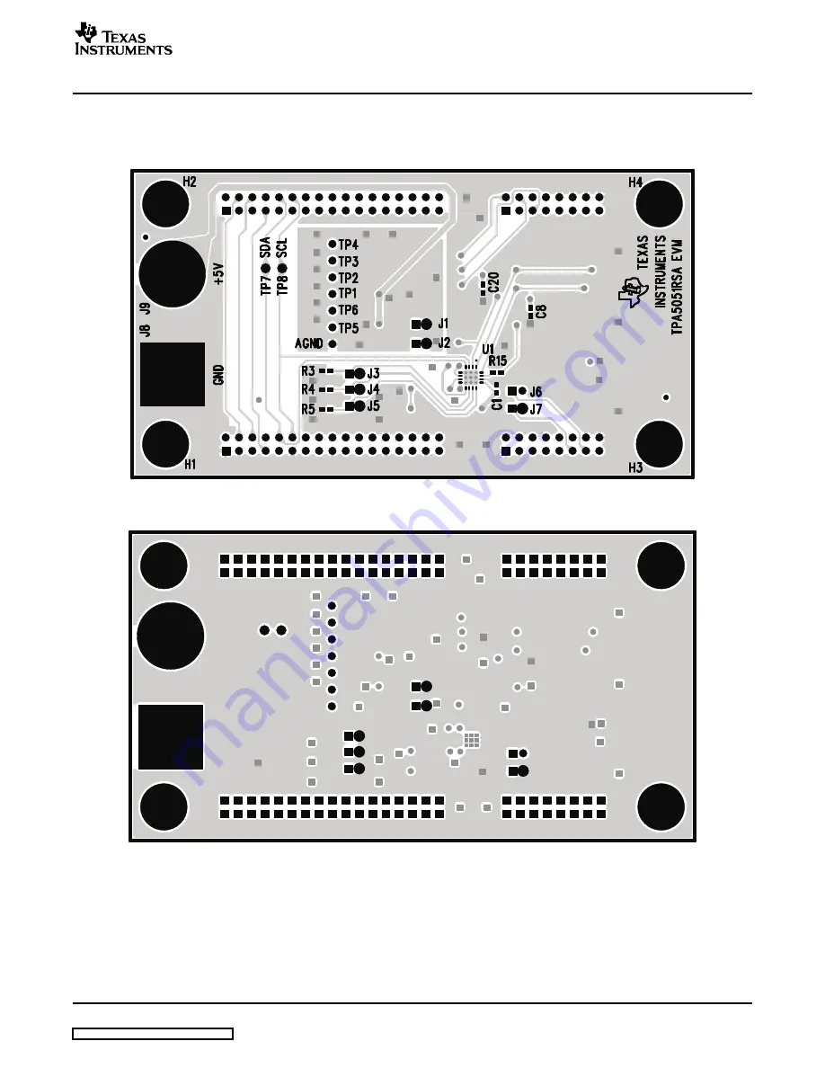
TPA5051EVM PCB Layers
Figure 7. TPA5051EVM Top Layer
Figure 8. TPA5051EVM Second Layer
SLOU184 – July 2006
TPA5051EVM
9
Submit Documentation Feedback
Page 1: ...er external components mounted on a printed circuit board PCB that can be used to independently delay two digital audio streams Each digital audio stream consists of a left and right channel both of w...
Page 2: ...l License Agreement must be read and accepted for installation to continue 9 On acceptance of the Command Tool License Agreement Net Framework 1 1 is installed This installation procedure may take a w...
Page 3: ...roblem are to depress and release the reset button on the TI Input USB board check to see that all cables are properly connected restart the TPA5051 GUI remove and then re insert the USB cable into th...
Page 4: ...www ti com Software Figure 2 TPA5051 in I2 S Mode With Frame Delay 4 TPA5051EVM SLOU184 July 2006 Submit Documentation Feedback...
Page 5: ...www ti com Software Figure 3 TPA5051 in Right Justified Mode SLOU184 July 2006 TPA5051EVM 5 Submit Documentation Feedback...
Page 6: ...ure that all external power sources are set to OFF 2 Connect an external regulated power supply set to 5 V to the module 5V J7 and GND J6 taking care to observe marked polarity 1 Ensure that the shunt...
Page 7: ...ay another TPA5051EVM can be added in series using the 16 pin and 34 pin ribbon cables 7 Install shunts across J6 and J7 For stand alone evaluation the shunts may be removed allowing for separate LRCL...
Page 8: ...board is designed to output I2 S only 9 Use scope probes to view both delayed and nondelayed signals via the DAC TP1 and TP2 left and right respectively are the delayed signals from DATA_OUT1 of the...
Page 9: ...www ti com 4 Reference 4 1 TPA5051EVM PCB Layers Reference Figure 7 TPA5051EVM Top Layer Figure 8 TPA5051EVM Second Layer SLOU184 July 2006 TPA5051EVM 9 Submit Documentation Feedback...
Page 10: ...www ti com Reference Figure 9 TPA5051EVM Third Layer Figure 10 TPA5051EVM Bottom Layer TPA5051EVM 10 SLOU184 July 2006 Submit Documentation Feedback...
Page 11: ...emet C19 T494A106M016AS L1 1 600 Ferrite 600 Ferrite Bead 0805 500mA 200 m 445 1554 2 ND TDK Bead DCR MMZ2012R601A L2 1 0 Jumper 0 Jumper 1 8W 0805 Ceramic P0 0ACT ND Panasonic ERJ 6GEY0R00V H1 H2 2 3...
Page 12: ...Materials continued Part No QTY Value Description Distributor No 1 Manufacturer Part No U5 1 EXB 8 Resistor array 39 5 1 16W Y1390TR ND Panasonic 2HV390JV EXB 2HV390JV The TPA5051EVM schematic diagram...
Page 13: ...Tpa5051evm6noB sch 1 Thu Jun 01 19 05 22 2006...
Page 14: ...r to handling the product This notice contains important safety information about temperatures and voltages For additional information on TI s environmental and or safety programs please contact the T...
Page 15: ...iness practice TI is not responsible or liable for any such statements TI products are not authorized for use in safety critical applications such as life support where a failure of the TI product wou...