background image

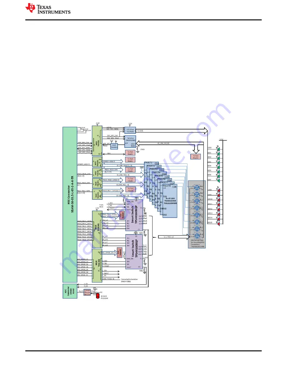
3.3.2 IO-Link Section Overview and Major Component Description

The IO-Link section of this board implements an IO-Link master using the TIOL111 device PHY and surrounding 
components needed to build a complete IO-Link master design. Therefore, on the physical side in addition to the 
TIOL111 device, a power supply for the ports, as well as a current sink is necessary. Also the hardware must be 
able to drive the wake-up pulse.

On the other side it is necessary to have a hardware as well as frame handler that support all three 
communication speeds. The TIOL111 device used as PHY here can handle all speeds (COM1, COM2, COM3). 
The eight port frame handler is implemented on the PRU of the used AM64x.

To realize an eight-port master, this design consists of eight M12 connectors and eight 

TIOL111DMWR 

IO-Link 

PHYs and associated LEDs. The IO-Link circuit is supported by two 

TPS4H160BQPWPRQ1 

Quad channel 

smart high-side switches for the L+ signals and a 

SN65HVS882 

serializer to support the D signals. The D 

signals are connected to a 10 pin header J21 for testing purpose. Both parts require a +24V which is supplied 
by a power jack on the board. A 

TLC59282 

16bit IO expander is also included to drive the 16 LEDs. The 

SN65HVS882 and 

TLC59282 

16bit IO expander are controlled by 

SOC_SPI1 

interface from GP EVM Board. 

SOC_SPI0. SOC_SPI1_CS0 is connected to the serializer and SOC_SPI1_CS1 is connected to the LED driver.

Figure 3-4. IO-Link Section Functional Block Diagram

www.ti.com

System Description

SPRUJ06 – OCTOBER 2021

Submit Document Feedback

TMDS64DC01EVM and TMDS243DC01EVM User's Guide

7

Copyright © 2021 Texas Instruments Incorporated

Summary of Contents for TMDS243DC01EVM

Page 1: ... Diagram 7 Figure 3 5 Power Input 11 List of Tables Table 1 1 TMDS64DC01EVM and TMDS243DC01EVM Feature Comparison 2 Table 2 1 TMDS64DC01EVM and TMDS243DC01EVM PCB Design Revisions and Assembly Variants 3 Table 3 1 TMDS64DC01EVM and TMDS243DC01EVM Key Features 4 Table 3 2 Functionality Selected by J11 Header 6 Table 3 3 HSE Connector Signal Routing 9 Table 3 4 150 Pin HSE Connector SEAM 30 03 5 L 0...

Page 2: ...e configuration and diagnostics An unshielded three wire cable as long as 20 meters normally equipped with M12 connectors establishes an IO Link connection Data rates range up to 230 kbps with a nonsynchronous minimum cycle time of 400 μs 10 Four operating modes support bidirectional input output I O digital input digital output and deactivation Security mechanisms and deterministic data delivery ...

Page 3: ...plements only the breakout section of the board PROC102A 0011 First production release of the AM64x EVM IO Link and High Speed Expansion Board Implements both the breakout and IO Link sections of the board PROC102A 002 First production release of the AM243x EVM High Speed Expansion Board Implements only the breakout section of the board 1 The TMDS64D01EVM E1 boards do not have a sticker indicating...

Page 4: ...M s HSE connector on standard 0 1 header pins Yes Yes Signal routing of HSE connector signals between Test Headers and IO Link section via user configurable FET switches Yes Yes Large prototyping area with 0 1 pitch holes Yes Yes Precision current monitoring with onboard INA253 Yes No not populated System Description www ti com 4 TMDS64DC01EVM and TMDS243DC01EVM User s Guide SPRUJ06 OCTOBER 2021 S...

Page 5: ...block diagram of the IO Link Breakout Board Figure 3 2 TMDS64DC01EVM Functional Block Diagram www ti com System Description SPRUJ06 OCTOBER 2021 Submit Document Feedback TMDS64DC01EVM and TMDS243DC01EVM User s Guide 5 Copyright 2021 Texas Instruments Incorporated ...

Page 6: ...FET switches are controlled using the J11 Header Connecting the control signal of all the MUXes to ground routes all signals from the HSE connector to the Breakout board whereas connecting the control signal to VCC3V3_IO_HSE routes all signals from the Mux to the IO Link section Table 3 2 Functionality Selected by J11 Header J11 Header Selection Functionality Supported Board Short J11 pins 1 and 2...

Page 7: ...port master this design consists of eight M12 connectors and eight TIOL111DMWR IO Link PHYs and associated LEDs The IO Link circuit is supported by two TPS4H160BQPWPRQ1 Quad channel smart high side switches for the L signals and a SN65HVS882 serializer to support the D signals The D signals are connected to a 10 pin header J21 for testing purpose Both parts require a 24V which is supplied by a pow...

Page 8: ...LIM Thus changing the current limit requires the change of RLIM to a different value via RLIM n VREF I LIM While the device is specified for a current limit of 3 6 mA via RLIM 25 kΩ The DI signals from the M12 connectors are connected to the input channels of the serializer The serializer is SPI compatible Upon a low level at the load input LD the information of the field inputs IP0 to IP7 is latc...

Page 9: ...PO6_HDR J4 PRG0_PRU1GPO8 EN_PHY_2 PRG0_PRU1GPO8_HDR PRG0_PRU1GPO11 EN_PHY_3 PRG0_PRU1GPO11_HDR J5 PRG0_PRU1GPO12 EN_PHY_4 PRG0_PRU1GPO12_HDR PRG0_PRU1GPO13 EN_PHY_5 PRG0_PRU1GPO13_HDR PRG0_PRU1GPO14 EN_PHY_6 PRG0_PRU1GPO14_HDR PRG0_PRU1GPO15 EN_PHY_7 PRG0_PRU1GPO15_HDR PRG0_PRU1GPO16 EN_PHY_8 PRG0_PRU1GPO16_HDR PRG0_PRU1GPO2 U7 EN_L 5 PRG0_PRU1GPO2_HDR J4 PRG0_PRU0GPO18 EN_L 1 PRG0_PRU0GPO18_HDR P...

Page 10: ...I_HDR SOC_SPI1_CLK SOC_SPI1_CLK_SE LED SOC_SPI1_CLK_HDR SOC_SPI1_CS0 SOC_SPI1_CS0_SE SOC_SPI1_CS0_HDR SOC_SPI1_CS1 LATCH SOC_SPI1_CS1_HDR HSE_MCAN1_RX I2C3_SDA HSE_MCAN1_RX I2C3_SDA J3 HSE_MCAN1_TX I2C3_SCL HSE_MCAN1_TX I2C3_SCL HSE_MCAN0_TX UART4_RXD HSE_MCAN0_TX UART4_RXD HSE_MCAN0_RX UART4_TXD HSE_MCAN0_RX UART4_TXD GPMC0_ADC 8 9 GPMC0_ADC 8 9 J6 GPMC0_ADC 10 15 GPMC0_ADC 10 15 J7 GPMC0_CSN2 GP...

Page 11: ... by example UL CSA VDE CCC PSE and so forth 3 3 4 Board Mating Connections The pinout for the mating connectors of the IO Link Breakout Board are listed in Table 3 4 Note The following HSE Connector pin names do not indicate exhaustive SoC Pin functionality For a full list of pin and signal functions see the device specific GP EVM User s Guide and data sheet Table 3 4 150 Pin HSE Connector SEAM 30...

Page 12: ..._GPIO0_35 A25 DGND B25 DGND A26 B26 DGND A27 VCC3V3_IO_HSE B27 DGND A28 VCC3V3_IO_HSE B28 DGND A29 VCC3V3_IO_HSE B29 HSE_PRG0_PRU0_GPO10 A30 B30 DGND C1 SOC_SPI1_CLK D1 SOC_SPI1_CS0 C2 VCC1V8_HSE D2 SOC_SPI1_CS1 C3 VCC1V8_HSE D3 MCU_RESETZ C4 DGND D4 DGND C5 PRG0_PRU0GPO13 D5 PRG0_PRU1GPO13 C6 PRG0_PRU0GPO5 D6 PRG0_PRU1GPO5 C7 DGND D7 DGND C8 PRG0_PRU1GPO3 D8 PRG0_PRU0GPO6 C9 PRG0_PRU0GPO14 D9 PRG...

Page 13: ...C0_DIR E4 HSE_DETECT E19 GPMC0_CSN1 E5 DGND E20 DGND E6 DGND E21 GPMC0_AD11 E7 DGND E22 DGND E8 PRG0_PRU0GPO1 E23 HSE_PRG0_PRU1_GPO9 E9 PRG0_PRU0GPO16 E24 HSE_MCAN0_RX UART4_TXD E10 DGND E25 DGND E11 PRG0_PRU1GPO6 E26 HSE_GPIO0_38 E12 PRG0_PRU1GPO14 E27 HSE_PRG0_PRU1_GPO10 E13 PRG1_PRU1GPO18 E28 DGND E14 GPMC0_AD0 E29 DGND E15 GPMC0_AD3 E30 MCU_PORZ Table 3 5 20 Pin ADC Connector 68683 310LF Pin N...

Page 14: ... of the Transceiver Affected PCB version E1 Board Modification Sticker M1 Severity High The original design of the IO Link breakout board resulted in occasional voltage spikes on the TX line of the transceiver A fix was implemented by rotating transistors Q4 Q5 Q6 Q7 Q8 Q9 Q10 and Q11 and adding a diode in line with Pin 1 of the transistor This Mod was applied to all boards shipped with a 1st revi...

Page 15: ...other than TI b the nonconformity resulted from User s design specifications or instructions for such EVMs or improper system design or c User has not paid on time Testing and other quality control techniques are used to the extent TI deems necessary TI does not test all parameters of each EVM User s claims against TI under this Section 2 are void if User fails to notify TI of any apparent defects...

Page 16: ... These limits are designed to provide reasonable protection against harmful interference in a residential installation This equipment generates uses and can radiate radio frequency energy and if not installed and used in accordance with the instructions may cause harmful interference to radio communications However there is no guarantee that interference will not occur in a particular installation...

Page 17: ...y for convenience and should be verified by User 1 Use EVMs in a shielded room or any other test facility as defined in the notification 173 issued by Ministry of Internal Affairs and Communications on March 28 2006 based on Sub section 1 1 of Article 6 of the Ministry s Rule for Enforcement of Radio Law of Japan 2 Use EVMs only after User obtains the license of Test Radio Station as provided in R...

Page 18: ... any interfaces electronic and or mechanical between the EVM and any human body are designed with suitable isolation and means to safely limit accessible leakage currents to minimize the risk of electrical shock hazard User assumes all responsibility and liability for any improper or unsafe handling or use of the EVM by User or its employees affiliates contractors or designees 4 4 User assumes all...

Page 19: ...OR DAMAGES ARE CLAIMED THE EXISTENCE OF MORE THAN ONE CLAIM SHALL NOT ENLARGE OR EXTEND THIS LIMIT 9 Return Policy Except as otherwise provided TI does not offer any refunds returns or exchanges Furthermore no return of EVM s will be accepted if the package has been opened and no return of the EVM s will be accepted if they are damaged or otherwise not in a resalable condition If User feels it has...

Page 20: ...o change without notice TI grants you permission to use these resources only for development of an application that uses the TI products described in the resource Other reproduction and display of these resources is prohibited No license is granted to any other TI intellectual property right or to any third party intellectual property right TI disclaims responsibility for and you will fully indemn...

Reviews: