


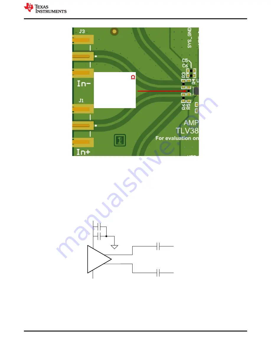
Additionally, the pads from R4 and R5 can be used to solder a 100-Ω termination resistor for LVDS input signals.
Option for 100
differential
resistor for
LVDS input
signals
Figure 6-3. Configuration for LVDS Inputs Using the Unused Pads of R4 and R5
6.3 Outputs
C10 and C11 are installed with 0.1-uF capacitors. If a 100-Ω differential probe is unavailable to measure the
LVDS output, these capacitors allow for the AC portion of the signal to be seen on a 50-Ω terminated scope.
Keep in mind that any duty cycle other than 50% will result in a DC portion of the signal that is not halfway
between V
OH
and V
OL
. As mentioned earlier, this is because of the charging and discharging of the capacitors.
A higher duty cycle will result in a higher DC output voltage because the capacitors are charging more than they
are discharging.
+
–
GND
V
CC
V
EE_Out
C10
0.1uF
C11
0.1uF
OUT+
OUT-
Figure 6-4. Output Side Schematic
If equipment is available to measure the LVDS output with a respect to the 100-Ω resistor or with a differential
probe, then C10 and C11 can be replaced with 0-Ω resistors to keep the DC integrity of the output signal.
Board Setup
SNOU184 – NOVEMBER 2021
TLV3801EVM User’s Guide
9
Copyright © 2021 Texas Instruments Incorporated


