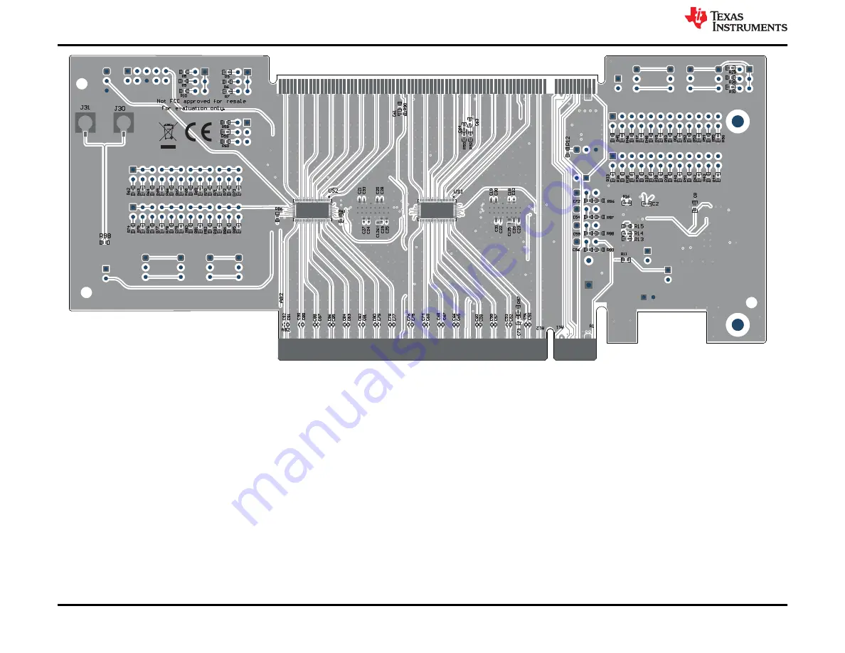
Figure 5-2. Bottom Layer
Schematics
www.ti.com
22
DS160PR810EVM-RSC Evaluation Module (EVM)
SNLU273 – DECEMBER 2020
Submit Document Feedback
Copyright © 2020 Texas Instruments Incorporated
Page 1: ...ototyping Figure 1 1 DS160PR810EVM RSC Top Side View Table of Contents 1 Introduction 2 1 1 Features 2 1 2 Applications 2 2 Description 3 2 1 DS160PR810 4 Level I O Control Inputs 3 2 2 DS160PR810 Mod...
Page 2: ...mount connector attached to the other end of the board 1 1 Features PCIe x16 Riser Card option with four 8 channel unidirectional linear redrivers operating at rates up to 25 Gbps Linear equalization...
Page 3: ...D L1 13 k to GND L2 59 k to GND L3 Float 2 2 DS160PR810 Modes of Operation Each DS160PR810 can be configured to operate in either Pin Mode SMBus with I2C Slave Mode or SMBus with I2C Master Mode The m...
Page 4: ...ssigned to the device by placing external resistor straps on the EQ0_0 ADDR1 and EQ1_0 ADDR0 pins as shown in Table 2 3 When multiple DS160PR810 devices are on the same SMBus interface bus each channe...
Page 5: ...EQ INDEX EQ1 PIN LEVEL EQ0 PIN LEVEL CTLE BOOST AT 4 GHz dB CTLE BOOST AT 8 GHz dB 0 L0 L0 0 25 0 5 1 L0 L1 2 0 4 0 2 L0 L2 2 5 5 0 3 L0 L3 3 0 6 0 4 L1 L0 4 0 7 0 5 L1 L1 4 5 7 5 6 L1 L2 5 0 8 0 7 L1...
Page 6: ...detections L L2 PCI Express RX detection state machine is enabled Recommended for PCI Express use cases Pre Detect Hi Z Post Detect 50 Outputs poll every approximate 150 s until 2 consecutive valid R...
Page 7: ...Tie PCIe system PRSNT signal to PWDN using J6 for the PWDN control optional for PCIe use case J5 3x1 Header Access point to the WP write protect pin of the onboard EEPROM devices WP tied to GND I2C A...
Page 8: ...ring EQ0_1 pin of Bank 1 of DS1 device Use pins 13 18 for configuring EQ0_0 pin of Bank 0 of DS2 device Use pins 19 24 for configuring EQ0_1 pin of Bank 1 of DS2 device SMBus I2C Modes ADDR0 controls...
Page 9: ...n of Bank 1 of US1 device Use pins 13 18 for configuring EQ0_0 pin of Bank 0 of US2 device Use pins 19 24 for configuring EQ0_1 pin of Bank 1 of US2 device SMBus I2C Modes ADDR0 controls for each upst...
Page 10: ...ts in the following arrangement On J15 connector place shunts in L0 locations for all downstream devices DS1_0 and DS2_0 DS1_1 and DS2_1 are a Don t Care On J16 connector place shunts in L0 locations...
Page 11: ...2 1 SigCon Architect DS160PR810 High Level Page www ti com Description SNLU273 DECEMBER 2020 Submit Document Feedback DS160PR810EVM RSC Evaluation Module EVM 11 Copyright 2020 Texas Instruments Incorp...
Page 12: ...ver EVM 10 WHQGHU DUG Server Motherboard PCIe Gen 4 CPU 8 WHQGHU DUG 6 WHQGHU DUG Figure 3 1 Example Test Setup Figure 3 2 is a typical test result achieved with a system shown in Figure 3 1 As the re...
Page 13: ..._P PER4_N PER5_P PER5_N PER6_P PER6_N PER7_P PER7_N PER8_P PER8_N PER9_P PER9_N PER10_P PER10_N PER11_P PER11_N PER12_P PER12_N PER13_P PER13_N PER14_P PER14_N PER15_P PER15_N SMCLK SMDAT JTAG1 WAKE C...
Page 14: ...2 PRSNT2_3_C PRSNT2_3 PRSNT2_4_C PRSNT2_4 PWDN SDA SCL SDA SCL GND 1 2 3 4 5 6 7 8 9 10 J3 SW1 4 70k R11 J6 1 2 3 J4 1 2 3 J7 1 2 3 J8 1 2 3 J9 1 2 3 J10 GND 3_3V_REG 3_3V_REG 3_3V_REG 3_3V_REG 3_3V_R...
Page 15: ...FSEL 32 VSEL 33 MODE 34 PGOOD 35 ILIM 36 RESV_TRK 37 RSN 38 RSP 39 VOSNS 40 PAD 41 TPS548B22RVFR U3 100uF C11 100uF C10 10 0k R27 5 76k R28 100k R21 105k R25 165k R20 37 4k R22 42 2k R24 2 05k R26 6 8...
Page 16: ...3 R91 RSVD2 1pF C63 43 R92 1pF C64 43 R93 RSVD4 1pF C70 43 R94 RSVD 1pF C71 43 R95 CLKREQ 1pF C72 43 R96 PRSNT2_1 1pF C73 43 R97 RSVD1 1pF C54 43 R87 PRSNT2_2 1pF C55 43 R88 PRSNT2_3 1pF C56 43 R89 PR...
Page 17: ...T6_C_N PET7_C_P PET7_C_N 3_3V_REG MODE GAIN_DS PWDN PWDN READ_EN_N 3_3V_REG 4 70k R32 ALL_DONE_N_DS1 GAIN0_SDA_DS1 RX_DET_SCL_DS1 GAIN0_SDA_DS1 GAIN_DS SDA RX_DET_SCL_DS1 RX_DET SCL EQ1_0_AD1_DS1 EQ0_...
Page 18: ..._US PWDN PWDN 3_3V_REG 4 70k R61 ALL_DONE_N_US1 GAIN0_SDA_US1 RX_DET_SCL_US1 EQ1_0_AD1_US1 EQ0_0_AD0_US1 EQ1_1_US1 EQ0_1_US1 ALL_DONE_N_DS 3_3V_REG VCC 6 VCC 18 VCC 38 VCC 50 RX0N 2 RX0P 1 RX1N 5 RX1P...
Page 19: ...N PET11_C_P PET11_C_N PET12_C_P PET12_C_N PET13_C_P PET13_C_N PET14_C_P PET14_C_N PET15_C_P PET15_C_N PRSNT2_4_C RSVD RSVD5 12V 3_3V 12V 3_3V 3_3VAUX GND GND GND GND GND GND GND GND GND GND GND GND GN...
Page 20: ...ified Variant Label Table Variant Label Text 001 DS160PR810EVM RSC LOGO PCB FCC disclaimer LOGO PCB WEEE logo SH J8 SH J1 SH J6 SH J4 SH J2 SH J5 SH J7 SH J3 SH J14 SH J9 SH J15 SH J10 SH J16 SH J11 S...
Page 21: ...and Figure 5 2 illustrate the EVM board layouts Figure 5 1 Top Layer www ti com Schematics SNLU273 DECEMBER 2020 Submit Document Feedback DS160PR810EVM RSC Evaluation Module EVM 21 Copyright 2020 Texa...
Page 22: ...Figure 5 2 Bottom Layer Schematics www ti com 22 DS160PR810EVM RSC Evaluation Module EVM SNLU273 DECEMBER 2020 Submit Document Feedback Copyright 2020 Texas Instruments Incorporated...
Page 23: ...00 uF 6 3 V 20 X5R 0805 0805 GRM21BR60J107M MuRata C12 1 47uF CAP CERM 47 uF 6 3 V 20 X5R 0805 0805 GRM219R60J476ME44D MuRata C13 1 10uF CAP CERM 10 uF 6 3 V 10 X5R 0805 0805 C0805C106K9PAC Kemet C14...
Page 24: ...Fastener Supply J1 J2 J14 J21 4 Header 100mil 3x2 Gold TH 3x2 Header TSW 103 07 G D Samtec J3 1 Header 100mil 5x2 Gold TH 5x2 Header TSW 105 07 G D Samtec J4 J5 J7 J8 J9 J10 J17 J18 J19 J20 J24 J25 J2...
Page 25: ...0402 0402 CRCW040242K2FKED Vishay Dale R25 1 105k RES 105 k 1 0 063 W AEC Q200 Grade 0 0402 0402 CRCW0402105KFKED Vishay Dale R26 1 2 05k RES 2 05 k 1 0 063 W AEC Q200 Grade 0 0402 0402 CRCW04022K05FK...
Page 26: ...Gate With 3 State Outputs PW0014A LARGE T and R PW0014A SN74LVC125APWRG3 Texas Instruments U3 1 1 5 V to 16 V VIN 4 5 V to 22 V VDD 25 A SWIFT Synchronous Step Down Converter with Full Differential S...
Page 27: ...160PR810 Programming Guide 3 Texas Instruments Understanding EEPROM Programming for DS160PR810 PCI Express 4 0 Linear Redriver 4 Texas Instruments CEM2SLIMSAS EVM Evaluation Module EVM User s Guide ww...
Page 28: ...ther than TI b the nonconformity resulted from User s design specifications or instructions for such EVMs or improper system design or c User has not paid on time Testing and other quality control tec...
Page 29: ...These limits are designed to provide reasonable protection against harmful interference in a residential installation This equipment generates uses and can radiate radio frequency energy and if not in...
Page 30: ...instructions set forth by Radio Law of Japan which includes but is not limited to the instructions below with respect to EVMs which for the avoidance of doubt are stated strictly for convenience and s...
Page 31: ...any interfaces electronic and or mechanical between the EVM and any human body are designed with suitable isolation and means to safely limit accessible leakage currents to minimize the risk of electr...
Page 32: ...R DAMAGES ARE CLAIMED THE EXISTENCE OF MORE THAN ONE CLAIM SHALL NOT ENLARGE OR EXTEND THIS LIMIT 9 Return Policy Except as otherwise provided TI does not offer any refunds returns or exchanges Furthe...
Page 33: ...e resources are subject to change without notice TI grants you permission to use these resources only for development of an application that uses the TI products described in the resource Other reprod...