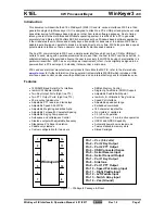
SOC0
ADCCLK
ADCRESULT 0
S/H Window Pulse to Core
ADCCTL 1.INTPULSEPOS
ADCSOCFLG 1.SOC0
ADCINTFLG .ADCINTx
SOC1
SOC2
9
15
22
24
37
2
0
Result 0 Latched
ADCSOCFLG 1.SOC1
ADCSOCFLG 1.SOC2
ADCRESULT 1
EOC0 Pulse
EOC1 Pulse
Conversion 0
13 ADC Clocks
Minimum
7 ADCCLKs
6
ADCCLKs
Conversion 1
13 ADC Clocks
Minimum
7 ADCCLKs
2 ADCCLKs
1 ADCCLK
Analog Input
SOC1 Sample
Window
SOC0 Sample
Window
SOC2 Sample
Window
(A)
Analog-to-Digital Converter (ADC)
898
SPRUH22I – April 2012 – Revised November 2019
Copyright © 2012–2019, Texas Instruments Incorporated
Analog Subsystem
10.3.13 ADC Timings
Figure 10-49. Timing Example For Sequential Mode / Late Interrupt Pulse
A
Result 0 latched on this cycle does not include the additional cycles required for the C28x and M3 subsystems to read
the ADC result registers using the ACIB.


