


CC112X/CC1175
SWRU295C
Page 8 of 108
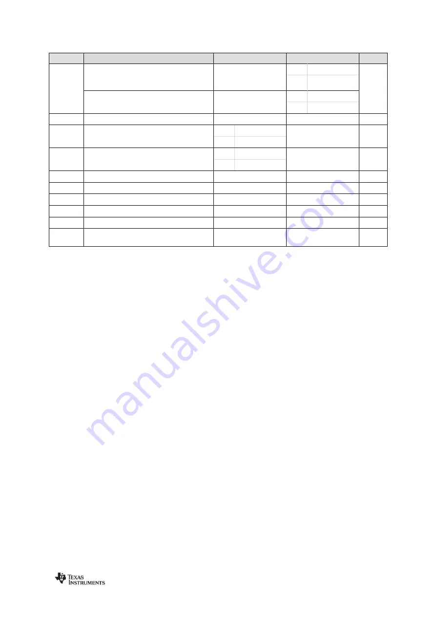
Parameter
Description
Min
Max
Units
f
SCLK
SCLK frequency read/write access
Note: 100 or 125 ns delay between consecutive data bytes
must be added during burst write access to the configuration
registers depending on f
XOSC
(40 or 32 MHz)
-
10
f
XOSC
= 40 MHz
MHz
8
f
XOSC
= 32 MHz
SCLK frequency read access extended
memory
-
7.7
f
XOSC
= 40 MHz
6.1
f
XOSC
= 32 MHz
t
sp
CSn low to positive edge on SCLK
50
-
ns
t
ch
Clock high
47.5
f
XOSC
= 40 MHz
-
ns
60
f
XOSC
= 32 MHz
t
cl
Clock low
47.5
f
XOSC
= 40 MHz
-
ns
60
f
XOSC
= 32 MHz
t
rise
Clock rise time
-
40
ns
t
fall
Clock fall time
-
40
ns
t
sd
Setup data before a positive edge on SCLK
10
-
ns
t
hd
Hold data after positive edge on SCLK
10
-
ns
t
ns
Negative edge on SCLK to CSn high.
200
-
ns
CSn high time, time from CSn has been pulled
high until it can be pulled low again
50
ns
Table 1: SPI Timing Requirements
When CSn is pulled low, the MCU must wait until
CC112X
SO pin goes low before starting to transfer
the header byte. This indicates that the crystal is stable. Unless the chip was just reset or was in
SLEEP or XOFF state, or the XOSC configuration has been altered, the SO pin will always go low
immediately after pulling CSn low.
Registers with consecutive addresses can be accessed in an efficient way by setting the burst bit (B)
in the header byte. The address bits (A
5
- A
0
) set the start address in an internal address counter. This
counter is incremented by one each new byte (every 8 clock pulses). The burst access is either a
read or write, and must be terminated by setting CSn high.
If a single register shall be accessed multiple times (e.g.
for custom frequency modulation, see Section 4.1.3), the
be set to 0. In this mode the address counter will not increment in burst mode, and it is possible to
read/write the same register repeatedly without address overhead.
Table 3 gives an overview of the different SPI access types possible.
3.1.2
Chip Status Byte
When the header byte, data byte, or command strobe is sent on the SPI interface, the chip status byte
is sent by the
CC112X
on the SO pin. The status byte contains key status signals, useful for the MCU.
The first bit, S
7
signal and this signal must go low before the first positive edge of
signal indicates that the crystal is stable.
S
6
, S
5
, and S
4
value which reflects the state of the chip. In IDLE state the XOSC
and power to the digital core are on and all other modules are in power down. Unless otherwise
stated, registers should not be changed unless the chip is in this state.
Table 2 gives a status byte summary.