background image

Clock provided by CC1020

FSK modulating signal (Manchester
encoded), internal in CC1020

Data provided by microcontroller

Transmitter side:

Clock provided by CC1020

Demodulated signal (Manchester
encoded), internal in CC1020

Data provided by CC1020

DCLK

DIO

“RF”

“RF”

DCLK

DIO

Receiver side:

Clock provided by CC1020

FSK modulating signal (NRZ),
internal in CC1020

Data provided by microcontroller

Transmitter side:

Clock provided by CC1020

Demodulated signal (NRZ),
internal in CC1020

Data provided by CC1020

DCLK

DIO

“RF”

“RF”

DCLK

DIO

Receiver side:

Clock provided by CC1020

FSK modulating signal (NRZ),
internal in CC1020

Data provided by microcontroller

Transmitter side:

Clock provided by CC1020

Demodulated signal (NRZ),
internal in CC1020

Data provided by CC1020

DCLK

DIO

“RF”

“RF”

DCLK

DIO

Receiver side:

CC1020

www.ti.com

SWRS046H – NOVEMBER 2006 – REVISED MARCH 2015

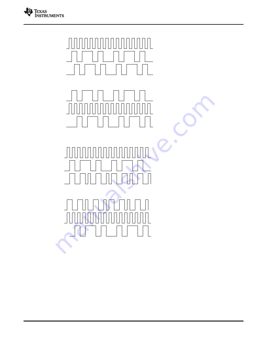
Figure 5-6. Synchronous NRZ Mode (SEP_DI_DO = 0)

Figure 5-7. Synchronous Manchester Encoded Mode (SEP_DI_DO = 0)

Copyright © 2006–2015, Texas Instruments Incorporated

Detailed Description

23

Submit Documentation Feedback

Product Folder Links:

CC1020

Summary of Contents for CC1020

Page 1: ...kHz Home Automation 402 424 426 429 433 447 449 469 Low Power Telemetry 868 915 960 MHz ISM SRD Band Systems 1 3 Description CC1020 is a true single chip UHF transceiver designed for very low power and very low voltage wireless applications The circuit is mainly intended for the ISM Industrial Scientific and Medical and SRD Short Range Device frequency bands at 402 424 426 429 433 447 449 469 868 ...

Page 2: ...DC RF_OUT R_BIAS XOSC_Q1 XOSC_Q2 PDO XOSC VC CHP_OUT LNA 2 0 90 2 0 90 2 Multiplexer Multiplexer PA_EN LNA_EN PCLK PDI PSEL CC1020 SWRS046H NOVEMBER 2006 REVISED MARCH 2015 www ti com 1 4 Functional Block Diagram Figure 1 1 shows the system block diagram of the CC1020 device Figure 1 1 Functional Block Diagram 2 Device Overview Copyright 2006 2015 Texas Instruments Incorporated Submit Documentatio...

Page 3: ... 5 RF Receive 9 5 21 Antenna Considerations 61 4 6 RSSI Carrier Sense 12 5 22 Configuration Registers 62 4 7 Intermediate Frequency IF 12 6 Applications Implementation and Layout 83 4 8 Crystal Oscillator 13 6 1 Application Information 83 4 9 Frequency Synthesizer 14 6 2 Design Requirements 85 4 10 Digital Inputs and Outputs 15 6 3 PCB Layout Recommendations 86 4 11 Current Consumption 16 7 Device...

Page 4: ...anges from Revision F January 2006 to Revision G Page Converted document to new TI standards 1 Added Thermal Resistance Characteristics for VQFNP Package 16 Changed Register table format to new TI standards 62 Changes from January 19 2015 to February 19 2015 Page Updated RUZ package to RSS 87 4 Revision History Copyright 2006 2015 Texas Instruments Incorporated Submit Documentation Feedback Produc...

Page 5: ... I O 5 DVDD Power digital Power supply 3 V typical for digital modules and digital I O 6 DGND Ground digital Ground connection 0 V for digital modules substrate Clock for data in both receive and transmit mode 7 DCLK Digital output Can be used as receive data output in asynchronous mode Data input in transmit mode data output in receive mode 8 DIO Digital input output Can also be used to start pow...

Page 6: ...ers prescaler and first PA 22 AVDD Power analog stage 23 AVDD Power analog Power supply 3 V typical for VCO 24 VC Analog input VCO control voltage input from external loop filter 25 AGND Ground analog Ground connection 0 V for analog modules guard 26 AD_REF Power analog 3 V reference input for ADC 27 AVDD Power analog Power supply 3 V typical for charge pump and phase detector 28 CHP_OUT Analog ou...

Page 7: ...cation for Nonhermetic Solid State Surface Mount Devices 4 2 ESD Ratings VALUE UNIT All pads except RF 1 kV Human Body Model HBM per Electrostatic discharge ESD ANSI ESDA JEDEC JS001 1 2 VESD RF Pads 0 4 kV performance Charged device Model CDM 250 V 1 JEDEC document JEP155 states that 500 V HBM allows safe manufacturing with a standard ESD control process Manufacturing with less than 500 V HBM is ...

Page 8: ... 2nd harmonic 433 MHz 50 dBc 10 dBm Harmonics are measured as EIRP 3rd harmonic 433 MHz 50 dBc values according to EN 300 220 The 10 dBm Harmonics antenna SMAFF 433 and SMAFF 868 radiated CW 2nd harmonic 868 MHz from R W Badland plays a part in 50 dBc 5 dBm attenuating the harmonics 3rd harmonic 868 MHz 50 dBc 5 dBm 12 5 kHz channel spacing For 12 5 kHz channel spacing ACP is 46 dBc 433 MHz measur...

Page 9: ...ere performed using the two layer PCB CC1020EMX reference design See Figure 6 1 The electrical specifications given for 868 MHz are also applicable for 902 to 928 MHz TA 25 C AVDD DVDD 3 0 V fC 14 7456 MHz if nothing else stated PARAMETER MIN TYP MAX UNIT CONDITION 12 5 kHz channel spacing optimized Sensitivity is measured with PN9 114 dBm selectivity 2 025 kHz freq deviation sequence at BER 10 3 ...

Page 10: ...ration will I Q gain and phase 49 52 dB depend on temperature and supply calibrated voltage Refer to Section 5 9 6 12 5 kHz channel spacing 433 MHz 41 dB Wanted signal 3 dB above the sensitivity level CW jammer is 25 kHz channel spacing 433 MHz 41 dB swept in 12 5 kHz 25 kHz steps to Selectivity 2 within 1 MHz from wanted channel 25 kHz channel spacing 868 MHz 39 dB BER 10 3 Adjacent channel and i...

Page 11: ...equency resides between VCO leakage 64 dBm 1608 and 1880 MHz 9 kHz to 1 GHz 60 dBm Complying with EN 300 220 FCC CFR47 part 15 and ARIB STD T96 Spurious emission Spurious emissions can be radiated CW 1 to 4 GHz 60 dBm measured as EIRP values according to EN 300 220 433 MHz 58 j10 Ω Receive mode See Section 5 11 for Input impedance details 868 MHz 54 j22 Ω 433 MHz 14 dB Using application circuit ma...

Page 12: ...carrier sense level 110 dBm FM jammer 1 kHz sine 2 5 kHz deviation at adjacent channel Adjacent channel carrier Adjacent channel carrier sense is measured sense 25 kHz channel spacing 72 dBm by applying a signal on the adjacent channel and observe at which level carrier sense is indicated At carrier sense level 110 dBm 100 MHz to Spurious carrier sense 70 dBm 2 GHz Adjacent channel and image chann...

Page 13: ... 8 to 19 6 MHz 16 pF 12 16 16 pF recommended 4 9152 MHz 12 pF load 1 55 ms 7 3728 MHz 12 pF load 1 0 ms 9 8304 MHz 12 pF load 0 90 ms Crystal oscillator start up time 14 7456 MHz 16 pF load 0 95 ms 17 2032 MHz 12 pF load 0 60 ms 19 6608 MHz 12 pF load 0 63 ms The external clock signal must be connected to XOSC_Q1 using a DC block 10 nF Set XOSC_BYPASS 0 in External clock signal drive sine wave 300...

Page 14: ...r 101 dBc Hz given in Table 6 2 The phase noise will 25 kHz channel spacing be higher for larger PLL loop filter At 100 kHz offset from carrier 109 dBc Hz bandwidth At 1 MHz offset from carrier 118 dBc Hz 12 5 kHz channel spacing 433 MHz 2 7 kHz After PLL and VCO calibration The PLL PLL loop bandwidth loop bandwidth is programmable 25 kHz channel spacing 868 MHz 8 3 kHz 12 5 kHz channel spacing 43...

Page 15: ... be 350 µA Logic 1 input current N A 1 µA Input signal equals VDD TX mode minimum time DIO must be ready before the DIO setup time 20 ns positive edge of DCLK Data should be set up on the negative edge of DCLK TX mode minimum time DIO must be held after the DIO hold time 10 ns positive edge of DCLK Data should be set up on the negative edge of DCLK Serial interface PCLK PDI PDO and PSEL timing See...

Page 16: ... and synthesizer 7 5 mA crystal 4 12 Thermal Resistance Characteristics for VQFNP Package NAME DESCRIPTION C W 1 2 RθJC top Junction to case top 16 2 RθJB Junction to board 6 9 RθJA Junction to free air 30 7 PsiJT Junction to package top 0 2 PsiJB Junction to board 6 9 RθJC bottom Junction to case bottom 1 0 1 C W degrees Celsius per watt 2 These values are based on a JEDEC defined 2S2P system wit...

Page 17: ...nchronized data clock is available at the DCLK pin RSSI is available in digital format and can be read via the serial interface The RSSI also features a programmable carrier sense indicator In transmit mode the synthesized RF frequency is fed directly to the power amplifier PA The RF output is frequency shift keyed FSK by the digital bit stream that is fed to the DIO pin Optionally a Gaussian filt...

Page 18: ...al RSSI and carrier sense FSK GFSK and OOK modulation 5 3 1 Configuration Software TI provides users of CC1020 with a software program SmartRF Studio Windows interface that generates all necessary CC1020 configuration data based on the user s selections of various parameters These hexadecimal numbers will then be the necessary input to the microcontroller for the configuration of CC1020 In additio...

Page 19: ...an be saved if PDI and PDO are connected together and a bi directional pin is used at the microcontroller The microcontroller pins connected to PDI PDO and PCLK can be used for other purposes when the configuration interface is not used PDI PDO and PCLK are high impedance inputs as long as PSEL is not activated active low PSEL has an internal pullup resistor and should be left open tri stated by t...

Page 20: ...ts are then transferred D7 0 During address and data transfer the PSEL Program Select must be kept low See Figure 5 4 The timing for the programming is also shown in Figure 5 4 with reference to Table 5 1 The clocking of the data on PDI is done on the positive edge of PCLK Data should be set up on the negative edge of PCLK by the microcontroller When the last bit D0 of the 8 data bits has been loa...

Page 21: ...efore the positive edge of PCLK The minimum time data must be held at PDI THD PDI hold time 25 ns after the positive edge of PCLK Trise Rise time 100 ns The maximum rise time for PCLK and PSEL Tfall Fall time 100 ns The maximum fall time for PCLK and PSEL 1 The setup and hold times refer to 50 of VDD The rise and fall times refer to 10 90 of VDD The maximum load that this table is valid for is 20 ...

Page 22: ... Manchester code The encoding is done by CC1020 In this mode the effective bit rate is half the baud rate due to the coding As an example 4 8 kBaud Manchester encoded data corresponds to 2 4 kbps In receive mode CC1020 performs the synchronization and provides received data clock at DCLK and data at DIO CC1020 performs the decoding and NRZ data is presented at DIO The data should be clocked into t...

Page 23: ... CC1020 FSK modulating signal NRZ internal in CC1020 Data provided by microcontroller Transmitter side Clock provided by CC1020 Demodulated signal NRZ internal in CC1020 Data provided by CC1020 DCLK DIO RF RF DCLK DIO Receiver side Clock provided by CC1020 FSK modulating signal NRZ internal in CC1020 Data provided by microcontroller Transmitter side Clock provided by CC1020 Demodulated signal NRZ ...

Page 24: ... Connect to UART RXD Demodulated signal NRZ internal in CC1020 DIO is not used in receive mode Used only as data input in transmit mode DCLK DIO RF RF DCLK DIO Receiver side CC1020 SWRS046H NOVEMBER 2006 REVISED MARCH 2015 www ti com Figure 5 8 Transparent Asynchronous UART Mode SEP_DI_DO 1 Figure 5 9 Manchester Encoding 5 7 Data Rate Programming The data rate baud rate is programmable and depends...

Page 25: ...8304 12 288 14 7456 17 2032 19 6608 0 45 X X 0 5 X 0 6 X X X X X X X 0 9 X X 1 X 1 2 X X X X X X X 1 8 X X 2 X 2 4 X X X X X X X 3 6 X X 4 X 4 096 X X 4 8 X X X X X X X 7 2 X X 8 X 8 192 X X 9 6 X X X X X X X 14 4 X X 16 X 16 384 X X 19 2 X X X X X X X 28 8 X X 32 X 32 768 X X 38 4 X X X X X X X 57 6 X X 64 X 65 536 X 76 8 X X X X X X X 115 2 X X 128 X 153 6 X X X X X Copyright 2006 2015 Texas Ins...

Page 26: ...n 3 in the frequency band 804 to 960 MHz 3 The BANDSELECT bit in the ANALOG register controls the frequency band used BANDSELECT 0 gives 402 to 470 MHz and BANDSELECT 1 gives 804 to 960 MHz The reference frequency is the crystal oscillator clock frequency divided by REF_DIV 3 bits in the CLOCK_A or CLOCK_B register a number between 1 and 7 as shown in Equation 4 4 FSK frequency deviation is progra...

Page 27: ...ed assuming low frequency deviations and low data rates Large offsets however from the nominal IF frequency will give an un symmetric filtering variation in group delay and different attenuation of the signal resulting in decreased sensitivity and selectivity See AN022 CC1020 Crystal Frequency Selection SWRA070 for more details For IF frequencies other than 300 to 320 kHz and for high frequency de...

Page 28: ...ceiver channel filter bandwidth The 6 dB bandwidth is given by Equation 17 17 Where the IF frequency is set to 307 2 kHz In SmartRF Studio the user specifies the channel spacing and the channel filter bandwidth is set according to Table 5 5 For narrowband systems with channel spacings of 12 5 and 25 kHz the channel filter bandwidth is 12 288 kHz and 19 2 kHz respectively to comply with ARIB STD T6...

Page 29: ...parison level The RXDEV_X 1 0 and RXDEV_M 3 0 in the AFC_CONTROL register are used to set the expected deviation of the incoming signal Once a shift in the received frequency larger than the expected deviation is detected a bit transition is recorded and the average value to be used by the data slicer is calculated The minimum number of transitions required to calculate a slicing level is 3 That i...

Page 30: ...E DEVIATION SPACING FILTER BW MANCHESTER kBaud kHz NRZ MODE UART MODE kHz MODE 2 4 optimized 12 5 2 025 9 6 115 118 115 sensitivity 1 2 4 optimized 12 5 2 025 12 288 112 114 112 selectivity 1 4 8 25 2 475 19 2 112 112 112 9 6 50 4 95 25 6 110 111 110 19 2 100 9 9 51 2 107 108 107 38 4 150 19 8 102 4 104 104 104 76 8 200 36 0 153 6 101 101 101 153 6 500 72 0 307 2 96 97 96 1 Optimized selectivity i...

Page 31: ... the channel filter bandwidth used due to different VGA settings Figure 5 11 and Figure 5 12 show typical plots of RSSI reading as a function of input power for different channel spacings See Section 5 9 5 for a list of channel filter bandwidths corresponding to the various channel spacings Refer to AN030 CC1020 1021 Received Signal Strength Indicator SWRA062 for further details The method shown i...

Page 32: ...ise floor For best RSSI accuracy use AGC_AVG 1 0 11 during image rejection calibration RSSI value is averaged over 16 filter output samples The RSSI register update rate then equals the receiver channel bandwidth set in FILTER register divided by 8 as the filter output rate is twice the receiver channel bandwidth This gives the minimum waiting time between RSSI register reads 0 5 ms is used below ...

Page 33: ...ast 3 ms Measure signal strength Y2 as filtered average of 8 reads from RSSI register with 0 5 ms of delay between each RSSI read 25 Write XG DX to GAIN_COMP register 26 Wait at least 3 ms Measure signal strength Y1 as filtered average of 8 reads from RSSI register with 0 5 ms of delay between each RSSI read 27 Write XG 2 DX to GAIN_COMP register 28 Wait at least 3 ms Measure signal strength Y0 as...

Page 34: ...l loop ensures that the ADC operates inside its dynamic range by using an analog digital feedback loop The maximum VGA gain is programmed by the VGA_SETTING 4 0 in the VGA3 register The VGA gain is programmed in approximately 3 dB LSB The VGA gain should be set so that the amplified thermal noise from the front end balance the quantization noise from the ADC Therefore the optimum maximum VGA gain ...

Page 35: ...nts are expected due to DC offsets in the VGA At the sensitivity limit the VGA gain is set by VGA_SETTING In order to optimize selectivity this gain should not be set higher than necessary The SmartRF Studio software gives the settings for VGA1 to VGA4 registers For reference the following method can be used to find the AGC settings 1 Disable AGC and use maximum LNA2 gain by writing BFh to the VGA...

Page 36: ...ecause the AGC settling time can be reduced for data rates lower than 76 8 kBaud by using a wider receiver channel filter bandwidth that is larger ChBW 5 9 10 Preamble Length and Sync Word The rules for choosing a good sync word are as follows 1 The sync word should be significantly different from the preamble 2 A large number of transitions is good for the bit synchronization or clock recovery Eq...

Page 37: ...be powered up automatically by a wake up signal and will then check for a carrier signal carrier sense If carrier sense is not detected it returns to power down mode A flow chart for automatic power up sequencing is shown in Figure 5 16 The automatic power up sequencing mode is selected when PD_MODE 1 0 11 in the MAIN register When the automatic power up sequencing mode is selected the functionali...

Page 38: ...ilter clock FILTER_CLK ffilter_clock 2 ChBW where ChBW is defined in Section 5 9 2 2 ADC clock ADC_CLK where ADC_DIV 2 0 is set in the MODEM register Figure 5 16 Automatic Power up Sequencing Flow Chart 5 9 13 Automatic Frequency Control CC1020 has a built in feature called AFC Automatic Frequency Control that can be used to compensate for frequency drift The average frequency offset of the receiv...

Page 39: ... domain and the 3 dB cut off frequency is 0 6 times the programmed Baud rate Thus for audio the minimum programmed Baud rate should be approximately 7 2 kBaud The GAUSS_FILTER resolution decreases with increasing baud rate A accumulate and dump filter can be implemented in the µC to improve the resolution Note that each GAUSS_FILTER reading should be synchronized to the MODEM_CLK As an example acc...

Page 40: ...able by the 8 bit PA_POWER register Figure 5 20 and Figure 5 21 show the output power and total current consumption as a function of the PA_POWER register setting It is more efficient in terms of current consumption to use either the lower or upper 4 bits in the register to control the power as shown in Figure 5 20 and Figure 5 21 However the output power can be controlled in finer steps using all...

Page 41: ... com SWRS046H NOVEMBER 2006 REVISED MARCH 2015 Figure 5 20 Typical Output Power and Current Consumption 433 MHz Figure 5 21 Typical Output Power and Current Consumption 433 MHz 5 10 3 TX Data Latency The transmitter will add a delay due to the synchronization of the data with DCLK and further clocking into the modulator The user should therefore add a delay equivalent to at least 2 bits after the ...

Page 42: ...ng network is shown in Figure 5 22 Component values for various frequencies are given in Table 5 8 Component values for other frequencies can be found using the SmartRF Studio software As can be seen from Figure 5 22 and Table 5 8 the 433 MHz network utilizes a T type filter while the 868 915 MHz network has a π type filter topology It is important to remember that the physical layout and the comp...

Page 43: ...C71 DNM 1 8 2 pF 5 NP0 0402 8 2 pF 5 NP0 0402 C72 4 7 pF 5 NP0 0402 8 2 pF 5 NP0 0402 8 2 pF 5 NP0 0402 L1 33 nH 5 0402 82 nH 5 0402 82 nH 5 0402 L2 22 nH 5 0402 3 6 nH 5 0402 3 6 nH 5 0402 L70 47 nH 5 0402 5 1 nH 5 0402 5 1 nH 5 0402 L71 39 nH 5 0402 0 Ω resistor 0402 0 Ω resistor 0402 R10 82 Ω 5 0402 82 Ω 5 0402 82 Ω 5 0402 1 DNM Do Not Mount Figure 5 23 Typical LNA Input Impedance 200 to 1000 M...

Page 44: ... Typical Optimum PA Load Impedance 433 MHz Table 5 9 Impedances at the First 5 Harmonics 433 MHz Matching Network FREQUENCY REAL IMAGINARY MHz Ohms Ohms 433 54 44 866 20 173 1299 288 563 1732 14 123 2165 5 66 44 Detailed Description Copyright 2006 2015 Texas Instruments Incorporated Submit Documentation Feedback Product Folder Links CC1020 ...

Page 45: ...Ohms 868 15 24 915 20 35 1736 1 5 18 1830 1 7 22 2604 3 2 44 2745 3 6 45 5 12 Frequency Synthesizer 5 12 1 VCO Charge Pump and PLL Loop Filter The VCO is completely integrated and operates in the 1608 to 1920 MHz range A frequency divider is used to get a frequency in the UHF range 402 to 470 and 804 to 960 MHz The BANDSELECT bit in the ANALOG register selects the frequency band Copyright 2006 201...

Page 46: ...gain and bandwidth higher charge pump current when VCO sensitivity is lower Equation 25 through Equation 29 can be used for calculating PLL loop filter component values see Figure 6 1 for a desired PLL loop bandwidth BW 25 26 27 28 29 Define a minimum PLL loop bandwidth as shown in Equation 30 30 If BWmin Baud rate 3 then set BW BWmin and if BWmin Baud rate 3 then set BW Baud rate 3 in Equation 25...

Page 47: ... setting the CAL_START bit in the CALIBRATE register The calibration result is stored internally in the chip and is valid as long as power is not turned off If large supply voltage drops typically more than 0 25 V or temperature variations typically more than 40 C occur after calibration a new calibration should be performed The nominal VCO control voltage is set by the CAL_ITERATE 2 0 bits in the...

Page 48: ...libration for RX and TX frequency is illustrated in Figure 5 26 The same algorithm is applicable for dual calibration if CAL_DUAL 1 Refer to Application Note AN023 CC1020 MCU Interfacing SWRA069 which includes example source code for single calibration TI recommends that single calibration be used for more robust operation There is a small but finite possibility that the PLL self calibration will ...

Page 49: ...S_PD 0 RESET_N 1 Write FREQ_A FREQ_B VCO CLOCK_A and CLOCK_B registers PLL_BW 174 16log2 fref 7 126 Start single calibration Start single calibration Write CALIBRATE register B4h Start calibration fref is the reference frequency in MHz Yes Read STATUS register and wait until LOCK_CONTINUOUS 1 Read STATUS register and wait until CAL_COMPLETE 1 Calibration OK No CC1020 www ti com SWRS046H NOVEMBER 2...

Page 50: ... frequency when going from RX to TX mode or vice versa The PLL lock time depends on the PLL loop filter bandwidth Table 5 13 gives the PLL lock time for different PLL loop filter bandwidths Table 5 13 Typical PLL Lock Time to Within 10 of Channel Spacing for Different Loop Filter Bandwidths 1 PLL LOCK TIME µs C6 C7 C8 R2 R3 Comment nF pF pF kΩ kΩ 1 2 3 Up to 4 8 kBaud data rate 12 5 kHz 220 8200 2...

Page 51: ...s a typical sequence for activating RX and TX mode from power down mode for minimum power consumption NOTE PSEL should be tri stated or set to a high level during power down mode in order to prevent a trickle current from flowing in the internal pullup resistor Application Note AN023 CC1020 MCU Interfacing SWRA069 includes example source code TI recommends resetting the CC1020 by clearing the RESE...

Page 52: ...alibrate VCO and PLL SetupCC1020PD Program all necessary registers except MAIN and RESET Turn on crystal oscillator bias generator and synthesizer successively Turn on power Reset CC1020 MAIN RX_TX 0 F_REG 0 PD_MODE 1 FS_PD 1 XOSC_PD 1 BIAS_PD 1 RESET_N 0 MAIN PD_MODE 1 FS_PD 1 XOSC_PD 1 BIAS_PD 1 PA_POWER 00h CC1020 SWRS046H NOVEMBER 2006 REVISED MARCH 2015 www ti com From power down mode to TX 1...

Page 53: ...egister Turn on TX MAIN PD_MODE 0 Set PA_POWER RX mode TX mode RX mode RX mode TX mode TX mode Turn off RX TX MAIN PD_MODE 1 FS_PD 1 XOSC_PD 1 BIAS_PD 1 PA_POWER 00h Power Down mode Power Down mode Turn on frequency synthesizer MAIN RXTX 0 F_REG 0 FS_PD 0 Turn on frequency synthesizer MAIN RXTX 1 F_REG 1 FS_PD 0 Turn on frequency synthesizer MAIN RXTX 0 F_REG 0 FS_PD 0 Turn on frequency synthesize...

Page 54: ...r very low data rates the minimum time constant is too fast and the AGC will increase the gain when a 0 is received and decrease the gain when a 1 is received For this reason the minimum data rate in OOK is 2 4 kBaud Typical figures for the receiver sensitivity BER 10 3 are shown in Table 5 14 for OOK 9 6 kBaud Figure 5 29 OOK Eye Diagram Table 5 14 Typical Receiver Sensitivity as a Function of Da...

Page 55: ...on of the crystal In addition loading capacitors C4 and C5 for the crystal are required The loading capacitor values depend on the total load capacitance CL specified for the crystal The total load capacitance seen between the crystal terminals should equal CL for the crystal to oscillate at the specified frequency 33 The parasitic capacitance is constituted by pin input capacitance and PCB stray ...

Page 56: ...he DIO signal in both TX and RX mode as shown in Figure 5 31 Hence by transmitting only zeros DIO 0 the BER Bit Error Rate can be tested by counting the number of received ones Note that the 9 first received bits should be discarded in this case Also note that one bit error will generate 3 received ones Transmitting only ones DIO 1 the BER can be tested by counting the number of received zeroes Th...

Page 57: ... DIO pin In transmit mode DCLK_CS must be set to 0 Refer to CC1020 Errata Note 002 available in the CC1020 product folder 5 19 PA_EN and LNA_EN Digital Output Pins 5 19 1 Interfacing an External LNA or PA CC1020 has two digital output pins PA_EN and LNA_EN which can be used to control an external LNA or PA The functionality of these pins are controlled through the INTERFACE register The outputs ca...

Page 58: ... Operation SWRA090 5 20 2 Narrowband Systems CC1020 is specifically designed for narrowband systems complying with ARIB STD T67 and EN 300 220 The CC1020 meets the strict requirements to ACP Adjacent Channel Power and occupied bandwidth for a narrowband transmitter To meet the ARIB STD T67 requirements a 3 0 V regulated voltage supply should be used For the receiver side CC1020 gives very good ACR...

Page 59: ... spectrum is inherently broad By making the frequency shift softer the spectrum can be made significantly narrower Thus higher data rates can be transmitted in the same bandwidth using GFSK 5 20 3 Low Cost Systems As the CC1020 provides true narrowband multi channel performance without any external filters a very low cost high performance system can be achieved The oscillator crystal can then be a...

Page 60: ... and the same value can be used for all frequencies When performing frequency hopping write the stored values to the corresponding TEST1 TEST2 and TEST3 registers and enable override TEST2 4 0 VCO_AO 4 0 TEST2 5 VCO_OVERRIDE TEST2 6 CHP_OVERRIDE TEST3 5 0 VCO_CO 5 0 TEST3 6 VCO_CAL_OVERRIDE CHP_CO 3 0 is the register setting read from CHP_CURRENT 3 0 VCO_AO 4 0 is the register setting read from VC...

Page 61: ...ood compromise in size critical applications But helical antennas tend to be more difficult to optimize than the simple monopole Loop antennas are easy to integrate into the PCB but are less effective due to difficult impedance matching because of their very low radiation resistance For low power applications the monopole antenna is recommended due to its simplicity as well as providing the best r...

Page 62: ...uency register 0B 0Bh CLOCK_B Clock generation register B 0Ch VCO VCO current control register 0Dh MODEM Modem control register 0Eh DEVIATION TX frequency deviation register 0Fh AFC_CONTROL RX AFC control register 10h FILTER Channel filter RSSI control register 11h VGA1 VGA control register 1 12h VGA2 VGA control register 2 13h VGA3 VGA control register 3 14h VGA4 VGA control register 4 15h LOCK L...

Page 63: ...election of Frequency Register 0 Register A 1 Register B MAIN 5 4 PD_MODE 1 0 Power down mode 0 00 Receive Chain in power down in TX PA in power down in RX 1 01 Receive Chain and PA in power down in both TX and RX 2 10 Individual modules can be put in power down by programming the POWERDOWN register 3 11 Automatic power up sequencing is activated see Table 5 18 MAIN 3 FS_PD H Power Down of Frequen...

Page 64: ...utput synchronous mode LOCK pin asynchronous mode DCLK pin If SEP_DI_DO 1 and SEQ_PSEL 0 in SEQUENCING register then negative transitions on DIO is used to start power up sequencing when PD_MODE 3 power up sequencing is enabled INTERFACE 5 DCLK_LOCK 0 H Gate DCLK signal with PLL lock signal in synchronous mode Only applies when PD_MODE 01 0 DCLK is always 1 1 DCLK is always 1 unless PLL is in lock...

Page 65: ...SEL pin will start power up sequencing SEQUENCING 6 4 RX_WAIT 2 0 0 Waiting time from PLL enters lock until RX power up 0 Wait for approx 32 ADC_CLK periods 26 μs 1 Wait for approx 44 ADC_CLK periods 36 μs 2 Wait for approx 64 ADC_CLK periods 52 μs 3 Wait for approx 88 ADC_CLK periods 72 μs 4 Wait for approx 128 ADC_CLK periods 104 μs 5 Wait for approx 176 ADC_CLK periods 143 μs 6 Wait for approx ...

Page 66: ...uency that allows the desired Baud rate CLOCK_A 4 2 MCLK_DIV1_A 2 0 4 Modem clock divider 1 A 0 Divide by 2 5 1 Divide by 3 2 Divide by 4 3 Divide by 7 5 2 5 3 4 Divide by 12 5 2 5 5 5 Divide by 40 2 5 16 6 Divide by 48 3 16 7 Divide by 64 4 16 CLOCK_A 1 0 MCLK_DIV2_A 1 0 0 Modem clock divider 2 A 0 Divide by 1 1 Divide by 2 2 Divide by 4 3 Divide by 8 MODEM_CLK frequency is FREF frequency divided...

Page 67: ...vided by the product of divider 1 and divider 2 Baud rate is MODEM_CLK frequency divided by 8 Table 5 30 VCO Register 0Ch DEFAULT REGISTER NAME ACTIVE DESCRIPTION VALUE VCO 7 4 VCO_CURRENT_A 3 0 8 Control of current in VCO core for frequency A 0 1 4 mA current in VCO core 1 1 8 mA current in VCO core 2 2 1 mA current in VCO core 3 2 5 mA current in VCO core 4 2 8 mA current in VCO core 5 3 2 mA cu...

Page 68: ...3 11 Transparent asynchronous UART operation set DCLK 1 1 The intermediate frequency should be as close to 307 2 kHz as possible ADC clock frequency is always 4 times the intermediate frequency and should therefore be as close to 1 2288 MHz as possible Table 5 32 DEVIATION Register 0Eh DEFAULT REGISTER NAME ACTIVE DESCRIPTION VALUE DEVIATION 7 TX_SHAPING 1 H Enable Gaussian shaping of transmitted ...

Page 69: ...ency deviation should be close to the TX frequency deviation for FSK and for GFSK at 100 kBaud data rate and above Table 5 34 FILTER Register 10h DEFAULT REGISTER NAME ACTIVE DESCRIPTION VALUE FILTER 7 FILTER_BYPASS 0 H Bypass analog image rejection anti alias filter Set to 1 for increased dynamic range at high Baud rates Recommended setting FILTER_BYPASS 0 below 76 8 kBaud FILTER_BYPASS 1 for 76 ...

Page 70: ...of losing carrier sense due to noise VGA1 4 2 VGA_WAIT 2 0 1 Controls how long AGC bit synchronization AFC and RSSI levels are frozen after VGA gain is changed when frequency is changed between A and B or PLL has been out of lock or after RX power up 0 Freeze operation for 16 filter clocks 8 filter BW seconds 1 Freeze operation for 20 filter clocks 10 filter BW seconds 2 Freeze operation for 24 fi...

Page 71: ...in 2 Medium LNA2 gain 3 Maximum LNA2 gain VGA2 3 AGC_DISABLE 0 H Disable AGC 0 AGC is enabled 1 AGC is disabled VGA_SETTING determines VGA gain Recommended setting AGC_DISABLE 0 for good dynamic range VGA2 2 AGC_HYSTERESIS 1 H Enable AGC hysteresis 0 No hysteresis Immediate gain change for smallest up down step 1 Hysteresis enabled Two samples in a row must indicate gain change for smallest up or ...

Page 72: ... Figure 5 15 for an explanation of the relationship between RSSI AGC and carrier sense settings Table 5 38 VGA4 Register 14h DEFAULT REGISTER NAME ACTIVE DESCRIPTION VALUE VGA4 7 5 VGA_UP 2 0 1 Decides the level where VGA gain is increased if it is not already at the maximum set by VGA_SETTING Based on the calculated internal strength level which has an LSB resolution of 1 5 dB 0 Gain is increased...

Page 73: ...scaler clock cycles wide 1 Lock window is 4 prescaler clock cycles wide Recommended setting WINDOW_WIDTH 0 LOCK 2 LOCK_MODE 0 Selects lock detector mode 0 Counter restart mode 1 Up Down counter mode Recommended setting LOCK_MODE 0 LOCK 1 0 LOCK_ACCURACY 1 0 0 Selects lock accuracy counter threshold values 0 Declare lock at counter value 127 out of lock at value 111 1 Declare lock at counter value ...

Page 74: ...ing MIX_CURRENT 1 at 426 to 464 MHz MIX_CURRENT 0 at 852 to 928 MHz FRONTEND 2 LNA2_CURRENT 0 Controls current in LNA 2 Recommended settings LNA2_CURRENT 0 at 426 to 464 MHz LNA2_CURRENT 1 at 852 to 928 MHz FRONTEND 1 SDC_CURRENT 0 Controls current in the single to diff Converter Recommended settings SDC_CURRENT 0 at 426 to 464 MHz SDC_CURRENT 1 at 852 to 928 MHz FRONTEND 0 LNAMIX_BIAS 1 Controls ...

Page 75: ...A_BOOST 1 ANALOG 1 0 DIV_BUFF_CURRENT 1 0 3 Overall bias current adjustment for VCO divider and buffers 0 4 6 of nominal VCO divider and buffer current 1 4 5 of nominal VCO divider and buffer current 2 Nominal VCO divider and buffer current 3 4 3 of nominal VCO divider and buffer current Recommended setting DIV_BUFF_CURRENT 3 Table 5 42 BUFF_SWING Register 18h DEFAULT REGISTER NAME ACTIVE DESCRIPT...

Page 76: ...ctor Used to calibrate charge pump current for the desired PLL loop bandwidth The value is given by PLL_BW 174 16 log2 fref 7 126 where fref is the reference frequency in MHz Table 5 45 CALIBRATE Register 1Bh DEFAULT REGISTER NAME ACTIVE DESCRIPTION VALUE CALIBRATE 7 CAL_START 0 1 Calibration started 0 Calibration inactive CALIBRATE 6 CAL_DUAL 0 H Use calibration results for both frequency A and B...

Page 77: ...power PA_POWER 3 0 PA_LOW 3 0 15 Controls output power in low power array 0 Low power array is off 1 Minimum low power array output power 15 Maximum low power array output power It is more efficient in terms of current consumption to use either the lower or upper 4 bits in the PA_POWER register to control the power Table 5 47 MATCH Register 1Dh DEFAULT REGISTER NAME ACTIVE DESCRIPTION VALUE MATCH ...

Page 78: ...r down when PD_MODE 1 0 2 POWERDOWN 0 ADC_PD 0 H Sets ADC in power down when PD_MODE 1 0 2 Table 5 51 TEST1 Register 21h for Test Only DEFAULT REGISTER NAME ACTIVE DESCRIPTION VALUE TEST1 7 4 CAL_DAC_OPEN 3 0 4 Calibration DAC override value active when BREAK_LOOP 1 TEST1 3 0 CHP_CO 3 0 13 Charge pump current override value Table 5 52 TEST2 Register 22h for Test Only DEFAULT REGISTER NAME ACTIVE D...

Page 79: ... DEFAULT REGISTER NAME ACTIVE DESCRIPTION VALUE TEST5 7 F_COMP_ENABLE 0 H Enable frequency comparator output F_COMP from phase detector TEST5 6 SET_DITHER_CLOCK 1 H Enable dithering of delta sigma clock TEST5 5 ADC_TEST_OUT 0 H Outputs ADC samples on LOCK and DIO while ADC_CLK is output on DCLK TEST5 4 CHOP_DISABLE 0 H Disable chopping in ADC integrators TEST5 3 SHAPING_DISABLE 0 H Disable ADC fee...

Page 80: ...pin Table 5 59 RESET_DONE Register 41h Read Only DEFAULT REGISTER NAME ACTIVE DESCRIPTION VALUE RESET_DONE 7 ADC_RESET_DONE H Reset of ADC control logic done RESET_DONE 6 AGC_RESET_DONE H Reset of AGC VGA control logic done RESET_DONE 5 GAUSS_RESET_DONE H Reset of Gaussian data filter done RESET_DONE 4 AFC_RESET_DONE H Reset of AFC FSK decision level logic done RESET_DONE 3 BITSYNC_RESET_DONE H Re...

Page 81: ...4 STATUS2 Register 46h for Test Only DEFAULT REGISTER NAME ACTIVE DESCRIPTION VALUE STATUS2 7 5 CC1020_VERSION 2 0 CC1020 version code 0 Pre production version 1 First production version 2 through 7 Reserved for future use STATUS2 4 0 VCO_ARRAY 4 0 Status vector defining applied VCO_ARRAY value Table 5 65 STATUS3 Register 47h for Test Only DEFAULT REGISTER NAME ACTIVE DESCRIPTION VALUE STATUS3 7 F...

Page 82: ...ULT REGISTER NAME ACTIVE DESCRIPTION VALUE STATUS6 7 0 FILTER_Q 7 0 Upper bits of Q output from channel filter Table 5 69 STATUS7 Register 4Bh for Test Only DEFAULT REGISTER NAME ACTIVE DESCRIPTION VALUE STATUS7 7 5 Not in use will read 0 STATUS7 4 0 VGA_GAIN_OFFSET 4 0 Readout of offset between VGA_SETTING and actual VGA gain set by AGC 82 Detailed Description Copyright 2006 2015 Texas Instrument...

Page 83: ...heir design implementation to confirm system functionality 6 1 Application Information Very few external components are required for the operation of CC1020 The recommended application circuit is shown in Figure 6 1 The external components are described in Table 6 1 and values are given in Table 6 2 6 1 1 Typical Application Figure 6 1 Typical Application and Test Circuit Power Supply Decoupling N...

Page 84: ...LL loop filter capacitor PLL loop filter capacitor may be omitted for highest loop C7 bandwidth PLL loop filter capacitor may be omitted for highest loop C8 bandwidth C60 Decoupling capacitor L1 LNA match and DC bias ground see Section 5 11 L2 PA match and DC bias supply voltage see Section 5 11 R1 Precision resistor for current reference generator R2 PLL loop filter resistor R3 PLL loop filter re...

Page 85: ...om Murata have been used The switch is SW 456 from M A COM The LC filter in Figure 6 1 is inserted in the TX path only The filter will reduce the emission of harmonics and the spurious emissions in the TX path An alternative is to insert the LC filter between the antenna and the T R switch as shown in Figure 6 2 The filter will reduce the emission of harmonics and the spurious emissions in the TX ...

Page 86: ...e solder reflow process Do not place a via underneath CC1020 at pin 1 corner as this pin is internally connected to the exposed die attached pad which is the main ground connection for the chip Each decoupling capacitor should be placed as close as possible to the supply pin it is supposed to decouple Each decoupling capacitor should be connected to the power line or power plane by separate vias T...

Page 87: ...suffix indicates the package type for example RSS For orderable part numbers of CC1020 devices in the RSS package types see the Package Option Addendum of this document the TI website www ti com or contact your TI sales representative 7 2 Documentation Support The following documents describe the CC1020 device Copies of these documents are available on the Internet at www ti com 1 1 AN022 CC1020 C...

Page 88: ...pient agrees to not knowingly export or re export directly or indirectly any product or technical data as defined by the U S EU and other Export Administration Regulations including software or any controlled product restricted by other applicable national regulations received from disclosing party under nondisclosure obligations if any or any direct product of such technology to any destination t...

Page 89: ... production Samples may or may not be available OBSOLETE TI has discontinued the production of the device 2 Eco Plan The planned eco friendly classification Pb Free RoHS Pb Free RoHS Exempt or Green RoHS no Sb Br please check http www ti com productcontent for the latest availability information and additional product content details TBD The Pb Free Green conversion plan has not been defined Pb Fr...

Page 90: ... this page represents TI s knowledge and belief as of the date that it is provided TI bases its knowledge and belief on information provided by third parties and makes no representation or warranty as to the accuracy of such information Efforts are underway to better integrate information from third parties TI has taken and continues to take reasonable steps to provide representative and accurate ...

Page 91: ...el Width W1 mm A0 mm B0 mm K0 mm P1 mm W mm Pin1 Quadrant CC1020RSSR QFN RSS 32 2500 330 0 16 4 7 3 7 3 1 5 12 0 16 0 Q2 CC1020RSST QFN RSS 32 250 180 0 16 4 7 3 7 3 1 5 12 0 16 0 Q2 CC1020RUZR VQFNP RUZ 32 0 330 0 16 4 7 3 7 3 1 5 12 0 16 0 Q2 PACKAGE MATERIALS INFORMATION www ti com 21 Nov 2016 Pack Materials Page 1 ...

Page 92: ...age Drawing Pins SPQ Length mm Width mm Height mm CC1020RSSR QFN RSS 32 2500 336 6 336 6 28 6 CC1020RSST QFN RSS 32 250 213 0 191 0 55 0 CC1020RUZR VQFNP RUZ 32 0 336 6 336 6 28 6 PACKAGE MATERIALS INFORMATION www ti com 21 Nov 2016 Pack Materials Page 2 ...

Page 93: ......

Page 94: ......

Page 95: ...esponsible for compliance with all legal regulatory and safety related requirements concerning its products and any use of TI components in its applications notwithstanding any applications related information or support that may be provided by TI Buyer represents and agrees that it has all the necessary expertise to create and implement safeguards which anticipate dangerous consequences of failur...

Reviews: