12
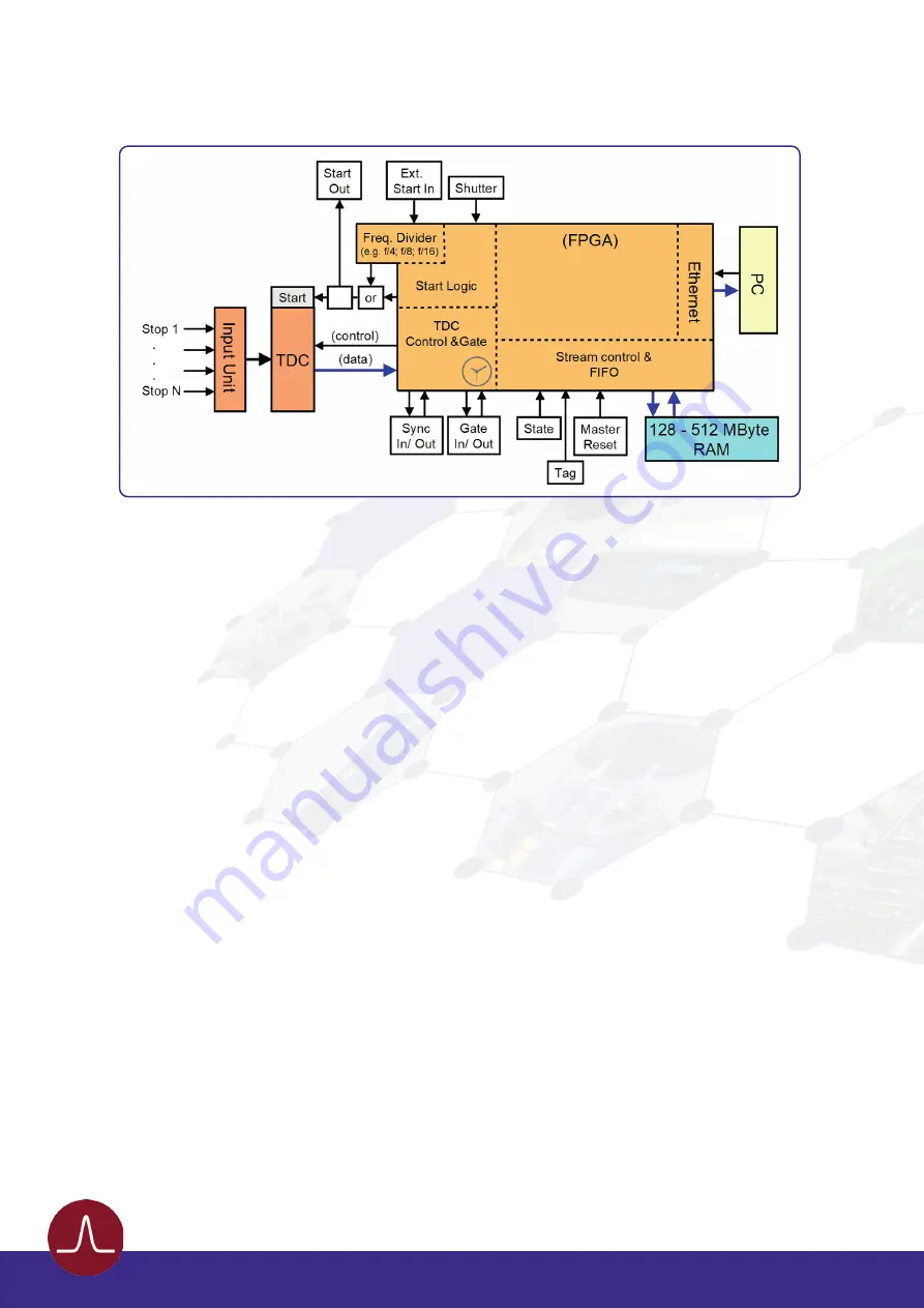
Figure 2b: TDC block diagram (R443, R451, R461).
The stop pulses are distributed via an input unit to the different stop inputs of the TDC, in a specific manner
depending on the specific device layout. The arrival times of the pulses are measured by the TDC with
respect to either an internal reference start signal, provided by the FPGA, or an external start signal. An
internal electronics provides the TDC start signal to an additional BNC socket (“START OUT”) for further
extended measurement use. The measurement dwell times for data from the TDC are settled within the
FPGA by a quartz stabilized time gate in an interval from 1ms to 1193h. The synchronization pulse for the
external acquisition start (“SYNC IN”) is transferred directly into the FPGA that controls the acquisition
process. The FPGA also sends out a synchronization pulse for marking the end of an acquisition (“SYNC
OUT”). Additional counter inputs (e.g. “TAG”) and other inputs for advanced measurements are available.
The TDC data streaming is performed with a specific pre-conditioning of the DLD data, which includes
channel pairing, pair result arithmetic and many more. Communication to and from the PC is achieved
via a USB or Ethernet interface. Data streaming via the interface is provided without losses using a large
memory buffer within the device.
Time-to-Digital-Converter Octa Channel TDC Manual | Surface Concept GmbH


