background image

2-3

Safety Information and Technical Specifications

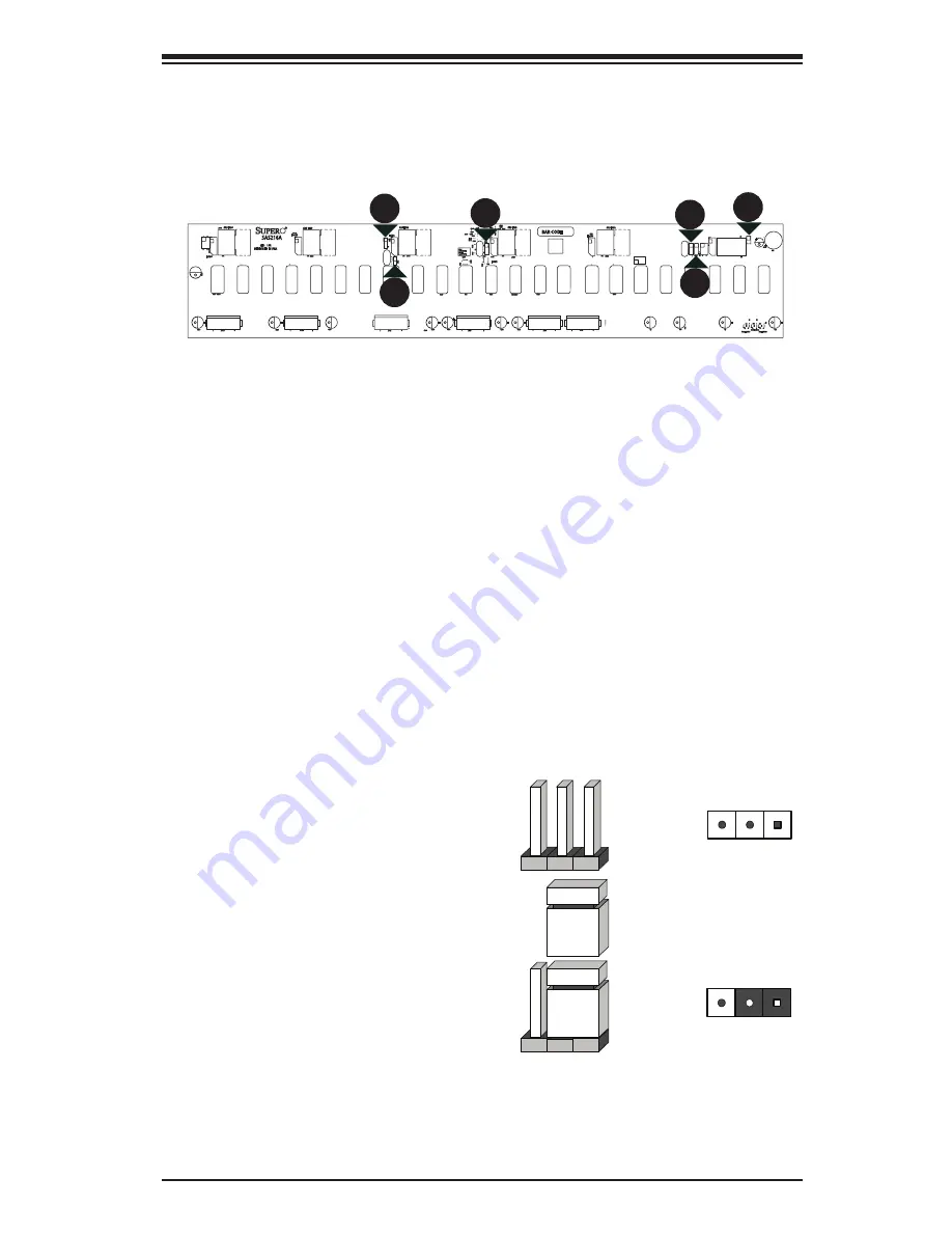
Chip Reset JP36 1-2 Reset, 2-3 No Reset (Not populated)
Chip Reset JP35 1-2 Reset, 2-3 No Reset (Not populated)
Buzzer Reset JP18
JP84 1-2 SGPIO, 2-3 I

2

C

JP80 I

2

C Addr - On C0, Off C2 (Not populated)

JP50 Chip Reset 1-2 Reset, 2-3 No Reset (Not populated)

15.
16.
17.
18.
19.
20.

2-3  Front Jumper Locations and Pin Definitions

Explanation of Jumpers

To modify the operation of the backplane, 
jumpers  can  be  used  to  choose  between 
optional  settings.  Jumpers  create  shorts 
between  two  pins  to  change  the  function 
of  the  connector.  Pin  1  is  identified  with 
a square solder pad on the printed circuit 
board. Note: On two pin jumpers, "Closed" 
means the jumper is on and "Open" means 
the jumper is off the pins. 

Connector

Pins

Jumper

Setting

3

2

1

3

2

1

C6

C5

C47

C44

C420

C415

C327

C323

C253

C239

C201

C197

Y2

BZ1

C157

C224

C24

C247

C295

C298

C383

C399

C139

C153

C220

C244

C246

C249

C250

C280

C294

C297

C212

C213

D4

D9

D3

JP80

R7

R8

R608

R585

R365

R268

R281

R283

R431

R6

R267

R280

R282

R430

R273

R286

R287

R432

JP84

JP36

JP96

JP95

JP52

JP117

JP116

JP48

JP46

JP110

JP109

JP10

JP13

U91

U88

JSM6

JSM2

JSM3

JSM4

JSM5

U53

U30

+

+

+

+

+

+

+

+

B1

A1

BAR CODE

DESIGNED IN USA

SAS216A

REV: 1.02

+

+

A

C

A

C

A

C

1

3

1

3

1

3

1

3

1

4

1

4

1

4

1

4

1

4

1

4

2

5

6

1

2

5

6

SAS IN#2

SAS IN#3

SAS IN#4

SAS IN#5

SAS IN#6

I2C#6

I2C#5

I2C#4

JP36

9072#2 RST
1-2:RST

2-3:NO RST

I2C#3

I2C#2

D9:ALARM#3

D4:ALARM#2

D3:ALARM#1

20

18

19

16

17

15

Summary of Contents for SAS-216A

Page 1: ... R268 R281 R283 R431 R6 R267 R280 R282 R430 R273 R286 R287 R432 JP84 JP36 JP96 JP95 JP52 JP117 JP116 JP48 JP46 JP110 JP109 JP10 JP13 U91 U88 JSM6 JSM2 JSM3 JSM4 JSM5 U53 U30 B1 A1 BAR CODE DESIGNED IN USA SAS216A REV 1 02 A C A C A C 1 3 1 3 1 3 1 3 1 4 1 4 1 4 1 4 1 4 1 4 2 5 6 1 2 5 6 SAS IN 2 SAS IN 3 SAS IN 4 SAS IN 5 SAS IN 6 I2C 6 I2C 5 I2C 4 JP36 9072 2 RST 1 2 RST 2 3 NO RST I2C 3 I2C 2 D9...

Page 2: ...exclusive venue for the resolution of any such disputes Super Micro s total liability for all claims will not exceed the price paid for the hardware product FCC Statement This equipment has been tested and found to comply with the limits for a Class A digital device pursuant to Part 15 of the FCC Rules These limits are designed to provide reasonable protection against harmful interference when the...

Page 3: ...A Note to Users 1 2 Chapter 2 Jumper Settings and Pin Definitions 2 1 Front Connectors and Jumpers 2 1 Front Connectors 2 1 2 2 Front Connector and Pin Definitions 2 2 2 3 Front Jumper Locations and Pin Definitions 2 3 Explanation of Jumpers 2 3 I2 C and SGPIO Modes and Jumper Settings 2 4 Front LED Indicators 2 5 4 4 Rear Components Connectors and LED Indicators 2 6 ...

Page 4: ... Address Super Micro Computer B V Het Sterrenbeeld 28 5215 ML s Hertogenbosch The Netherlands Tel 31 0 73 6400390 Fax 31 0 73 6416525 Email sales supermicro nl General Information support supermicro nl Technical Support rma supermicro nl Customer Support Asia Pacific Address Super Micro Computer Inc 4F No 232 1 Liancheng Rd Chung Ho 235 Taipei County Taiwan R O C Tel 886 2 8226 3990 Fax 886 2 8226 ...

Page 5: ...e mailed when service is complete For faster service RMA authorizations may be requested online http www supermicro com support rma Whenever possible repack the backplane in the original Supermicro box using the original packaging materials If these are no longer available be sure to pack the backplane in an anti static bag and inside the box Make sure that there is enough packaging material surro...

Page 6: ...t static discharge Touch a grounded metal object before removing a component from the antistatic bag Handle the backplane by its edges only do not touch its components peripheral chips memory modules or gold contacts When handling chips or modules avoid touching their pins Put the card and peripherals back into their antistatic bags when not in use 1 2 General Safety Guidelines Always disconnect p...

Page 7: ...A Note to Users All images and layouts shown in this user s guide are based upon the latest PCB Revision available at the time of publishing The card you have received may or may not look exactly the same as the graphics shown in this manual ...

Page 8: ...1 12 13 14 C6 C5 C47 C44 C420 C415 C327 C323 C253 C239 C201 C197 Y2 BZ1 C157 C224 C24 C247 C295 C298 C383 C399 C139 C153 C220 C244 C246 C249 C250 C280 C294 C297 C212 C213 D4 D9 D3 JP80 R7 R8 R608 R585 R365 R268 R281 R283 R431 R6 R267 R280 R282 R430 R273 R286 R287 R432 JP84 JP36 JP96 JP95 JP52 JP117 JP116 JP48 JP46 JP110 JP109 JP10 JP13 U91 U88 JSM6 JSM2 JSM3 JSM4 JSM5 U53 U30 B1 A1 BAR CODE DESIGN...

Page 9: ...n Power 4 Pin Connector JP10 JP13 JP46 JP48 JP109 and JP110 Pin Definition 1 12V 2 and 3 Ground 4 5V 8 Backplane Main Power Connectors The 4 pin connectors designated JP10 JP13 JP46 JP48 JP109 and JP110 provide power to the backplane See the table on the right for pin definitions 9 14 SAS IN Ports Sideband included The SAS ports are used to connect the SAS drive cables The six SAS IN ports are des i...

Page 10: ...the printed circuit board Note On two pin jumpers Closed means the jumper is on and Open means the jumper is off the pins Connector Pins Jumper Setting 3 2 1 3 2 1 C6 C5 C47 C44 C420 C415 C327 C323 C253 C239 C201 C197 Y2 BZ1 C157 C224 C24 C247 C295 C298 C383 C399 C139 C153 C220 C244 C246 C249 C250 C280 C294 C297 C212 C213 D4 D9 D3 JP80 R7 R8 R608 R585 R365 R268 R281 R283 R431 R6 R267 R280 R282 R43...

Page 11: ...he default mode and can be used without making changes to your jumper The following information details which jumper must be configured to use SGPIO mode or restore your backplane to I2 C mode SGPIO Setting Default Jumper Jumper Setting Note JP84 1 2 SGPIO Mode Setting I2 C Setting Jumper Jumper Setting Note JP84 2 3 I2C Setting ...

Page 12: ...P116 JP48 JP46 JP110 JP109 JP10 JP13 U91 U88 JSM6 JSM2 JSM3 JSM4 JSM5 U53 U30 B1 A1 BAR CODE DESIGNED IN USA SAS216A REV 1 02 A C A C A C 1 3 1 3 1 3 1 3 1 4 1 4 1 4 1 4 1 4 1 4 2 5 6 1 2 5 6 SAS IN 2 SAS IN 3 SAS IN 4 SAS IN 5 SAS IN 6 I2C 6 I2C 5 I2C 4 JP36 9072 2 RST 1 2 RST 2 3 NO RST I2C 3 I2C 2 D9 ALARM 3 D4 ALARM 2 D3 ALARM 1 Front Panel LEDs LED STATE SPECIFICATION D3 On Alarm 1 D4 On Alar...

Page 13: ...7 8 7 9 22 21 33 27 8 7 9 22 21 33 27 8 7 9 22 21 33 27 8 7 9 SAS 17 SAS 0 SAS 1 SAS 2 SAS 3 SAS 4 SAS 6 SAS 7 SAS 8 SAS 9 SAS 10 SAS 11 SAS 12 SAS 13 SAS 14 SAS 15 SAS 16 SAS 18 SAS 19 SAS 20 SAS 21 SAS 22 SAS 23 FAIL 0 ACT 0 FAIL 1 ACT 1 FAIL 2 ACT 2 FAIL 3 ACT 3 FAIL 4 ACT 4 FAIL 5 ACT 5 FAIL 6 ACT 6 FAIL 7 ACT 7 FAIL 8 ACT 8 FAIL 9 ACT 9 FALI 10 ACT 10 FAIL 11 ACT 11 FAIL 12 ACT 12 FAIL 13 ACT...

Page 14: ...23 SAS 2 D40 D37 SAS 3 D102 D107 SAS 4 D13 D6 SAS 5 D24 D29 SAS 6 D41 D38 SAS 7 D104 D108 SAS 8 D14 D7 SAS 9 D25 D30 SAS 10 D42 D39 SAS 11 D106 D109 SAS 12 D15 D8 SAS 13 D26 D31 SAS 14 D87 D88 SAS 15 D111 D110 SAS 16 D18 D19 SAS 17 D27 D32 SAS 18 D100 D103 SAS 19 D118 D119 SAS 20 D21 D20 SAS 21 D28 D33 SAS 22 D101 D105 SAS 23 D120 D121 ...

Page 15: ...orm be reasonably expected to result in significant injury or loss of life or catastrophic property damage Accordingly Supermicro disclaims any and all liability and should buyer use or sell such products for use in such ultra hazardous applications it does so entirely at its own risk Furthermore buyer agrees to fully indemnify defend and hold Supermicro harmless for and against any and all claims ...

Reviews: