13
Chapter 1: Introduction
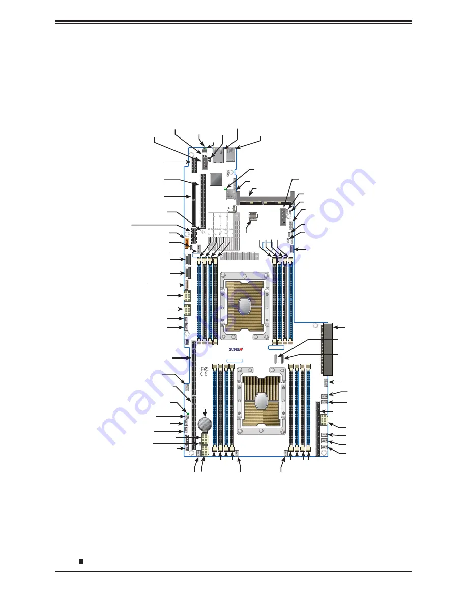
Figure 1-5. Motherboard Layout
1.5 Motherboard Layout
Below is a layout of the X11DPG-SN with jumper, connector and LED locations shown. See
the table on the following page for descriptions. For detailed descriptions, pinout information
and jumper settings, refer to Chapter 4.
DESIGNED IN USA
BIOS
LICENSE
BAR CODE
MAC CODE
X11DPG-SN
REV:1.00
IPMI CODE
DESIGNED IN USA
REV:1.00
X11DPG-SN
JBR1
UID
LE1
JUIDB1
JWD1
COM
JCOM1
SXB1A
CPU2 PCIE 3.0 X8
SXB1B CPU1 PCIE 3.0 X16
SXB1C
JPCIE1_1
JPCIE5
JPCIE1_2
JPCIE1_3
JNVME1
JNVME2
P2_NVME0
P2_NVME1
FAN H
FAN F
FAN E
FAN G
CPU2 PCIE3.0 X16
JPCIE4
JPW7
FAN 1
BIOS
JPW2
JPME1
JPME2
JRK1
RAID KEY-1
JPG1
JD1
JTPM1
TPM/PORT80
JPW1
JVGA
VGA
P1
DIMM A2
P2 DIMM D2
P1 DIMM F1
P2 DIMM C1
P1 DIMM C1
P2 DIMM F1
FAN 4
FAN 3
FAN 2
P1 DIMM D2
P2
DIMM A2
P1
DIMM A1
P2 DIMM D1
P1 DIMM E1
P2 DIMM B1
P1 DIMM B1
P2 DIMM E1
JPW3
P1 DIMM D1
P2
DIMM A1
I-SATA0-3
I-SATA4-7
S-SATA1
JPW5
JPW6
FAN D
FAN C
S-SGPIO
CPU2 PCIE 3.0 X16
CPU1 PCIE 3.0 X16
JPCIE2
JPCIE3
LEDPWR
LE2
JF2
FAN B
JPW4
FAN A
JF1
BT1
JL1
JS1
JS2
LEDBMC
LEDM1
JSDCARD1
JSIOM
S-SATA0
JBT1
CMOS CLEAR
JSTBY1
JIPMB1
JUSB
USB0/1(3.0)
IPMI_LAN
Notes:
•
Jumpers/LED indicators not indicated are used for testing only.
•
" " indicates the location of pin 1.


