background image

Ele
c

tric

al sch

emat

ics

UM24

03

6

2/7

8

U

M2
403
 Re
v 1

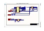
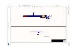
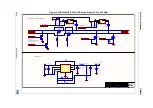
Figure 43. STM32G081B-EVAL legacy peripheral daughterboard temperature sensor and LDR

5

5

TemSensor_LDR

Title:

Size:

Reference:
Sheet:

of

A4

Revision:

Project:

STM32G081B-EVAL  Legacy  peripheral  daughter  board

MB1351

A 01

17-MAY-17

Variant  name  is  not  interpreted  until  output

Date:

-

Variant:

SDA

1

SCL

2

OS/INT

3

GND

4

A2

5

A1

6

A0

7

VDD

8

U3

STLM75M2F

+5V

C7
100nF

R23
10K

VDD

I2C1_SCL_5V

I2C1_SDA_5V

Temperature  sensor

TempSensor_INT

PB7
PB6
PB5

R19
10K

+5V

Address:100100(A0)

LDR_OUT

R2

8.2K

PA1

R1
VT9ON1

Photo  resistor

VDD_ANA

SB7

Summary of Contents for STM32G081B-EVAL

Page 1: ...ll peripherals USB Type C connector with USB PD motor control connector RS232 RS485 Audio DAC microphone ADC TFT LCD IrDA IR LED IR receiver LDR microSD card CEC on two HDMI connectors smartcard slot RF E2PROM and temperature sensor etc and to develop applications An ST LINK V2 1 is integrated on the board as embedded in circuit debugger and programmer for the STM32 MCU The daughterboard and exten...

Page 2: ... 1 1 Drivers 15 8 1 2 ST LINK V2 1 firmware upgrade 15 8 2 Power supply 16 8 3 Clock references 20 8 4 Reset source 20 8 5 Boot Option 21 8 6 Peripherals on mother board 21 8 6 1 Audio 21 8 6 2 RS232 and RS485 22 8 6 3 microSD card 23 8 6 4 Analog Input 23 8 6 5 External I2C Connector 23 8 6 6 Motor Control 24 8 6 7 Display and Input devices 24 8 7 Peripherals on legacy peripheral daughterboard 25...

Page 3: ...7 35 9 1 6 microSD connector CN8 35 9 1 7 Extension connector CN9 and CN10 35 9 1 8 RS232 and RS485 connector CN11 37 9 1 9 Standard SWD connector CN12 38 9 1 10 High density SWD connector CN13 39 9 1 11 TFT LCD connector CN14 39 9 1 12 Audio jack CN15 39 9 1 13 5 V Power connector CN16 39 9 1 14 Analog input connector CN17 40 9 2 Connectors on legacy peripheral daughterboard 40 9 2 1 HDMI sink co...

Page 4: ... STM32G081B EVAL IO Assignment 72 Appendix C Federal Communications Commission FCC and Industry Canada IC Compliance Statements 75 C 1 FCC Compliance Statement 75 C 1 1 Part 15 19 75 C 1 2 Part 15 105 75 C 1 3 Part 15 21 75 C 2 IC Compliance Statement 75 C 2 1 Compliance Statement 75 C 3 Déclaration de conformité 75 Appendix D Mechanical dimensions 76 Revision history 77 ...

Page 5: ...umpers 30 Table 19 Motor control connector CN1 31 Table 20 RF E2PROM connector CN2 32 Table 21 Daughterboard connector CN4 33 Table 22 Daughterboard connector CN5 33 Table 23 USB Micro B connector CN6 34 Table 24 microSD connector CN9 35 Table 25 Extension connector CN9 36 Table 26 Extension connector CN10 36 Table 27 RS232 RS485 connector CN11 37 Table 28 Standard SWD debugging connector CN12 38 ...

Page 6: ...yPort source connector CN2 front view 43 Figure 24 19 V Power connector CN3 front view 43 Figure 25 USB3 1 Gen1 Type B connector CN4 front view 44 Figure 26 USB Type C connector PORT2 CN5 front view 44 Figure 27 DisplayPort sink connector CN6 front view 45 Figure 28 USB Type C connector PORT1 CN7 front view 46 Figure 29 STM32G081B EVAL mother board top 48 Figure 30 STM32G081B EVAL MCU 49 Figure 31...

Page 7: ...M32G081B EVAL UCPD daughterboard Type C sink con 68 Figure 50 STM32G081B EVAL UCPD daughterboard USB PD 69 Figure 51 STM32G081B EVAL UCPD daughterboard power 70 Figure 52 STM32G081B EVAL UCPD daughterboard source power 71 Figure 53 Mechanical dimensions 76 ...

Page 8: ...ncluding analog microphone input microSD card Extension I2 C connector Motor control connector Board extension connectors Daughterboard connectors for legacy peripheral daughterboard or USB Type C and Power Delivery daughterboard Extension connectors for daughterboard or wire wrap board Flexible power supply options 5 V power jack ST LINK V2 1 USB connector Daughterboard On board ST LINK V2 1 debu...

Page 9: ...ard slot USB Type C and Power Delivery daughterboard Multiplexer for USB3 1 Gen1 DisplayPort input and Type C port1 output Multiplexer for Type C port2 input and DisplayPort output USB2 0 VCONN on Type C port1 USB PD on Type C port1 Board connectors Type C port1 DRP Dual Role Port Type C port2 sink DisplayPort input DisplayPort output USB 3 1 Gen1 Type B receptacle USB2 0 Type A receptacle 19 V po...

Page 10: ...e information in the STM32 datasheet at www st com next to the evaluation tool ordering part number that is stuck or silkscreen printed on the board 3 System requirements Windows OS 7 8 and 10 Linux 64 bit or macOS a USB Type A to Micro B cable 4 Development toolchains Keil MDK ARM b IAR EWARM b GCC based IDEs 5 Demonstration software The demonstration software included in the STM32Cube MCU Packag...

Page 11: ... and that no components are unplugged or lost When the board is extracted from its plastic bag check that no component remains in the bag The main component to verify is microSD card which may have been ejected from the connector CN8 right side of the board Caution There is an explosion risk if the battery is replaced by an incorrect one Make sure to dispose of used batteries according to the inst...

Page 12: ... Figure 4 help users to locate these features on the Evaluation board Figure 3 Hardware block diagram 06Y 9 670 5 7 3 2 5B287 86 7 0 B 63 86 57 6 86 57 0RWKHU ERDUG HJDF SHULSKHUDO GDXJKWHUERDUG 86 GDXJKWHUERDUG 3 2 NH WDPSHU EXWWRQ V PRWRU FRQWURO FRQQHFWRU SRWHQWLRPHWHU YROWDJH WUDQVODWRU 03 B 1S PLFUR6 FDUG GRW PDWUL 56 WUDQVFHLYHU 56 WUDQVFHLYHU FRQQHFWRU YROWDJH WUDQVODWRU HPEHGGHG 67 1 9 86 ...

Page 13: ...RQWURO VLJQDO VHOHFWLRQ 1 PRWRU FRQWURO FRQQHFWRU 1 1 GDXJKWHUERDUG FRQQHFWRUV 1 PLFUR6 FDUG 1 6 FRQQHFWRU 1 6 FRQQHFWRU 1 DXGLR MDFN 1 7 7 59 SRWHQWLRPHWHU MR VWLFN WDPSHU EXWWRQ UHVHW EXWWRQ 59 9 DGMXVWPHQW XVHU V 1 SRZHU MDFN ORZ YROWDJH DODUP 1 86 57 1 1 H WHQVLRQ KHDGHU 8 670 5 7 1 67 1 9 86 1 H WHQVLRQ FRQQHFWRU 67 1 9 20 ...

Page 14: ...Legacy peripheral daughterboard Figure 6 USB Type C and Power Delivery daughterboard 06Y 9 1 0 VRXUFH 1 0 VLQN 5 5 1 VPDUWFDUG 5 5 UHFHLYHU 06Y 9 1 7 SH 53 GXDO UROH SRUW 1 LVSOD 3RUW LQSXW 1 86 FRQQHFWRU 1 H WHQVLRQ SRZHU LQSXW 1 LVSOD 3RUW RXWSXW 1 86 7 SH 1 7 SH VLQN ...

Page 15: ...s is connected to CN12 or CN13 External SWD connector 8 1 1 Drivers The ST LINK V2 1 requires a dedicated USB driver which can be found on www st com for Windows PC 7 8 or 10 In case the STM32G081B EVAL Evaluation board is connected to the PC before the driver is installed some STM32G081B EVAL interfaces may be declared as Unknown in the PC device manager In this case the user must install the dri...

Page 16: ...rd This power switch features also a current limitation to protect the PC in case of short circuit on the board If overcurrent more than 500 mA happens on the board the LED LD5 lights up 5 V DC power from CN6 directly the USB Micro B connector of STLINK V2 1 USB 5 V power source on silkscreen of JP17 U5V 5 V DC power from CN5 or CN9 the extension connector for daughterboard power source D5V on sil...

Page 17: ...he enumeration fails Therefore the STM32 part including the extension board is not powered As a consequence the red LED LD7 remains turned OFF In this case it is mandatory to use an external power supply to supply extra power E5V from PSU or D5V can be used as external power supply in case current consumption of the STM32G081B EVAL board exceeds the allowed current on USB In this condition it is s...

Page 18: ...s not powered LED LD7 remains OFF In case the STM32G081B EVAL board is powered by an USB charger through CN6 there is no USB enumeration needed User can set JP17 to U5V to allow the board to be powered anyway from CN6 The power source is selected by setting the related jumpers JP17 JP15 and JP16 as described in table 2 Table 2 Power source related Jumpers Jumper Description JP17 JP17 is used to se...

Page 19: ...cteristics of some peripheral components Components might work incorrectly when the power level is lower than the limitation JP15 The Vbat pin of STM32G081RBT6 is connected to VDD when JP15 is set as shown on the right default setting The Vbat pin of STM32G081RBT6 is connected to 3V battery when JP15 is set as shown on the right JP16 The VDD pin of STM32G081RBT6 is connected to 3 3V when JP16 is s...

Page 20: ... related solder bridges Jumper Description SB18 PC14 is connected to 32KHz crystal when SB18 is open default setting PC14 is connected to extension connector CN9 when SB18 is closed In such case R43 must be removed to avoid disturbance due to the 32Khz quartz SB19 PC15 is connected to 32KHz crystal when SB19 is open default setting PC15 is connected to extension connector CN9 when SB19 is closed I...

Page 21: ... to ADC input of STM32G081RBT6 through a microphone amplifier Audio amplifier can be enabled or disabled by setting of JP18 and mono stereo playback can be chosen by setting of JP6 refer to Table 8 for detail Table 6 Boot related jumper Jumper configuration Bit25 in USER OPTION BYTES Boot from CN10 pin 19 and pin 17 closed by jumper X STM32G081B EVAL boot from User Flash default setting CN10 pin 1...

Page 22: ...ker amplifier U17 is enabled when JP18 is closed default setting Speaker amplifier U17 is disabled when JP18 is open JP19 PA4 is connected to VIN1 of Audio amplifier when JP19 is closed default setting PA4 is disconnected to VIN1 of Audio amplifier when JP19 is open JP6 Mono playback is enabled when JP6 is set as shown on the right default setting Stereo playback is enabled when JP6 is set as show...

Page 23: ... CN2 connector and accessed by the microcontroller through the I2C1 bus it shares same I2C1 bus with Temperature sensor U3 and DDC on HDMI_Source connector CN3 on legacy peripheral daughterboard The pull up voltage level of I2C1 bus is automatically decided by the daughterboard the legacy peripheral daughterboard or the UCPD daughterboard on CN4 and CN5 If there is JP8 PC5 is connected as RX signa...

Page 24: ...rol application Close JP1 JP2 and JP3 Open JP4 and JP6 Open pin2 3 of JP8 and JP10 8 6 7 Display and Input devices The 2 4 color TFT LCD connected to SPI1 port of STM32G081RBT6 and 4 general purpose color LED s LD 1 2 3 4 are available as display device The 4 direction joystick B3 with selection key which connected to PA0 and supports wakeup feature Tamper button B2 are also available as input dev...

Page 25: ... for AD conversion 8 7 2 Temperature sensor A temperature sensor STLM75M2F is connected to the I2C1 bus of the STM32G081RBT6 and shares same I2C1 bus with EXT I2C connector on mother board and DDC on HDMI_Source connector CN3 on legacy board I2C address of temperature sensor is 0b100100 A0 A0 can be 0 or 1 depends on the setting of SB7 Note The temperature result measured from STLM75M2F would be a...

Page 26: ...nnector HPD controlled by IO PD3 CEC connected to PB10 through transistor T4 HDMI 5V powered by power switch U1 The signals TDMS D 0 2 TDMS_CLK TDMS D 0 2 TDMS_CLK on these two HDMI connectors are connected together The CEC injector mode can be enabled by some PCB reworks for debugging purpose only Remove resistors R3 R4 R7 R9 R10 R15 and R22 Close solder bridges SB3 SB4 SB5 and SB6 Note The I O P...

Page 27: ... 8 1 USB Type C receptacles Two USB Type C certified receptacles CN7 and CN5 are present on the UCPD daughterboard representing respectively the PORT 1 and PORT 2 PORT 1 can be used as DRP Dual Role Port which is eligible to supply another platform plugged by a USB Type C cable when they are configured as Provider or otherwise to be supplied in case of Consumer configuration PORT 2 can only be use...

Page 28: ...P5 is used to select D5V resources in Table 15 8 8 3 VBUS management and discharge mechanism Type C port1 CN7 can be used as DRP Dual Role Port its VBUS can be managed for supplying other platforms as Provider or to be supplied as Consumer Two MOSFETs T6 and T7 are set in back to back configuration to protect and isolate the VBUS supplying path on both directions If the CN7 acts as Provider the VB...

Page 29: ... VBUS 8 8 5 CC management Dead battery VCONN output and fast role swap functions are supported on CC signal of Type C PORT 1 1 Dead battery enable Dead battery function is supported by OVP chip U17 and U16 And this function also Table 16 VBUS Power Delivery profiles CN7 role Solder bridges setting Power level Source control signal Voltage control signal Provider SB2 SB3 SB23 SB26 ON SB13 SB14 SB15...

Page 30: ...n of the PD4 or PB9 and the load switches STMPS2161 U10 and U14 3 Fast role swap Type C PORT 1 can be configure to action fast role swap managed by STM32G081RBT6 through PA2 CC1 and PB0 CC2 Table 18 Dead battery related jumpers Jumper Description JP1 Embed dead battery function is enable when JP1 is set as shown on the right default setting Embed dead battery function is disable when JP1 is set as...

Page 31: ...ber of CN1 Pin of STM32G081RBT6 Description EmergencySTOP PB12 1 2 GND PWM UH PA8 3 4 GND PWM UL PD2 5 6 GND PWM VH PA9 7 8 GND PWM VL PD3 9 10 GND PWM WH PA10 11 12 GND PWM WL PD4 13 14 PA1 BUS VOLTAGE PHASE A CURRENT PA2 15 16 GND PHASE B CURRENT PA6 17 18 GND PHASE C CURRENT PB10 19 20 GND NTC BYPASS RELAY PB9 21 22 GND DISSIPATIVE BRAKE PWM PB15 23 24 GND 5V power 25 26 PA3 Heatsink temperatur...

Page 32: ...CN5 can be used by a daughterboard after disconnecting it from the corresponding function block on STM32G081B EVAL Evaluation board Please refer to Table 21 and Table 22 for detail Encoder A PC6 31 32 GND Encoder B PB5 33 34 PB0 Encoder Index Table 19 Motor control connector CN1 continued Description Pin of STM32G081RBT6 Pin number of CN1 Pin number of CN1 Pin of STM32G081RBT6 Description Table 20...

Page 33: ...ntC HDMI_CEC ISENSE 1 12 PA3 MC_heatsinkTemp Smartcard 1V8 VSENSE 2 Keep JP2 open 13 PB12 MC_EmergencyST OP Smartcard OFF ISENSE 2 Keep JP3 open 14 3V3 15 PB11 Daughterboard detection Daughterboard detection Daughterboard detection USB PD output VSENSE 16 VDD_ANA 17 I2C_PU I2C pull up power of CN2 18 VDD Table 22 Daughterboard connector CN5 Pin Signal Mother board Function Legacy daughterboard Fun...

Page 34: ... 11 PB5 MC_ENB Temp Sensor INT Display port HPD_IN 12 PC1 MC_PFCsync1 V_CTL1 13 PD0 MC_PFCsync2 PORT2_CC1 14 PD2 MC_UL HDMI_ HPD_SINK PORT2_CC2 15 PD3 MC_VL HDMI_ HPD_SOURCE SOURCE_EN 16 D5V 17 EXT I2C PWR Power of CN2 5V VDD 18 VDD Table 22 Daughterboard connector CN5 continued Pin Signal Mother board Function Legacy daughterboard Function CN4 UCPD daughterboard Function CN8 How to disconnect wit...

Page 35: ...rd or standard wrapping board to STM32G081B EVAL Evaluation board The standard width between CN9 pin1 and CN10 pin1 is 2700mils 68 58mm The standard was implemented on the majority of Evaluation boards Each pin on CN9 and CN10 can be used by a daughterboard after disconnecting it from the corresponding function block on STM32G081B EVAL Evaluation board Please refer to Table 25 and Table 26 for det...

Page 36: ... SB42 2 PD9 LED4 Close SB10 Open SB13 SB33 4 PA11 USART_1_CTS Open SB28 6 PC8 GPIO_JOY_LEFT Open SB39 8 PD1 GPIO_SD_CS Open SB9 10 GND 12 PC5 USART_1_RX Open JP8 pin1 2 14 PB4 LCD SD1_MISO Open SB12 16 PC11 VCP_USART_3_RX Open JP7 18 PC15 OSC32_OUT Remove R44 Close SB19 20 D5V 22 3V3 Table 26 Extension connector CN10 Pin Description Alternative Function How to disconnect with function block on STM...

Page 37: ...10 GND 12 PC0 GPIO_EXT_RST Remove R12 Keep CN2 disconnected 14 PC3 GPIO_JOY_DOWN Open SB37 16 PC12 GPIO_LCD SD_MOSI_DIR Open SB26 18 PF2 NRST RESET Open SB23 20 PF3 VBAT VBAT Open JP15 22 PF4 VREF VREF Open SB17 SB22 Table 26 Extension connector CN10 continued Pin Description Alternative Function How to disconnect with function block on STM32G081B EVAL board Table 27 RS232 RS485 connector CN11 Pin...

Page 38: ...27 RS232 RS485 connector CN11 continued Pin number Description Pin number Description Table 28 Standard SWD debugging connector CN12 Pin number Description Pin number Description 1 VDD 2 VDD 3 NC 4 GND 5 NC 6 GND 7 SWDAT PA13 8 GND 9 SWCLK PA14 10 GND 11 10K pull down 12 GND 13 NC 14 GND 15 RESET 16 GND 17 10K pull down 18 GND 19 10K pull down 20 GND D ϯϬϳϮϮsϮ ...

Page 39: ...ected to audio DAC and ADC is available on STM32G081B EVAL board 9 1 13 5 V Power connector CN16 STM32G081B EVAL Evaluation mother board can be powered from a DC 5V power supply via the external power supply jack CN16 shown in Figure 17 The central pin of CN16 must be positive Figure 17 Power supply connector CN16 front view Table 29 High density SWD debugging connector CN13 Pin number Description...

Page 40: ...DMI sink connector CN1 front view Table 30 Analog input output connector CN17 Pin number Description Pin number Description 1 Analog input output PB2 2 GND 06Y 9 Table 31 HDMI sink connector CN1 Pin number Description Pin number Description 1 3 4 6 7 9 10 12 TMDS differential signal pair connected to CN3 16 I2C2_SDA PB14 13 CEC PB10 2 5 8 11 17 GND 14 NC 18 HDMI_5V_Sink 15 I2C2_SCL PB13 19 HPD PD2...

Page 41: ...card connector CN2 Figure 20 Smartcard connector CN2 top view Table 32 Smartcard connector CN2 Pin number Description Pin number Description 1 VCC 5 GND 2 RST 6 NC 3 CLK 7 I O 4 NC 8 NC 17 Card presence detection pin 18 Card presence detection pin 06Y 9 ...

Page 42: ...d to CN4 on mother board Please refer to Section 9 1 3 for detail signal definition of these connectors 9 3 Connectors on UCPD daughterboard 9 3 1 USB Type A connector CN1 Figure 22 USB Type A connector CN1 front view Table 33 HDMI source connector CN3 Pin number Description Pin number Description 1 3 4 6 7 9 10 12 TMDS differential signal pair connected to CN1 16 I2C1_SDA PB7 13 CEC PB10 2 5 8 11...

Page 43: ...C 19 V power supply via the external power supply jack CN3 shown in Figure 24 And it is used for USB PD Figure 24 19 V Power connector CN3 front view Table 35 DisplayPort source connector CN2 Pin number Description Pin number Description 1 LANE0_P 13 CONFIG1 3 LANE0_N 14 CONFIG2 4 LANE1_P 15 AUX_CH_P 6 LANE1_N 17 AUX_CH_N 7 LANE2_P 18 HPD PC6 9 LANE2_N 19 RETURN 10 LANE3_P 20 DP_PWR 12 LANE3_N 2 5...

Page 44: ...B Type C connector PORT2 CN5 front view Table 36 USB3 1 Gen1 Type B connector CN4 Pin number Description Pin number Description 1 VBUS power 5 SSTX 2 D 6 SSTX 3 D 7 GND_DRAIN 4 GND 8 SSRX 9 SSRX Table 37 USB Type C connector PORT2 CN5 Pin number Description Pin number Description A1 GND B1 GND A2 TX1 B2 TX2 A3 TX1 B3 TX2 A4 VBUS B4 VBUS A5 CC1 PD0 B5 CC2 PD2 A6 D B6 D A7 D B7 D ...

Page 45: ...RX2 B11 RX1 A12 GND B12 GND Table 37 USB Type C connector PORT2 CN5 continued Pin number Description Pin number Description Table 38 DisplayPort sink connector CN6 Pin number Description Pin number Description 1 LANE3_N 13 CONFIG1 3 LANE3_P 14 CONFIG2 4 LANE2_N 15 AUX_CH_P 6 LANE2_P 17 AUX_CH_N 7 LANE1_N 18 HPD PB5 9 LANE1_P 19 RETURN 10 LANE0_N 20 DP_PWR 12 LANE0_P 2 5 8 11 16 GND ...

Page 46: ...PD the daughterboard is connected to CN5 on the mother board and CN9 on the UCPD daughterboard is connected to CN4 on the mother board Please refer to Section 9 1 3 for detail signal definition of these connectors Table 39 USB Type C connector PORT1 CN7 Pin number Description Pin number Description A1 GND B1 GND A2 TX1 B2 TX2 A3 TX1 B3 TX2 A4 VBUS B4 VBUS A5 CC1 PA8 B5 CC2 PB15 A6 D B6 D A7 D B7 D...

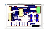
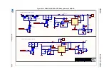
Page 47: ...L legacy peripheral daughterboard on page 59 Figure 41 STM32G081B EVAL legacy peripheral daughterboard HDMI and CEC on page 60 Figure 42 STM32G081B EVAL legacy peripheral daughterboard Smartcard and IR on page 61 Figure 43 STM32G081B EVAL legacy peripheral daughterboard temperature sensor and LDR on page 62 Figure 44 STM32G081B EVAL UCPD daughterboard top on page 63 Figure 45 STM32G081B EVAL UCPD ...

Page 48: ...pherals Peripherals SchDoc RESET LED4 LED3 LED1 LED2 Bootloader_BOOT0 Bootloader_RESET JOY_SEL MC_BusVoltage MC_CurrentA Audio_OUT_L Audio_OUT_R SPI1_SCK Potentiometer SWCLK USART1_TX_BOOT MC_EnA USART1_RX_BOOT Audio_IN SPI1_MOSI_DIR MC_EnB I2C1_SCL I2C1_SDA MC_EnIndex MC_DissipativeBrake MC_EmergencySTOP SDcard_detect MC_PFCsync1 LCD_CS_OD MicroSD_CS_OD JOY_UP JOY_DOWN MC_HeatsinkTemperature MC_C...

Page 49: ...FCsync2 MC_PFCpwm Tamper_key USART1_CTS USART1_RTS USART1_TX USART1_RX EX_RESET_OD JOY_LEFT JOY_RIGHT MC_NTC MC_UH MC_UL MC_WL MC_VH MC_VL MC_WH SPI1_MISO SPI1_MOSI SWDAT R38 0 PF2 NRST 12 PC0 13 PC1 14 PA6 23 PA7 24 PC4 25 PC5 26 PB2 29 PB10 30 PB11 31 PB12 32 PB15 35 PA8 36 PA9 37 PA15 47 PD3 53 PD4 54 PC11 1 PC12 2 PC13 3 PC14 OSC32_IN 4 PC15 OSC32_OUT 5 PF4 VREF 7 VDD_1 8 VSS_1 9 PC2 15 PC3 16...

Page 50: ...ance C55 100nF R79 N A VDD JP13 VDD_ANA 3 2 1 JP16 TP5 VDD VDD_PG 3V3 VDD_ADJ TP10 5V 5V R71 1K 1 2 LD7 green TP11 Ground E5V D5V 7 8 5 6 3 4 1 2 JP17 Header 4X2 EN 1 GND 2 VO 4 ADJ 5 GND 7 VI 6 PG 3 U14 ST1L05BPUR 5V 5V TP7 3V3 C72 4 7uF C67 N A R88 20 5K 1 R87 11 8K 1 C71 10uF ESR 0 2ohm EN 1 GND 2 VO 4 ADJ 5 GND 7 VI 6 PG 3 U16 ST1L05BPUR Power Supply 3 3V Vout 1 22 1 R1 R2 C64 100nF 3V3 R91 N ...

Page 51: ... 0 R61 510 Audio_IN 4 3 1 2 5 U12 TS461CLT C61 10uF C59 4 7uF C60 2 2uF R68 18K R59 82K R70 680 C58 4 7uF PA6 VDD_ANA VDD_ANA VDD_ANA C50 100nF R108 10K JP18 C69 1uF C66 330nF R89 20K Audio_OUT_L C65 N A C80 330nF R95 20K Audio_OUT_R R93 0 C78 N A R90 4 7K C73 1 5nF R94 4 7K C76 1 5nF C68 220uF R86 1K C77 220uF R92 1K C75 1uF Default setting close C74 100nF VDD_ANA VDD_ANA VDD_ANA 2 2V VDD_ANA 2 7...

Page 52: ... SW1 10 CN8 PJS008 2000 SMS064FF or SMS128FF PB8 PD1 RESET VDD R75 4 7K R76 270 R78 10K R63 270 Open drain pin Open drain pin SPI LCD SPI MICRO SD SPI1_MISO_3V3 PB4 SPI1_MOSI PA7 VCCA 1 A1 2 A2 3 GND 4 DIR 5 B2 6 B1 7 VCCB 8 U10 SN74LVC2T45DCUT VDD VDD C40 100nF C42 100nF SPI1_MOSI_3V3 SPI1_MOSI_DIR R56 10K PC12 SPI1_SCK VCCA 1 A1 2 A2 3 GND 4 DIR 5 B2 6 B1 7 VCCB 8 U11 SN74LVC2T45DCUT VDD VDD C43...

Page 53: ...S RELAY 21 DISSIPATIVE BRAKE 23 5V POWER 25 PFC SYNC 27 PFC PWM 29 Encoder A 31 Encoder B 33 GND 2 GND 4 GND 6 GND 8 GND 10 GND 12 BUS VOLTAGE 14 GND 16 GND 18 GND 20 GND 22 GND 24 Heatsink Temperature 26 3 3V Power 28 GND 30 GND 32 Encoder Index 34 CN1 MC_connector MC_EmergencySTOP MC_CurrentA MC_CurrentB MC_CurrentC MC_PFCsync1 MC_PFCsync2 MC_WL MC_VH MC_VL MC_UH MC_UL MC_WH MC_NTC MC_Dissipativ...

Page 54: ... R110 100 Tamper_key PC13 R11247 VDD_ANA C91 100nF VDD C87 100nF C86 100nF C85 100nF C83 100nF C84 100nF R106 100 COMMON 5 Selection 2 DOWN 3 LEFT 1 RIGHT 4 UP 6 GND 7 GND 8 B3 MT 008A JOY_SEL JOY_DOWN JOY_LEFT JOY_RIGHT JOY_UP Joystick PC2 PC7 PC8 PC3 PA0 Input pins with pull down VDD 3V3 R99 1K 1 R97 4 53K 1 3V3 3V3 6 5 7 U19B TS3702IPT 2 3 1 4 8 U19A TS3702IPT 1 2 LD8 Orange VDD 2 7V R105 0 R98...

Page 55: ...OUT 9 T2OUT 10 T3OUT 11 T3IN 12 T2IN 13 T1IN 14 R5OUT 15 R4OUT 16 R3OUT 17 R2OUT 18 R1OUT 19 R2OUTB 20 R1OUTB 21 nSHDN 22 nEN 23 C1 24 GND 25 VCC 26 V 27 C1 28 U13 ST3241EBPR C49 100nF C45 100nF C52 100nF C48 100nF C44 100nF 3V3 3V3 RXD RTS TXD CTS DSR USART1_CTS_3V3 PA11 RO 1 RE 2 DE 3 DI 4 GND 5 A 6 B 7 Vcc 8 U15 ST3485EBDR 3V3 PA10 3 2 1 JP10 3 2 1 JP8 USART1_RX_BOOT_3V3 PC5 USART1_RTS_3V3 USAR...

Page 56: ...l IR_IN I2C2_SCL I2C2_SDA HDMI_CEC LDR_OUT SMART_RST RESET Mother board SMART_OFF SMART_1V8 I2C1_SCL I2C1_SDA R11 820 R26 10K RESET D5V VDD SB20 SB21 3V3 R47 820 SB18 SB19 Daugher board connectors Extension connectors VDD_ANA R41 820 1 2 3 4 5 6 7 8 9 10 11 12 13 14 15 16 17 18 CN4 Header 18X1 R39 10K BOOT0 1 2 3 4 5 6 7 8 9 10 11 12 13 14 15 16 17 18 19 20 21 22 CN10 Header 11X2 1 2 3 4 5 6 7 8 9...

Page 57: ...VSS_3 47 PA11 32 VDD_3 48 U2 STM32F103CBT6 R16 100K Power Switch to supply 5V from STLINK USB PWR_ENn 3V3_ST_LINK 1 2 3 4 5 CN7 N A C20 100nF C13 100nF C15 100nF C21 100nF 3V3_ST_LINK VUSB_ST_LINK LED_STLINK 2 1 4 3 Red Yellow LD6 HSMF A201 A00J1 R35 100 R36 100 R37 0 3V3_ST_LINK T_JTCK T_NRST T_JTMS TMS SWDIO TCK SWCLK T_SWDIO_IN RESET T_SWDIO_IN STM_JTMS_SWDIO STM_JTCK_SWCLK STM_JTMS_SWDIO STM_J...

Page 58: ...350 B 01 31 AUG 17 Variant name is not interpreted until output Date Variant R49 N A R51 N A R53 N A 1 2 3 4 5 6 7 8 9 10 11 12 13 14 15 16 17 18 19 20 CN12 SWD R55 10K R58 10K R52 10K RESET SWDAT SWCLK High Density SWD connector Standard SWD connector KEY PA13 PA14 R48 22 R50 22 R54 22 1 2 3 4 5 6 7 8 9 10 CN13 FTSH 105 01 L DV VDD VDD VDD 1 3 2 4 5 U9 ESDALC6V1W5 VDD ...

Page 59: ..._SmartCard_IR SmartCard_IR SchDoc I2C1_SCL_5V I2C1_SDA_5V TempSensor_INT LDR_OUT U_TemSensor_LDR TemSensor_LDR SCHDOC SmartCard_3 5V SmartCard_CLK SmartCard_IO SmartCard_CMDVCC SmartCard_1V8 SmartCard_RST SmartCard_OFF IR_IN IR_OUT I2C1_SCL_5V I2C1_SDA_5V TempSensor_INT LDR_OUT HDMI_HPD_Source_5V HDMI_HPD_SINK HDMI_CEC_3V3 I2C1_SCL_5V I2C1_SDA_5V I2C2_SCL_5V I2C2_SDA_5V SMART_CK IR_OUT SMART_TX IR...

Page 60: ...A_5V I2C2_SCL_5V R9 47K R10 47K 3V3 R18 27K HDMI_CEC_3V3 5V C2 4 7uF GND 2 IN 5 EN 4 OUT 1 FAULT 3 U1 STMPS2141STR 54 HDMI_5V_Source R22 1M HDMI_HPD_Source_5V I2C1_SCL_5V I2C1_SDA_5V R4 1 8K R3 1 8K 5V R15 0 5V PD2 PB13 PB14 PB10 PD3 PB6 PB7 TMDS_Data2 TMDS_Data2 TMDS_Data1 TMDS_Data1 TMDS_Data0 TMDS_Data0 TMDS_Clock TMDS_Clock R8 1K FT pin Open Drain mode needed Open drain pin 1 2 3 4 5 6 7 8 9 1...

Page 61: ...R24 10K N A C11 100nF C15 47uF R27 10K R26 10K TP2 AUX2 TP1 AUX1 SmartCard_3 5V SmartCard_IO SmartCard_RST SmartCard_CLK SmartCard_OFF SmartCard_CMDVCC PA15 PB12 PD4 PA2 PB0 PB15 IR_OUT R6 22 3V3 R5 100 1 2 LD1 SFH409 2 IR_LED PB9 VDD R12 10K R13 1K 3V3 2 3 1 D1 TSOP34836 R14 100 C1 4 7uF IR_IN PC6 IR VDD 2 7V IR_Receiver CLKDIV1 1 CLKDIV2 2 5V 3V 3 PGND 4 C1 5 Vddp 6 C1 7 Vup 8 PRES 9 PRES 10 I O...

Page 62: ...Revision Project STM32G081B EVAL Legacy peripheral daughter board MB1351 A 01 17 MAY 17 Variant name is not interpreted until output Date Variant SDA 1 SCL 2 OS INT 3 GND 4 A2 5 A1 6 A0 7 VDD 8 U3 STLM75M2F 5V C7 100nF R23 10K VDD I2C1_SCL_5V I2C1_SDA_5V Temperature sensor TempSensor_INT PB7 PB6 PB5 R19 10K 5V Address 100100 A0 LDR_OUT R2 8 2K PA1 R1 VT9ON1 Photo resistor VDD_ANA SB7 ...

Page 63: ...ORT2_CC1 PORT2_CC2 U_POWER POWER SchDoc SOURCE_EN VSENSE_1 DISCHARGE_1 ISENSE_1 VSENSE_2 ISENSE_2 DISCHARGE_2 U_USB_PD USB_PD SchDoc 1 2 3 4 5 6 7 8 9 10 11 12 13 14 15 16 17 18 CN9 Header 18X1_Female 1 2 3 4 5 6 7 8 9 10 11 12 13 14 15 16 17 18 CN8 Header 18X1_Female C101 100nF C102 100nF VDD C100 100nF 3V3 C97 100nF 5V PORT1_CC1 PORT1_CC2 VCONN_EN1 VCONN_EN2 FRS_TX1 FRS_TX2 CON1_CC1 CON1_CC2 POR...

Page 64: ... FDV303N R35 10K FRS_TX2 CON1_CC1 CON1_CC2 TYPE C Source port CC management PORT1_DB1 PORT1_DB2 open drain open drain VCONN_EN1 VCONN_EN2 1 2 3 G S D T2 FDV303N 1 2 3 G S D T3 FDV303N SB4 SB5 0 5A VCONN power PSU TP5 VCONN VCONN_OUT C45 47uF 25V SB33 C55 39nF 50V R117 1 2K C58 680pF 50V C74 8 2nF 50V R74 100 C71 10uF 50V C65 220nF 50V R76 187K D7 STPS3L40S R75 4 99K SYNCH 2 FB 5 COMP 4 OUT 1 EN 3 ...

Page 65: ...N A R102 1K R108 N A EQ1 EQ0 EQ1 EQ0 I2C_SCL I2C_SDA C95 10uF C94 100nF C90 100nF C91 100nF C93 100nF DP sink USB3 0 Port1 HPDIN HPDIN HPDIN R1 10K R2 10K USB3_DET R95 1K ML_LANE0_P 12 GND 11 ML_LANE0_N 10 ML_LANE1_P 9 GND 8 ML_LANE1_N 7 ML_LANE2_P 6 GND 5 ML_LANE2_N 4 ML_LANE3_P 3 GND 2 ML_LANE3_N 1 CONFIG1 13 CONFIG2 14 AUX_CH_P 15 GND 16 AUX_CH_N 17 HPD 18 RETURN 19 DP_PWR 20 SHELL 21 SHELL 22 ...

Page 66: ...SBU1 1 VBIAS 3 RPD_G2 6 RPD_G1 7 GND 8 FLT 9 VPWR 10 CC2 11 C_CC2 5 CC1 12 GND 13 SBU2 14 SBU1 15 D4 16 D3 17 D2 19 D1 20 GND 18 PAD 21 U17 TPD8S300RUKR C1_D C1_D C1_RX1 C1_RX1 C1_TX1 C1_TX1 1_SBU1 1_SBU2 C1_RX2 C1_RX2 C1_TX2 C1_TX2 C1_RX1 C1_RX1 C1_TX1 C1_TX1 C1_D C1_D C1_RX2 C1_RX2 C1_TX2 C1_TX2 C54 100nF VDD R114 100K C51 1uF_X5R_0603 1 3 2 4 5 6 7 8 9 10 U19 HSP051 4M10 1 3 2 4 5 6 7 8 9 10 U2...

Page 67: ... C9 100nF C10 100nF C11 100nF C12 100nF HPD_SOURCE CS R88 1K R18 N A CS A0 A1 A2 R85 1K R13 N A A0 R89 1K R17 N A A1 R92 1K R22 N A A2 I2C address 0b0000000 GAIN R94 N A GAIN R24 N A PWD RESET R25 1K N A R14 1 2K C35 10uF C17 100nF C86 100nF C88 100nF C77 100nF Close to SN65DP141 C82 100nF C84 100nF C92 10uF C80 100nF C89 100nF C81 100nF C87 100nF Close to CBTL08G DP source Port2 C75 100nF C76 100...

Page 68: ...C2_RX1 C2_RX1 C2_TX1 C2_TX1 C2_RX2 C2_RX2 C2_TX2 C2_TX2 C2_RX1 C2_RX1 C2_TX1 C2_TX1 2_SBU2 C2_RX2 C2_RX2 C2_TX2 C2_TX2 5V C_SBU2 2 C_CC1 4 C_SBU1 1 VBIAS 3 RPD_G2 6 RPD_G1 7 GND 8 FLT 9 VPWR 10 CC2 11 C_CC2 5 CC1 12 GND 13 SBU2 14 SBU1 15 D4 16 D3 17 D2 19 D1 20 GND 18 PAD 21 U16 TPD8S300RUKR C96 100nF VDD R112 100K C47 1uF_X5R_0603 PORT2_CC2 PORT2_CC1 2_SBU1 2_SBU1 2_SBU2 1 3 2 4 5 6 7 8 9 10 U5 ...

Page 69: ...very management TypeC Port1 VBUS2 R63 330K 1 VSENSE_2 3 2 1 5 4 U26 TSV911ILT C73 100nF C64 100nF ISENSE_2 C69 100nF 3 1 4 G S D 2 5 6 7 8 T9 STL6N2VH5 DISCHARGE_2 SB36 R57 49 9K R58 49 9K R119 49 9K 1 R118 49 9K 1 R78 49 9K 1 R80 49 9K 1 R77 49 9K 1 R79 49 9K 1 Power Delivery management TypeC Port2 3V3 3V3 R69 0 005 1 R70 0 005 1 3V3 3V3 3A 3A 3 2 1 5 4 U28 TSV911ILT 3V3 C99 100nF 3 2 1 5 4 U27 T...

Page 70: ...0A TR C1 100nF 50V TP3 Ground TP8 Ground R73 21K VDC 4 3 5 G S D 6 7 8 2 1 T10 STL9P3LLH6 D8 STPS2L30A R72 21K Local power selection 3 2 1 JP5 PSU PSU TP2 PSU C70 33uF TPS83360160500 SB37 C62 39nF 50V R66 22K C61 2 2nF 50V C60 7 5nF 50V R67 100 C66 3 3uF 50V C67 220nF 50V N A R71 162K D9 STPS3L40S R68 4 99K VDC D5V SYNCH 2 FB 5 COMP 4 OUT 1 EN 3 FSW 6 GND 7 VCC 8 GND 9 U22 L7985A R65 680 TP7 D5V 1...

Page 71: ...E_9V PWM_CTL VSOURCE_15V PWM_CTL VSOURCE_9V R6 3K 1 R3 200K 1 DCDC_EN VSOURCE_15V DCDC_EN R7 0 R83 330K 1 VSENSE_DCDC R84 49 9K 1 3 2 1 5 4 U29 TSV911ILT 3V3 C41 100nF R101 43K C48 10nF DCDC_EN C106 2 2uF GRM188R61E225MA12 C107 2 2uF GRM188R61E225MA12 C59 2 2uF GRM188R61E225MA12 C105 22uF GRM21BR6E226ME44 R110 0 R111 N A C108 N A C53 56uF 25V 25SVPF56M C52 22uF GRM21BR6E226ME44 C103 1uF GRM155R61E...

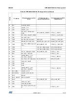
Page 72: ...15 OSC32_OUT OSC32_OUT 6 PF3 VBAT VBAT 7 PF4 VREF VREF 8 VDD_1 VDD 9 VSS_1 VSS 10 PF0 OSC_IN OSC_IN 11 PF1 OSC_OUT OSC_OUT 12 PF2 NRST NRST WKUP8 13 PC0 GPIO_EXT_RST 14 PC1 MC_IO_ PFC_sync1 GPIO_9V_EN_LPTIM1_OU T 15 PC2 GPIO_JOY_UP 16 PC3 GPIO_JOY_DOWN 17 PA0 JOY_SEL_TAMP_IN2 WKUP1 18 PA1 MC_AIN1_COMP_1_INP Bus voltage LDR_OUT_COMP_1_INP _ADC_IN1 GPIO_DP1_DET 19 PA2 MC_ADC_IN2 CurrentA SMART_2_TX ...

Page 73: ...GPIO_DISCHARGE_2 35 PB15 MC_IO_ Dissipative brake GPIO_SMART_3 5V TYPE C_1_CC2 36 PA8 MC_TIM_1_CH1 UH TYPE C_1_CC1 37 PA9 USART_BOOT_1_TX MC_TIM_1_CH2 VH TYPE C_1_DBCC1 38 PC6 MC_TIM_3_CH1 EncoderA IR_IN_TIM3_CH1 GPIO_DP2_HPD 39 PC7 GPIO_JOY_RIGHT 40 PD8 LED3 41 PD9 LED4 42 PA10 USART_BOOT_1_RX MC_TIM_1_CH3 WH TYPE C_1_DBCC2 43 PA11 PA9 USART_1_CTS 44 PA12 PA10 USART_1_RTS_DE_CK 45 PA13 SWDIO 46 P...

Page 74: ... LED2 57 PB3 LCD SD1_SCK 58 PB4 LCD SD1_MISO 59 PB5 MC_TIM_3_CH2 EncoderB TEMP_SENSOR_INT_W KUP6 GPIO_15V_EN 60 PB6 I2C1_SCL HDMI_SOURCE_I2C1_S CL MUX_I2C1_SCL 61 PB7 I2C1_SDA HDMI_SOURCE_I2C1_S DA MUX_I2C1_SDA 62 PB8 GPIO_LCD_CS 63 PB9 MC_IO_ NTC_bypass IR_OUT GPIO_VCONN_EN_1_2 64 PC10 VCP_USART_3_TX Table 40 STM32G081B EVAL IO Assignment continued Pin No Pin Name IO Assignment on mother board IO...

Page 75: ...reasonable protection against harmful interference when the equipment is operated in a commercial environment This equipment generates uses and can radiate radio frequency energy and if not installed and used in accordance with the instruction manual may cause harmful interference to radio communications Operation of this equipment in a residential area is likely to cause harmful interference in w...

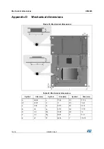
Page 76: ...sions Figure 53 Mechanical dimensions Table 41 Mechanical dimensions Symbol Size mm Symbol Size mm Symbol Size mm A 68 58 e 77 44 P2 111 76 A1 61 97 H 11 P3 10 41 a 2 54 Lx 5 715 Q1 24 12 B 36 Ly 5 715 Q2 17 70 D 3 5 Mx 19 08 Q3 16 d 3 2 My 23 81 X 114 3 E 47 P1 65 78 Y 172 72 ...

Page 77: ...UM2403 Rev 1 77 78 UM2403 Revision history 77 Revision history Table 42 Document revision history Date Revision Changes 7 Nov 2018 1 Initial version ...

Page 78: ...ers are solely responsible for the choice selection and use of ST products and ST assumes no liability for application assistance or the design of Purchasers products No license express or implied to any intellectual property right is granted by ST herein Resale of ST products with provisions different from the information set forth herein shall void any warranty granted by ST for such product ST ...

Reviews: