background image

ST7540 FSK powerline transceiver description

AN2451

10/55

Doc ID 12791 Rev 3

ST7540 FSK powerline transceiver description

ST7540 transceiver uses frequency shift keying (FSK) modulation to perform a half-duplex 
communication on a powerline network. It operates from a 7.5 to 13.5 V single supply 
voltage (Vcc) and integrates a power amplifier (PA), which is able to drive low line 
impedance, and two linear regulators providing 5 V and 3.3 V. 

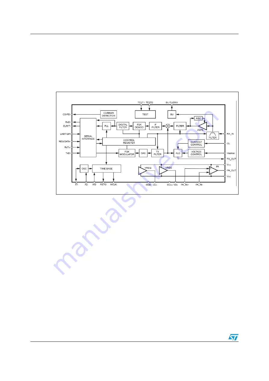
Figure 3.

ST7540 Transceiver block diagram

The ST7540 can communicate using eight different communication channels (60, 66, 72, 
76, 82.05, 86, 110, 132.5 kHz), four baud rates (600, 1200, 2400, 4800) and two deviations 
(1 and 0.5). Additional functions are included, such as watchdog, automatic control on PA 
output voltage and current, carrier/preamble detection and band-in-use signaling, 
transmission time-out, and thermal shutdown.

The transceiver, which is dedicated only to physical communication, operates with a 
microcontroller whose aim is to manage the communication protocol stack. A reset output 
(RSTO) and a programmable clock (MCLK) can be provided to the microcontroller by the 
ST7540 in order to simplify the external logic and circuitry.

The host controller can exchange data with the transceiver through a serial interface, 
programmable to operate either in UART (CLR/T data clock not used) or in SPI mode. 
Communication on the power line can be either synchronous or asynchronous to the data 
clock that is provided by the transceiver at the programmed baud rate. 

When in transmission mode (i.e. RxTx line at low level), the ST7540 samples the digital 
signal on the TxD line at the programmed baud rate and modulates it in a FSK sinusoidal 
output on the Tx_OUT line. This signal is then externally fed into the power amplifier to add 
current capability. The power amplifier can also introduce gain and active filtering to the 
signal, just using few external passive components. The resulting signal on the PA_OUT line 
is coupled to the power line. 

When in receiving mode (i.e. RxTx line at high level), an incoming FSK signal on the Rx_IN 
line is demodulated and the digital output is available for the microcontroller on the RxD pin. 

Summary of Contents for ST7540

Page 1: ...fically tailored to match powerline coupling requirements and to operate within a wide range of the input mains voltage Modem and crystal oscillator section Line coupling interface section The couplin...

Page 2: ...pedance 24 5 2 Conducted disturbances 25 5 2 1 Conducted emissions 25 5 2 2 Noise immunity 26 5 3 Thermal design 29 5 4 Oscillator section 32 5 5 Surge and burst protection 32 5 6 50 pin connector for...

Page 3: ...AN2451 Contents Doc ID 12791 Rev 3 3 55 Appendix A Board layout 51 List of normative references 54 Revision history 54...

Page 4: ...missions test setup 26 Figure 19 Output spectrum typical at 72 kHz 2400 baud deviation 1 mains 220Vac 26 Figure 20 Narrow band conducted interference test setup 27 Figure 21 Measured BER vs SNR curve...

Page 5: ...Vs AC_IN peak detector response 45 Figure 46 Example schematic for non isolated solution 46 Figure 47 Line coupling interface for 110 kHz channel 47 Figure 48 Line coupling interface for 132 5 kHz ch...

Page 6: ...Bill of materials 16 Table 4 ST parts on the ST7540 reference design board 18 Table 5 Line coupling transformer specifications 21 Table 6 Noise immunity test settings 27 Table 7 50 pin connector digi...

Page 7: ...onic distortion at mains output Loaded with CISPR 16 1 network 55 dBC 3rd harmonic distortion at mains output Loaded with CISPR 16 1 network 61 50Hz attenuation 100 dB Receiving specifications Rx mode...

Page 8: ...0 kHz Table 1 Electrical characteristics of the ST7540 reference design continued Parameter Test conditions Value Unit Min Typ Max Table 2 Output voltage level setting through Vsense partitioning typi...

Page 9: ...mains none of the live parts should be touched immediately because of the energized capacitors It is mandatory to use a mains insulation transformer to perform any tests on the high voltage sections s...

Page 10: ...he communication protocol stack A reset output RSTO and a programmable clock MCLK can be provided to the microcontroller by the ST7540 in order to simplify the external logic and circuitry The host co...

Page 11: ...7540 power line modem demo kit software tool one EVALCOMMBOARD hosting the ST7 microcontroller one ST7540 reference design board EVALST7540 2 The correct procedure for connecting the EVALST7540 2 and...

Page 12: ...xact transmitted bit sequence This can be done in two ways via the ST7540 control register settings the internal configuration register of the modem has a frame header field in which an 8 or 16 bit he...

Page 13: ...r to plug the mains supply on one side of it and the I B U communication board on the other side Figure 6 Positioning of the various sections of the board The schematics of the whole reference design...

Page 14: ...Board description AN2451 14 55 Doc ID 12791 Rev 3 Figure 7 Modem and coupling interface schematic HIGH VOLTAGE SECTION...

Page 15: ...16V R2 220k R2 220k R5 1k5 R5 1k5 R1 10R 1W R1 10R 1W L3 470uH L3 470uH 2 1 D4 D4 R3 10 K R3 10 K 1 3 2 D5 10V D5 10V C3 10uF 400V C3 10uF 400V L4 33 uH L4 33 uH 1 2 4 3 U2 U2 2 4 1 3 6 5 7 8 U1 U1 4...

Page 16: ...2 C11 C12 33pF TDK C1005C0G 1H330J 13 2 C14 C27 10nF Murata GRM188R7 1H103K 14 4 C16 C18 C19 C25 100nF TDK C1608X7R 1H104K 15 2 C21 C33 150pF Murata GRM1885C 1H151J 16 1 C22 10uF Murata GRM21BR6 1A106...

Page 17: ...03 1 43 1 R4 560 0603 1 44 1 R5 1K5 0603 1 45 1 R6 1K1 0603 1 46 1 R7 47K 0603 1 47 1 R8 15K 0603 1 48 1 R9 4K7 0603 1 49 1 R10 12K 0603 1 50 1 R12 1K 0603 1 51 1 R14 1K8 0603 1 52 1 R17 470 0603 1 53...

Page 18: ...2 capacitor 1 for SMD resistors 5 for SMD ceramic capacitors To evaluate sensitivity of the filters to the tolerances listed above the following sections include simulated responses of the filters wit...

Page 19: ...s stage and a Sallen Key 2 pole cell with 9dB gain The R19 C32 low pass stage is aimed at introducing attenuation starting from approximately an octave above the transmission channel frequency The tra...

Page 20: ...rance effect 5 1 2 Tx passive filter Coupling to the power line requires some passive components in addition to the active filtering stage In particular Tx passive filter section is made of the decoup...

Page 21: ...er without inserting series inductance L5 L6 The drawback however is the poor accuracy of this parameter which can lead to a shift of the filter response and to bad coupling Consequently a low leakage...

Page 22: ...d to the CISPR network with the components tolerance effect 5 1 3 Rx passive filter The Rx filter is made up of a resistor in series with a parallel L C resonant The transfer function of the filter ca...

Page 23: ...transfer if RL is set to zero Looking at the first way to express the module of the transfer function it is possible to notice that a higher value of Q can help keeping the losses small Nevertheless a...

Page 24: ...s in both Tx and Rx mode In both figures channel impedance point and the minimum impedance point are indicated The impedance magnitude values prove that the ST7540 reference design board is compliant...

Page 25: ...bances 5 2 1 Conducted emissions The EN50065 1 standard describes the test setup and procedures for testing conducted emissions The conducted emissions measurements have been taken with 220 Vac mains...

Page 26: ...k traced in red may be compared to the typical output spectrum of the ST7540 reference design board Figure 19 Output spectrum typical at 72 kHz 2400 baud deviation 1 mains 220Vac 5 2 2 Noise immunity...

Page 27: ...trum Analyzer allows measurement of the actual signal and noise levels as seen by the receiving ST7540 internal circuitry programmed for 2400 baud Figure 21 represents the BER vs SNR curve in the pres...

Page 28: ...ulated signal has been decreased until the measured BER was lower than 10 3 one error every 1000 transmitted bits Figure 22 shows SNR vs frequency curves for both a pure sinusoidal and an AM modulated...

Page 29: ...issipating area on the bottom side is nearly 1 5 cm2 Figure 23 PCB copper dissipating area for ST7540 reference design board Even if the ST7540 features a built in thermal shutdown circuitry which tur...

Page 30: ...wer that is well above the one sustainable at steady state For this reason a complete thermal analysis requires taking into account the characteristics of the transmission i e duty cycle and duration...

Page 31: ...40 reference design Figure 27 Dissipated power vs load impedance modulus typical curve for ST7540 reference design board Referring to the relationship between dissipated power and temperature it can b...

Page 32: ...apacitors No tracks or vias should cross the ground plane except for the crystal connections It is also recommended to use a large clearance on the oscillator related tracks to minimize humidity probl...

Page 33: ...e 1 2 x 50 s Fast transient burst tests are specified at level 2 kV with pulse shape 5 x 50 ns and pulse frequency 5 kHz Figure 29 Figure 30 and Figure 31 illustrate the protection criteria implemente...

Page 34: ...Board description AN2451 34 55 Doc ID 12791 Rev 3 Figure 30 Common mode disturbances protection negative disturbance Figure 31 Differential mode disturbances protection...

Page 35: ...ode An Analog Input ANALOG_IN which is a line intended to implement a Received Signal Strength Indicator a peak meter used to give an Rx signal level estimation A VDDF_FORCE signal which forces the mi...

Page 36: ...cup mode The power supply is designed in isolated flyback configuration Secondary regulation implemented through an optocoupler and a Zener diode takes the requested output tolerance for the specified...

Page 37: ...ke the maximum reverse voltage and the RMS secondary current into account A STPS1H100 Power Schottky rectifier has been chosen for this purpose A LC filter has been added on the output consisting of L...

Page 38: ...on stops the device operation until the device temperature falls The startup phase could be critical for the SMPS Output overshoot occurs if the circuit is not properly designed Care must be taken in...

Page 39: ...6 Typical waveforms at 265 Vac startup Ch1 freq 23 50 Hz green Ch4 max 2 08 A light blue Ch4 mean 383 mA light blue Ch1 max 702 V black Ch2 mean 19 72 V green Ch4 max 500 mA light blue VDS IOUT VDD 11...

Page 40: ...and the VIPer are forced to operate close to their current limitations and thus the efficiency is reduced In general efficiency is affected by the losses which are due to R1 series input resistor lim...

Page 41: ...master node The main characteristics of this tool are indicated in red Figure 39 ST7540 powerline modem demonstration kit window for the master board Special controls are included in the ping test Re...

Page 42: ...ach meter is placed on This information is mainly useful at system level in order to check for unexpected losses on the distribution line due to failures or energy theft Since the three phases on the...

Page 43: ...h a current flowing into the LED of the optocoupler can minimize the delay between the actual zero crossing of the mains voltage and the edge of the ZC_OUT signal if the optocoupler has been chosen to...

Page 44: ...of the incoming signal is useful to Evaluate the SNR signal to noise ratio at the node Choose the best routing through the network if repeaters are allowed One possible implementation for the receive...

Page 45: ...ure sinusoidal waveform at the input The DC_OUT signal should be converted through an integrated A D converter by the application microcontroller Figure 45 Measured DC_OUT Vs AC_IN peak detector respo...

Page 46: ...the ac dc SMPS For example the L5970 DC DC step down switching regulator can be used in case of 24 V bus to obtain the 12 V supply for the ST7540 device 7 6 110 and 132 5 kHz coupling circuit In this...

Page 47: ...AN2451 Application ideas Doc ID 12791 Rev 3 47 55 Figure 47 Line coupling interface for 110 kHz channel...

Page 48: ...Application ideas AN2451 48 55 Doc ID 12791 Rev 3 Figure 48 Line coupling interface for 132 5 kHz channel...

Page 49: ...transmit What to check a Check the voltage on the PA_OUT test pad with the oscilloscope ground probe connected to the SVss signal ground The programmed carrier frequency must be present on the PA_OUT...

Page 50: ...k if data are present on the RxD pin 6 Problem during a ping test or a transmission test the ST7540 reference design board shows high bit error rate Note This point refers to a half duplex communicati...

Page 51: ...AN2451 Board layout Doc ID 12791 Rev 3 51 55 Appendix A Board layout Figure 49 PCB layout component placing...

Page 52: ...Board layout AN2451 52 55 Doc ID 12791 Rev 3 Figure 50 PCB layout top view...

Page 53: ...AN2451 Board layout Doc ID 12791 Rev 3 53 55 Figure 51 PCB layout bottom view...

Page 54: ...ty requirements Part 4 2 Low voltage decoupling filters safety requirements Part 7 Equipment impedance Revision history Table 12 Document revision history Date Revision Changes 10 Jan 2007 1 First iss...

Page 55: ...ARRANTIES OF MERCHANTABILITY FITNESS FOR A PARTICULAR PURPOSE AND THEIR EQUIVALENTS UNDER THE LAWS OF ANY JURISDICTION OR INFRINGEMENT OF ANY PATENT COPYRIGHT OR OTHER INTELLECTUAL PROPERTY RIGHT UNLE...

Reviews: