


Hardware (designing PCB schematics and layout)
AN4450
10/26
DocID025978 Rev 1
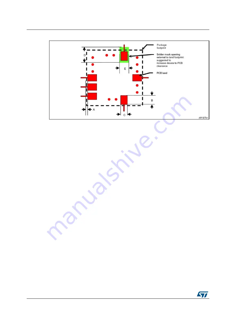
Figure 6. Recommended land and solder mask design for *LGA packages
A = Clearance from PCB land edge to solder mask opening
≥
0.25 mm to ensure that
solder mask is opened externally to device area
B = PCB land length = *LGA solder pad 0.1 mm
C = land width = *LGA solder pad width + 0.1 mm
D = Solder mask opening length = PCB land 0.3 mm: design 0.05 mm inside
and 0.25 mm outside
E = Solder mask opening width = PCB land width + 0.1 mm
2.2.2
Stencil design and solder paste application
The soldering paste thickness and pattern are important for a proper pressure sensor
mounting process.
Stainless steel stencils are recommended
Stencil thickness of 90 - 150 µm (3.5 - 6 mils) is recommended for screen printing
The final soldering paste thickness should allow proper cleaning of flux residues and
clearance between sensor package and PCB
Stencil aperture should have a rectangular shape with dimensions up to 25 µm (1 mil)
smaller than PCB land
The openings of the stencil for the signal pads should be between 70 - 80% of the PCB
pad area
Optionally, for better solder paste release, the aperture walls should be trapezoidal and
the corners rounded
The fine IC leads pitch requires accurate alignment of the stencil to the PCB. The
stencil and printed circuit assembly should be aligned to within 25 µm (1 mil) prior to
application of the solder paste
2.2.3 Process
consideration
In using non self-cleaning solder paste, proper board washing after soldering must be
carried out to remove any possible sources of leakage between pads due to flux residues.
However, take care not to perform the cleaning process on top of the pressure sensor.


