background image

December 2012

Doc ID 022934 Rev 1

1/53

AN4070

Application note

250 W grid connected microinverter

By Rosario Attanasio

Introduction

This application note describes the implementation of a 250 W grid connected DC-AC 
system suitable for operation with standard photovoltaic (PV) modules. The design is 
associated to the STEVAL-ISV003V1 demonstration board which demonstrates the 
possibility of implementing a full microinverter solution (MIC) using STMicroelectronics 
products.

In fact, both the components used to implement the power, control and communication 
section belong to the product portfolio offered by STMicroelectronics. 

The design is based on two power stages, namely, an interleaved isolated boost DC-DC 
converter and a mixed frequency DC-AC converter. The control section is based on an 
STM32F103xx microcontroller which ensures proper maximum power point tracking 
(MPPT) on the input side of the system and decoupled control of the active and reactive 
power on the output. The control algorithm has been developed to allow system operation 
both with 230 V AC, 50 Hz grids and with 240 V AC, 60 Hz without any hardware 
modifications. The connection to a 120 V AC, 50/60 Hz grid requires few hardware 
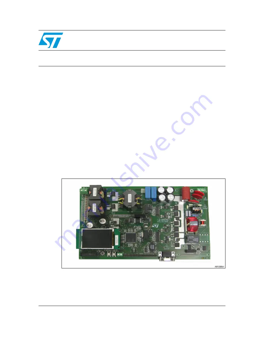
modifications to ensure the best system performance. An image of the STEVAL-ISV003V1 
demonstration board is shown in 

Figure 1

Figure 1.

Image of the 250 W MIC

www.st.com

Summary of Contents for AN4070

Page 1: ...t portfolio offered by STMicroelectronics The design is based on two power stages namely an interleaved isolated boost DC DC converter and a mixed frequency DC AC converter The control section is based on an STM32F103xx microcontroller which ensures proper maximum power point tracking MPPT on the input side of the system and decoupled control of the active and reactive power on the output The cont...

Page 2: ...esign 7 3 Schematic description 20 4 STM32F103xx based current control for inverter grid connection 29 5 Experimental test results 35 Appendix A Magnetic components datasheets 42 Appendix B Alternative DC DC converter magnetic components with low profile 49 6 Conclusions 51 Revision history 52 ...

Page 3: ...main specifications 10 Table 3 DC DC converter MOSFET main characteristics 13 Table 4 DC DC converter rectifier diodes main characteristics 13 Table 5 HF transformer specifications 14 Table 6 RM14 core with N87 Ferrite main characteristics 15 Table 7 STB11N65M5 MOSFET main electrical characteristics 19 Table 8 Document revision history 52 ...

Page 4: ...e 30 Figure 21 Block diagram of the control algorithm implemented on the 250 W MIC STM32F103xx 32 Figure 22 DC DC converter MOSFET current green and drain to source voltage purple 250 W35 Figure 23 DC DC converter input current ripple cancellation and inductor currents 36 Figure 24 DC DC converter HF transformer waveforms 36 Figure 25 DC DC converter rectifier diode waveforms 37 Figure 26 Inverter...

Page 5: ...m power point tracking MPPT High efficiency and high input to output voltage step ratio are the most important requirements for this stage High voltage gain can be obtained through capacitor multiplier systems or high frequency transformers but since galvanic isolation is required for MIC applications the HF transformer is always necessary The transformer turns ratio depends on the input and outpu...

Page 6: ...put and the output of the system Finally the input current generated by the PV module is sensed using a simple current shunt resistor These five feedback signals are sampled at 17 4 kHz using the STM32F103xx 12 bit A D converters The control strategy is based on a standard perturb and observe P O MPPT algorithm to adapt the input system impedance to the PV module electrical characteristics while i...

Page 7: ...ls used to command the two MOSFET gates are 180 degree phase shifted with respect to each other and always have a duty cycle 0 5 This introduces the problem of controlling the DC DC operation at very low output power Two solutions can be used to overcome this problem With the first solution the DC DC converter is controlled by keeping the duty cycle at the minimum allowable value and the switching...

Page 8: ...verlapped during part of the switching period there is an operating interval during which both the MOSFET devices are ON and therefore both the input inductor chokes L1 and L2 store energy During this interval the input current is equally divided in the two MOSFETs as shown in Figure 6 and no current flows across the secondary winding and the diodes The load is supplied by the output capacitors DW...

Page 9: ...2 is in conduction Figure 7 During the third time interval both MOSFETs conduct again Therefore energy is stored both in L1 and L2 while the load is supplied by the output capacitors During the fourth time interval MOS1 is off and MOS2 is kept on which means that the energy previously stored in L1 is discharged on C3 with the transformer secondary current flowing through D1 In reality some additio...

Page 10: ...described and commented on in the following part of this document 1 Calculation of the switching period Equation 1 Table 2 DC DC converter main specifications Specification Value Nominal input voltage 35 8 V Maximum input voltage 40 V Minimum input voltage 20 V Nominal output power 250 W Nominal output voltage 380 V Maximum output voltage 430 V Minimum output voltage 370 V Target efficiency 97 Swi...

Page 11: ...Equation 6 7 Calculation of transformer turns ratio Equation 7 where Vin is chosen as the average between the maximum and minimum input voltage value The final transformer turns ratio has been chosen equal to 2 6 8 Calculation of minimum current value for CCM operation Equation 8 to ensure CCM for I Ilim s on s on T t T t D 7 0 2 0 5 0 max max max 1 2 0 1 2 N N D V V in W P P out in 7 257 97 0 250...

Page 12: ...rrent Equation 13 14 Calculation of maximum capacitor ESR Equation 14 15 Calculation of main power devices breakdown voltage Equation 15 A I I A I I A I I in ripple ind in ind 15 0 2 31 0 2 31 0 2 625 0 lim Δ Δ Δ Δ uH f I D V L A I I s ind switch in in ind 640 625 0 2 max _ min _ Δ Δ Δ A n I D I in rms D 3 3 6 2 2 8 12 2 0 2 2 2 max max uF V T D I C s o 92 1 2 0 10 57 28 2 0 675 0 6 max Δ ΔIcap Ii...

Page 13: ...SFET 4 5 mΩ 106 8 ns 100 V 120 A 114 6 nC Table 4 DC DC converter rectifier diodes main characteristics Device Type Vf 12 A Trr Vbr Id 100 C IRM typ STTH12R06 Ultrafast soft recovery 1 4 V 25 ns 600 V 12 A 7 A V V V out diode brdw 516 430 2 1 2 1 max Ω Δ Δ Δ Δ Δ 96 2 675 0 2 10 6 9 2 35000 675 0 35000 max min c c C in c c c in i V ESR V V uF V i C in W P P P P W f Q V P W I R P W T t I V P drv con...

Page 14: ...The design procedure and equations are shown in the section below 1 Calculation of total transformer power Equation 20 Table 5 HF transformer specifications Specification Value Turns ratio 2 6 RMS input current 4 7 A Nominal output voltage 380 V Minimum output voltage 370 V Output current 1 77 A Switching frequency 35 kHz Efficiency 98 Max operating flux density 0 05T Window utilization 0 3 Duty c...

Page 15: ...uming a maximum flux density swing of 200 mT the minimum number of primary turns to avoid core saturation is given by Equation 22 5 Calculation of the magnetizing inductance Equation 23 6 Wire size calculation At 35 kHz the current penetration depth is given by Equation 24 Table 6 RM14 core with N87 Ferrite main characteristics Specification Value Equivalent core section area Ac 170 mm2 Core volum...

Page 16: ...th can be calculated using the following equations Equation 28 Knowing that copper resistivity ρ is equal to Equation 29 The primary and secondary winding resistance values are given by Equation 30 7 Transformer losses calculation Having calculated the values of primary and secondary winding resistance the calculation of copper losses is straightforward with the following equation Equation 31 mm d...

Page 17: ...S6 are connected in one leg and switch at a frequency of 17 4 kHz Two Schottky diodes are connected to the drain of these two MOSFETs in order to inhibit the internal body diode Two external silicon carbide SiC diodes are therefore connected in anti parallel for current freewheeling while avoiding problems connected to reverse recovery at MOSFET turn on MOS7 and MOS 8 are connected in the second l...

Page 18: ...lculate the filtering inductance value Equation 36 where n is the number of inverter levels Vbus 0 and Vbus and D is the inverter duty cycle The filter capacitor value is selected to limit the exchange of reactive power below 5 of nominal active power Equation 37 To avoid resonance problems for the filter due to low and high order harmonics the resonant frequency should be chosen in a range betwee...

Page 19: ...entioned above The four MOSFETs selected for the inverter stage are 9 A 650 V MDMeshV devices The part number is STB11N65M5 and the main electrical characteristics are reported in Table 7 The blocking diodes are two STPS1545 15 A 45 V Schottky diodes while the freewheeling diodes are two STPSC606 6 A 600 V silicon carbides Table 7 STB11N65M5 MOSFET main electrical characteristics Device Type RDSma...

Page 20: ...e driving network of the high frequency leg devices to ensure sinusoidal output current and voltage waveforms The inverter is interfaced to the grid via an LCL filter A relay is used to connect and disconnect the inverter from the grid whenever required by the application The schematic in Figure 11 shows the filtering and relay schematic section The grid current feedback signal is obtained using a...

Page 21: ...pply connected to the PV input The schematic of the auxiliary power supply is shown in Figure 14 The two L4971s are connected to few external components in order to implement two buck converters used to step down the input voltage to 15 V and to 5 V The 3 3 V supplying the STM32F103xx microcontroller is then generated from the 5 V using a standard linear regulator The 3 3 V is also used to supply ...

Page 22: ...8 5 5 P2KP 5 X 9 6736 8 5 6 16 60 60 6736 8 5 5 3CHOTTKY 6736 8 5 N X 9 7 2 15 9 2 15 9 5 S 9 5 N RZ I 3 0 LJK 6LGH X 9 9 1B6 16B39 4 67 1 0 4 67 1 0 AGNETICA U 9 1387 6736 8 5 5 6FKRWWN 6736 8 X 9 6736 4 67 1 B6 16B39 X 9 1 8 725 DWH LJK I 3 0 RZ 6LGH AGNETICA U LJK I 3 0 LJK 6LGH 4 67 1 RZ I 3 0 RZ 6LGH 6736 X 9 5 X 9 5 1 026 7 5 1 026 7 X 9 X 9 9 DWH 6736 8 287 5 287 X 9 X 9 X 9 X 9 X 9 6736 8 ...

Page 23: ...Rev 1 23 53 Figure 11 Schematic of the filtering and relay circuit V 5 1 Q 9 287 Q 9 6736 8 6 7029 53 86 6 7029 53 57 5281 1 875 BVHQV BVHQV 5 B1 87 4 1 5 7 P 5 N 9FF 9 6 9 5 1 Q 9 Q 9 21 5 Q 9 RLOFUDI W 8 5 5 X 9 5 B 5 5 0DJQHWLFD 0DJQHWLFD 287 ...

Page 24: ...Schematic description AN4070 24 53 Doc ID 022934 Rev 1 Figure 12 DC DC converter driver V 9FF 9 DWH 3 0 3 0 DWH 5 RKP 5 RKP X 9 30 1 1 3 0 1 3 0 287 9 287 ...

Page 25: ...9 227 9 287 1 1 9 23 3 5 N 5 N X 9 5 RKP X 9 30 1 1 3 0 1 3 0 287 9 287 5 RKP X 9 30 1 1 3 0 1 3 0 287 9 287 RZ I 3 0 LJK 6LGH 287 6 16 RZ I 3 0 RZ 6LGH 8 1 6 2 1 9FF 7 23 23287 1 9 227 9 287 1 1 9 23 3 5 N LJK I 3 0 RZ 6LGH 5 N X 9 X 9 X 9 3 1 7 2 9 12 9 1 1 92 X 9 9 P 5 3 1 7 2 9 12 9 1 1 92 9 P 5 5 N 3 0 109 6 9FF 9 QG 5 N 3 0 109 6 9FF 9 QG Q 9 Q 9 Q 9 Q 9 B9FF 9 B9FF 9 9FF 9 B9FF 9 677 B9FF 9...

Page 26: ...urrent sensing V 6CC 6 0 3 1 N N 0 3 0 2 K 3403 5 0 7 2 3500 9 6 OILCRAF T 33 5 SC OMP 54 6CC 33 6FB OOT 2 K N P 2 2 U 6 N 6 054 U 6 N N 0 3 1 N 0 3 0 N 2 K 3403 5 33 0 7 2 3500 9 6 OILCRAF T 2 K 5 SC OMP 54 6CC 33 6FB OOT N 2 P 2 U 6 6 054 N N U 6 N 6CC 6 V 2 2 43 54 N 6CC N 54 6CC N N INE CURRENT OUT SENS 2 2 K 2 522 4 3 3 2 N 6CC 6 ...

Page 27: ...AN4070 Schematic description Doc ID 022934 Rev 1 27 53 Figure 16 AC line voltage sensing 8 76 5 N 5 N Q 9 B LQH YROWDJH Q 9 5 N 5 N Q 9 9FF 9 BVHQV 9FF 9 1 875 BVHQV 7 WDFRLO 69 5 5 5 6 ...

Page 28: ...n AN4070 28 53 Doc ID 022934 Rev 1 Figure 17 PV current sensing Figure 18 PV voltage sensing V 2 N 0 522 4 3 3 06 43 54 N 6CC N 54 6CC N N N 6CC 6 2 K 2 K V 2 K 0 6 4 6 3 3 06 2 K N 43 54 N 6CC N 54 6CC N N N 2 K 2 K 6CC 6 ...

Page 29: ...d phase angle The detection method used in this implementation for a single phase inverter is based on a synchronous reference frame PLL Single phase inverters require a virtual bi phase system In fact to create a rotating d q reference starting from a stationary frame at least two independent phases are required This problem is overcome with the creation of a virtual voltage Vβ phase shifted with...

Page 30: ... and Vq One of the two components is controlled to zero with a PI regulator The output of the PI regulator is the grid frequency which can be integrated to obtain the grid angle It is worth noting that if the Vq component is controlled to zero then the Vd component follows the grid voltage rotation In this case the active power injected into the grid can be θ θ θ θ α β q d V V cos sin sin cos V V ...

Page 31: ...mmand and the actual estimated value The difference between the reference components of the current and the actual d q components are the inputs of the PI regulators in the inner control loop The outputs of the PI regulators in the inner loop are two voltage components Vd and Vq By performing a reverse Park transformation two AC voltages are generated back on the stationary reference frame and so ...

Page 32: ...he bus DC reference voltage The minimum DC bus voltage is a function of the peak to peak AC line voltage in order to minimize the total harmonic distortion THD of the injected current This limit depends on grid voltage fluctuations and can be calculated according to the following equation Equation 44 where Pdc is the average power on the DC bus Vgrid_max is the maximum RMS value of the grid voltag...

Page 33: ...ercurrent Due to fault conditions or AC line transient conditions the maximum current may be exceeded In this case the inverter ceases to deliver power to the grid The current threshold value is set to 1 2 A The demonstration board is provided with the components required to implement hardware short circuit protection However this protection is disabled and may be activated by properly sizing the ...

Page 34: ... ID 022934 Rev 1 The tuning of the PI regulators can be performed using the specific function implemented in the control algorithm Acting on the two current regulators is very effective in order to adjust the quality of the output current both in terms of total harmonic distortion ...

Page 35: ...oinverter was operating at 250 W of output power with an input voltage of 30 V Figure 23 shows the current flowing through each of the two input inductors and the effect of current ripple cancellation that the interleaving has on the converter input current blue track when the system is operating at 30 V input and 250 W output power The HF transformer main waveforms are reported in Figure 24 where...

Page 36: ...Experimental test results AN4070 36 53 Doc ID 022934 Rev 1 Figure 23 DC DC converter input current ripple cancellation and inductor currents Figure 24 DC DC converter HF transformer waveforms ...

Page 37: ...evice is then used to generate the two complementary signals controlling the gate of each STB11N65M5 MOSFET in the bridge The resulting output voltage and current waveforms are shown in Figure 27 where the purple track is the voltage between the mid points of each leg the blue track is the system output voltage on the filter output and the green track is the system output current The efficiency of...

Page 38: ...C output waveforms when operating in open loop mode Figure 30 shows the same waveforms when the system is operating at nominal power in closed loop mode and grid connection In these operating conditions the current THD is 2 8 When operating in grid connection the current THD is higher and equal to 4 8 at full load while the power factor is equal to 0 92 Figure 30 shows the current and voltage wave...

Page 39: ...AN4070 Experimental test results Doc ID 022934 Rev 1 39 53 Figure 28 DC DC converter efficiency Figure 29 Microinverter efficiency V IILFLHQF 2XWSXW 3RZHU IILFLHQF 9LQ 9 V IILFLHQF 2XWSXW 3RZHU ...

Page 40: ...Experimental test results AN4070 40 53 Doc ID 022934 Rev 1 Figure 30 MIC output current and voltage waveforms during grid connection Figure 31 Output current THD V XUUHQW 7 2XWSXW 3RZHU ...

Page 41: ...AN4070 Experimental test results Doc ID 022934 Rev 1 41 53 Figure 32 Power factor V 3RZHU IDFWRU 2XWSXW 3RZHU ...

Page 42: ...ATIONS TECHNICAL DATA INDUCTANCE 600 uH 15 MEASURE 1KHZ TA 20 C RESISTANCE 81 mΩ MAX MEASURE DC TA 20 C OPERATING CURRENT 4 A MAX MEASURE DC TA 20 C SATURATION CURRENT 6 5 AMAX MEASURE DC L 50 NOM TA 20 C RESONANCE FREQUENCY 637 KHZ NOM TA 20 C OPERATING TEMPERATURE RANGE 10 C 65 C IR 4A MAX THERMAL CLASS B MAXIMUM DIMENSIONS 35 X33 H 33 mm WEIGHT 90 g APPROX CIRCUIT DIAGRAM INDUCTANCE VS CURRENT ...

Page 43: ...600uH 4A Class Code 2162 0003 Customer STMICROELECTRONICS Customer Code Date 24 11 2010 Revision 0 Page 2 of 2 MOR D0014 00 Rev 00 02 09 08 MAGNETICA DIMENSIONAL DRAWING DIMENSIONS IN MILLIMETERS DRAWING NOT IN SCALE 0 8 X11 RECOMMENDED PCB HOLE 1 2 X11 BOTTOM VIEW PIN SIDE 35 MAX 5 7 1 2 3 4 5 7 33 MAX 33 MAX 2 3 4 12 11 10 9 8 7 7 6 5 1 30 5 1 5 MISSING PIN 6 REFERENCE AS PCB ASSEMBLING ...

Page 44: ...Magnetic components datasheets AN4070 44 53 Doc ID 022934 Rev 1 Figure 35 AC voltage TV AM12182v1 0 0 ...

Page 45: ...TRANSFORMER RATIO MEASURE 10KHZ TA 20 C PIN 12 10 4 5 6 1 2 3 1 33 3 PIN 9 7 4 5 6 1 2 3 1 33 3 LEAKAGE INDUCTANCE 0 41 uH NOM MEASURE 4 5 6 1 2 3 AND 7 9 10 12 IN S C F 10KHZ TA 20 C PARASITIC CAPACITANCE 13 pF NOM MEASURE 4 5 6 1 2 3 WITH 7 9 10 12 IN OC F 1MHZ TA 20 C OPERATING CURRENT 4 AP MAX MEASURE 4 5 6 1 2 3 PMAX 250W F 50KHZ TA 20 C OPERATING FREQUENCY 50 KHZ NOM PMAX 250W TA 20 C OPERAT...

Page 46: ...H 200V Class Code 2159 0003 Customer STMICROELECTRONICS Customer code Date 12 01 11 Revision 01 Page 2 of 2 MOR D0014 00 Rev 00 02 09 08 MAGNETICA DIMENSIONAL DRAWING DIMENSIONS IN MILLIMETERS DRAWING NOT IN SCALE 42 MAX 31 MAX 3 MIN 43 MAX REFERENCE PIN 1 12 1 1 2 3 4 5 6 TOP VIEW LAYOUT VIEW IN MOUNTIG DIRECTION 2 54 35 56 27 94 5 08 7 62 1 X12 RECOMMENDED PCB HOLE 1 6 X12 4 5 6 BOTTOM VIEW PIN ...

Page 47: ...RIDGE APPLICATIONS TECHNICAL DATA INDUCTANCE MEASURE 1KH Z TA 20 C PIN 1 4 3 6 mH 15 R ESISTANCE MEASUREDC TA 20 C PIN 1 4 292 m MAX OPERATING CURRENT 1 5 A MAX MEASURE DC TA 20 C SATURATION CURRENT 1 77 AP MEASUREDC L 50 NOM TA 20 C R ESONANCE FREQUENCY 589 KHZ NOM T A 20 C AMBIENT TEMPERAT URE R ANGE 20 C 85 C IR 1 5 A MAX WITH SELF TRISE 45 C THERMAL CLASS B S TORAGE TEMPERAT URE R ANGE 20 C 85...

Page 48: ...tor 3 6mH Class Code 2196 0001 Date 24 05 2011 Revision 0 Page 2 of 2 MOR D0014 00 Rev 00 02 09 08 MAGNETICA DIMENSIONAL DRAWING DIMENSIONS IN MILLIMETERS DRAWING NOT IN SCALE BOTTOM VIEW PIN SIDE 1 26 5 MAX 4 1 0 5 22 MAX 3 12 75 3 3 1 75 5 5 5 12 13 17 3 2 2 TOP VIEW GRID 2 4 2 4 5 5 5 3 5 12 75 9 8 14 6 34 MAX 21 MAX 3 8 MAX 1 6 0 1 0 2 1 4 0 71 X4 RECOMMENDED PCB HOLE 1 1 X4 ...

Page 49: ...C DC converter magnetic components with low profile Doc ID 022934 Rev 1 49 53 Appendix B Alternative DC DC converter magnetic components with low profile Figure 40 DC DC inductor for 250 W microinverter AM15526v1 B 5 H X Y ...

Page 50: ...Alternative DC DC converter magnetic components with low profile AN4070 50 53 Doc ID 022934 Rev 1 Figure 41 DC DC transformer for 250 W microinverter AM15527v1 B H X Y ...

Page 51: ...pability This is the main reason why the power conversion is based on a dual stage topology rather than the more common single stage one The converter performs MPPT and grid connection by means of an ARM Cortex M3 based microcontroller STM32F103xx which is well proven to be perfectly suited for PV applications Simulation and experimental results have confirmed the consistency of the proposed solut...

Page 52: ...Revision history AN4070 52 53 Doc ID 022934 Rev 1 Revision history Table 8 Document revision history Date Revision Changes 12 Dec 2012 1 Initial release ...

Page 53: ...ARRANTIES OF MERCHANTABILITY FITNESS FOR A PARTICULAR PURPOSE AND THEIR EQUIVALENTS UNDER THE LAWS OF ANY JURISDICTION OR INFRINGEMENT OF ANY PATENT COPYRIGHT OR OTHER INTELLECTUAL PROPERTY RIGHT UNLESS EXPRESSLY APPROVED IN WRITING BY TWO AUTHORIZED ST REPRESENTATIVES ST PRODUCTS ARE NOT RECOMMENDED AUTHORIZED OR WARRANTED FOR USE IN MILITARY AIR CRAFT SPACE LIFE SAVING OR LIFE SUSTAINING APPLICA...

Reviews: