background image

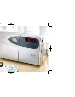
SRF-M37

E Model

SERVICE MANUAL

FM STEREO/AM PLL SYNTHESIZED RADIO

SPECIFICATIONS

Ver 1.0  2003. 03

Sony Corporation

Personal Audio Company

Published by Sony Engineering Corporation

9-877-168-01

2003C167800-1

© 2003.03

Time display:

24-hour system

Frequency range

Band

SRF-M37

Channel step

FM

87.5-108 MHz

0.1 MHz

AM

530-1


710 kHz

10 kHz

531-1


710 kHz

9 kHz

Output

i

 jack (ø 3.5 mm, stereo minijack) load impedance 24 

 (North

American model), 16 

 (Other models)

Power output

2.8 mW + 2.8 mW (at 10 % harmonic distortion)

Power requirements

1.5 V DC, one R03 (size AAA) battery

Dimensions

Approx. 83 

×

 63 

×

 32 mm (w/h/d)

(3 

3

/

8


×

 2 

1

/

2


×

 1 

5

/

16

 inches) incl. projecting parts and controls

Approx. 83 

×

 63 

×

 25 mm (w/h/d)

(3 

3

/

8


×

 2 

1

/

2

×

 1 inches) not incl. projecting parts and controls

Mass

Approx. 94 g (3.32 oz.) incl. battery and belt clip.

Accessories Supplied

Stereo headphones (1): North American model
Stereo earphones (1): Other models
Belt Clip (1)

Design and specifications are subject to change without notice.

Battery Life

 (Approx. hours)

(JEITA*)

When using

FM

AM

MW/LW

Sony alkaline

35

52

52

LR 03 (size AAA)
Sony R03 (size AAA)

14

21

21

* Measured by JEITA (Japan Electronics and Information Technology

Industries Association) standards. The actual battery life may vary
depending on the circumstance of the unit.

Summary of Contents for Walkman SRF-M37

Page 1: ...5 V DC one R03 size AAA battery Dimensions Approx 83 63 32 mm w h d 3 3 8 2 1 2 1 5 16 inches incl projecting parts and controls Approx 83 63 25 mm w h d 3 3 8 2 1 2 1 inches not incl projecting parts and controls Mass Approx 94 g 3 32 oz incl battery and belt clip Accessories Supplied Stereo headphones 1 North American model Stereo earphones 1 Other models Belt Clip 1 Design and specifications ar...

Page 2: ... CLOCK TUNE TIME SET PRESET TUNING 1 6 BAND FM SENS DX LOCAL i jack Prise i Buchse i 1 Setting the Clock The display will flash AM 12 00 or 0 00 when the battery is first inserted 1 Hold down CLOCK for more than 2 seconds The beep sounds and the hour flashes in the display 2 Press TUNE TIME SET or until the correct hour appears in the display Each press changes the digit s by one When you keep the...

Page 3: ...sembly procedure in the numerical order given 2 1 Cabinet Front Assy CABINET FRONT ASSY KEY BOARD ASSY MAIN BOARD ASSY SET This set can be disassembled in the order shown below 2 four tapping screws B 1 7 6 3 cabinet front assy 1 Open the battery case lid ...

Page 4: ...battery terminal 4 battery terminal 6 KEY board assy 3 two hooks 1 Remove the soldering from two points 2 Remove the soldering from the eleven points 4 MAIN board assy 2 Remove the soldering from the eleven points 1 two tapping screws B 1 7 6 3 two wire ...

Page 5: ...TP12 ANT Setting BAND switch FM FM SENS switch DX Connection Adjustment Location TP10 VT TP12 ANT MAIN BOARD MAIN BOARD IC2 IC1 Conductor side CT2 L3 AM TRACKING Adjustment L4 AM FREQUENCY COVERAGE Adjustment Component side CT1 L1 FM TRACKING Adjustment AM FREQUENCY COVERAGE ADJUSTMENT Adjust for a reading on digital voltmeter L4 530 kHz 1 3V 0 1V Confirm 1 710 kHz 8 1V 0 3V AM TRACKING ADJUSTMENT...

Page 6: ...s are dc with respect to ground under no signal detuned conditions no mark FM AM Voltages are taken with aVOM Input impedance 10 MΩ Voltage variations may be noted due to normal produc tion tolerances Waveforms are taken with a oscilloscope Voltage variations may be noted due to normal produc tion tolerances Circled numbers refer to waveforms Signal path F FM f AM Waveform Note on Printed Wiring B...

Page 7: ...Q3 RF AMP Q6 BUFFER Q4 SWITCH 10 7MHz CF3 AUDIO POWER AMP IC2 40 DO Q1 RF AMP Q2 BPF1 B P F FM SENS DX LOCAL OFF ON L P F Q104 105 S1 IN 2 4 IN 1 2 VOL RV1 REF 5 MUTE SW 10 OUT 2 LOUT ROUT 7 OUT 1 9 J1 DC DC CONV T101 Q106 107 VCC 38 OSC IN 31 BAND2 21 MODE1 32 BAND1 50 ST MONO 29 AM BAND 49 MUTE 28 BEEP X OUT 55 LCD101 LIQUID CRYSTAL DISPLAY S102 S112 KEY MATRIX X IN 56 X101 75kHz 1 4 COM1 COM4 5...

Page 8: ...JW4 JW3 L1 L4 TP10 VT CT2 JW1 CT1 W1 W2 1 5 1 6 L3 AM FERRITE ROD ANTENNA W1 W2 1 5 1 6 DRY BATTERY SIZE AAA IEC DESIGNATION R03 1PC 1 5V W3 LCD SHIELD BPF1 JW2 S103 4 S110 6 S109 3 S108 2 S105 1 S106 5 S104 BAND S102 POWER S107 S112 TUNE TIME SET S111 CLOCK 1 2 A B C D E F G H 3 4 5 6 7 8 9 10 11 12 Ref No Location D1 G 11 D2 G 11 D3 F 10 D4 G 8 D6 B 8 D7 B 10 D101 E 4 D102 D 5 D103 A 5 D104 G 2 ...

Page 9: ...122 D102 R135 Q106 Q107 R138 R136 R137 D103 C124 C125 C126 R139 JC112 C102 D101 Q103 JC106 Q102 R101 Q101 R102 D105 D104 L103 L7 TP109 TP110 TP111 TP112 TP102 TP103 TP104 TP105 R12 R8 R30 JC5 JC7 R114 C22 R140 S107 S112 JC10 C123 T101 TP10 C43 S102 S105 S108 S111 S103 S106 S109 S104 S110 TP12 C53 L1 R13 W1 W1 W2 W2 X101 L3 L4 TA2154AFN GFMB7 22k 220 DTA114TUA 2SC3931 DTC144TUA 10 7MHz 450KHz DISCR...

Page 10: ...INT1 INT2 MUTE ST MONO LW MW2 POWER ON 1 P2 3 RESET XOUT XIN GND VDB C1 C2 VEE C3 C4 VLCD Description LCD common output LCD segment output Test mode control signal input H test mode Not used Key source Key return Power supply terminal Beep signal output Band selection signal output H AM Not used Band selection signal output L FM Band selection signal output L AM Not used connected to the ground HO...

Page 11: ... 11 SRF M37 Ref No Part No Description Remarks Ref No Part No Description Remarks 1 3 247 142 11 CABINET FRONT 2 3 247 144 01 PANEL FRONT 3 X 3383 581 1 CABINET FRONT ASSY 4 1 786 468 21 SWITCH RUBBER KEY PRESET 5 3 247 150 01 TERMINAL BATTERY 6 A 3347 451 A KEY BOARD COMPLETE 7 3 247 153 01 SHEET HOLD 1 13 7 8 11 7 10 5 3 2 4 6 12 9 not supplied 8 3 318 203 11 SCREW B1 7X6 TAPPING 9 A 3347 447 A ...

Page 12: ...1uF 25V C125 1 115 156 11 CERAMIC CHIP 1uF 10V C126 1 124 589 11 ELECT 47uF 20 16V C127 1 162 908 11 CERAMIC CHIP 3PF 0 25PF 50V C131 1 115 156 11 CERAMIC CHIP 1uF 10V C132 1 115 156 11 CERAMIC CHIP 1uF 10V C134 1 162 964 11 CERAMIC CHIP 0 001uF 10 50V C135 1 162 970 11 CERAMIC CHIP 0 01uF 10 25V C140 1 162 964 11 CERAMIC CHIP 0 001uF 10 50V C141 1 162 964 11 CERAMIC CHIP 0 001uF 10 50V C142 1 162...

Page 13: ...5 50V C9 1 162 907 11 CERAMIC CHIP 2PF 0 25PF 50V C12 1 162 970 11 CERAMIC CHIP 0 01uF 10 25V C13 1 162 970 11 CERAMIC CHIP 0 01uF 10 25V C14 1 162 908 11 CERAMIC CHIP 3PF 0 25PF 50V C17 1 162 913 11 CERAMIC CHIP 8PF 0 50PF 50V C18 1 162 915 11 CERAMIC CHIP 10PF 0 5PF 50V C19 1 162 923 11 CERAMIC CHIP 47PF 5 50V C20 1 115 156 11 CERAMIC CHIP 1uF 10V C21 1 162 970 11 CERAMIC CHIP 0 01uF 10 25V C22 ...

Page 14: ... 729 028 76 TRANSISTOR DTA114YUA T106 Q8 8 729 029 15 TRANSISTOR DTC144TUA T106 RESISTOR R1 1 216 809 11 METAL CHIP 100 5 1 16W R2 1 216 809 11 METAL CHIP 100 5 1 16W R3 1 216 837 11 METAL CHIP 22K 5 1 16W R4 1 216 813 11 METAL CHIP 220 5 1 16W R5 1 216 845 11 METAL CHIP 100K 5 1 16W R6 1 216 845 11 METAL CHIP 100K 5 1 16W R7 1 216 845 11 METAL CHIP 100K 5 1 16W R8 1 216 845 11 METAL CHIP 100K 5 1...

Page 15: ...15 SRF M37 MEMO ...

Page 16: ...cking the version allows you to jump to the revised page Also clicking the version at the upper right on the revised page allows you to jump to the next revised page Ver Date Description of Revision 1 0 2003 03 New SRF M37 ...

Reviews: