3.
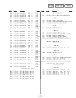
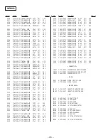
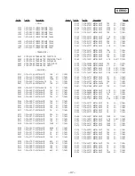
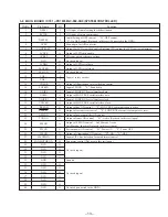
IC PIN FUNCTION DESCRIPTION
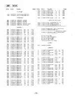
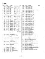
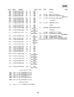
3-1. SERVO BOARD IC501 CXP84340-049Q (MD MECHANISM CONTROLLER)
Pin No.
Pin Name
I/O
Function
1
TIN3
I/O
2
TIN4
I/O
Input of 4
×
8 matrix test keys
3
TIN5
I/O
(“L” is always output, except in TEST mode)
4
TIN6
I/O
(Not used in this set) (open)
5
TIN7
I/O
6
LOAD
O
Output of control for loading motor (M903) (Cartridge loading direction)
7
EJECT
O
Output of control for loading motor (M903) (Cartridge eject direction)
8
NCO
O
Not used (open)
9
NCO
O
10
MDMON
O
Mechanical deck power ON
11
E SW
I
Input of loading end switch (S902)
“L”: Switch make
12
AGING
O
Output of aging status in TEST mode
“H”: Aging completed
“L”: Under aging
(Not used in this set)
13
AGCHK
O
Output of status when aging completed in TEST mode
“H”: Aging OK
“L”: Aging NG (Not used in this set)
14
TFTON
O
Output of free run status in TEST mode
“H”: Free run
“L” : Normal (Not used in this set)
15
NCO
O
16
NCO
O
Not used (open)
17
NCO
O
18
DFCTSEL
I
Select whether DEFECT2 function is used for CXD2650R (IC301)
“H”: Not used
“L”: Used
19
DPLLSEL
I
Select whether DPLL function is used for CXD2650R (IC301)
“H”: Not used
“L”: Used
20
EMPHSEL
I
Select whether Emphasis signal is output from pin or UNILINK
“H”: Output from pin
“L”: Output from both pin and UNILINK
21
LOCK
O
Output of CLV LOCK status in TEST mode
“H”: LOCK
“L”: UNLOCK
22
NCO
O
Not used (open)
23
2M/4M
I
Select DRAM 2M or 4M
“H”: 2M (internal DRAM)
“L”: 4M (external DRAM)
24
TAEG E
O
Output of mechanism aging completion in TEST mode (Not used in this set) (open)
25
NCO
O
Not used (open)
26
MNT0
I
Input of CXD2650R (IC301) monitor 0
27
MNT1
I
Input of CXD2650R (IC301) monitor 1
28
MNT2
I
Input of CXD2650R (IC301) monitor 2
29
MNT3
I
Input of CXD2650R (IC301) monitor 3
30
RESET
I
Input of RESET signal
31
EXTAL
I
Input of SYSTEM CLOCK (10 MHz)
32
XTAL
O
Output of SYSTEM CLOCK (10 MHz)
33
VSS
–
Ground
34
TX
O
Output of CLOCK signal (32 kHz) for clock (Not used in this set) (open)
35
TEX
I
Input of CLOCK signal (32 kHz) for clock (Not used in this set) (Connected to the GND)
36
AVSS
–
Ground pin for A/D conversion input
37
AVREF
–
Input pin for A/D conversion input reference voltage
38
INIT
I
Initial input at the reset
Pin No.
Pin Name
I/O
Function
39
TEMP
I
A/D input for temperature detection
40
ACNT
I
A/D input to select the number of Load/Eject aging times
0H - 54H (30 times), 55H - OA9H (20 times), OAAH - OFFH (10 times)
41
DO SEL
I
A/D input to select digital output bits
42
EE CS
O
Output of EEPROM selection (Not used in this set) (open)
43
EE CKO
O
Serial clock output for EEPROM (Not used in this set) (open)
44
EE SIO
I/O
EEPROM data input/output (Not used in this set) (open)
45
MD SO
O
Data output to MD servo IC (SWDT of CXD2650R in this set)
46
LINKOFF
O
“LINKOFF” pin of SONY Bus
“H”: LINKOFF
“L”: LINK connected
47
UNIREQ
O
“REQUEST” pin of SONY Bus
“H”: REQUEST ON (Not used in this set) (open)
48
UNICKI
I
“CLOCK IN” pin of SONY Bus
49
UNISI
I
“DATA IN” pin of SONY Bus
50
UNISO
O
“DATA OUT” pin of SONY Bus
51
MD CKO
O
“CLOCK OUT” pin to MD servo IC (CXD2650R in this set)
52
MD SI
I
“DATA IN” pin from MD servo IC (SRDT of CXD2650R in this set)
53
NCO
O
Not used (open)
54
SENS
I
“SENSE” input from MD servo IC (CXD2650R in this set)
55
CC XINT
I
Input of “XINT” interrupt signal from MD servo IC (CXD2650R in this set)
56
LIMIT IN
I
Input of sled most inside track detection switch
57
EJT KEY
I
Input of EJECT key
“L”: EJECT button ON
58
ERROR PWM
O
Output of C1 ATER (Not used in this set) (open)
59
MD RST
O
Output of RESET to MD servo IC (XRST of CXD2650R in this set)
/RF AMP IC (XRST of CXA2523R in this set)
60
BU IN
I
System power interruption check port
61
BUS ON
I
“BUS ON” input pin of SONY Bus
62
SQSY
I
Input of “SUBQ Sync” from MD servo IC (CXD2650R in this set)
63
C SW
I
Input of cartridge loading switch (S901)
“H”: Cartridge eject completed
“L”: Cartridge loading
64
MD LAT
O
Output of LATCH command to MD servo IC (XLAT of CXD2650R in this set)
65
MD ON
O
Power supply control to MD servo IC (CXD2650R in this set)
“H”: Power on
66
DEEMP
O
Deemphasis control
“H”: Deemphasis circuit ON
67
A MUTE
O
Output of audio mute
“H”: Mute ON
68
NCO
O
Not used (open)
69
TSTCKO
O
Output of clock for TEST mode display (Not used in this set) (open)
70
TSTSO
O
Output of data for TEST mode display (Not used in this set) (open)
71
TSTMOD
I
Input of TEST mode
“H”: Normal
“L”: TEST mode
72
VDD
–
Power supply
73
NC
–
NC pin (Connected to VDD)
74
TOUT0
O
75
TOUT1
O
Output of 4
×
8 matrix test keys (Not used in this set) (open)
76
TOUT2
O
77
TOUT3
O
78
TIN0
I/O
Input of 4
×
8 matrix test keys
79
TIN1
I/O
(“L” is always output, except in TEST mode) (Not used in this set) (open)
80
TIN2
I/O
– 11 –
– 12 –
Summary of Contents for MDX-C670
Page 3: ... 3 SECTION 2 GENERAL This section is extracted from MDX C670 instruction manual ...
Page 4: ... 4 ...
Page 5: ... 5 ...
Page 6: ... 6 ...
Page 15: ......
Page 16: ......
Page 17: ......
Page 18: ......
Page 19: ......
Page 48: ......
Page 49: ......
Page 50: ......
Page 51: ......
Page 52: ......
Page 53: ......
Page 54: ......
Page 55: ......
Page 56: ......
Page 57: ......
Page 58: ......
Page 59: ......


